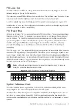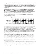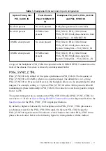
Table 1. Backplane External Clock Input Configuration
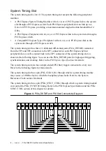
System Timing Slot
PXI_CLK10_IN
Front Chassis
Panel 10 MHz REF
IN
Backplane PXI_CLK10, PXIe_CLK100
and PXIe_SYNC100
No clock present
No clock present
Backplane generates its own clocks
No clock present
10 MHz clock
present
PXI_CLK10, PXIe_CLK100 and
PXIe_SYNC100 all phase-locked to front
Chassis Panel—10 MHz REF IN
10 MHz clock present
No clock present
PXI_CLK10, PXIe_CLK100 and
PXIe_SYNC100 all phase-locked to
System Timing Slot— PXI_CLK10_IN
10 MHz clock present
10 MHz clock
present
PXI_CLK10, PXIe_CLK100 and
PXIe_SYNC100 all phase-locked to
System Timing Slot— PXI_CLK10__IN
A copy of the backplane’s PXI_CLK10 is exported to the 10 MHz REF OUT connector on the
front of the chassis. This clock is driven by an independent buffer.
PXIe_SYNC_CTRL
PXIe_SYNC100 is by default a 10 ns pulse synchronous to PXI_CLK10. The frequency of
PXIe_SYNC100 is 10/
n
MHz, where
n
is a positive integer. The default for
n
is 1, giving
PXIe_SYNC100 a 100 ns period. However, the backplane allows
n
to be programmed to other
integers. For example, setting
n
= 3 gives a PXIe_SYNC100 with a 300 ns period while still
maintaining its phase relationship to PXI_CLK10. The value for
n
can be any positive integer
from 1 to 255.
The system timing slot has a control pin for PXIe_SYNC100 called PXIe_SYNC_CTRL for
use when
n
> 1. Refer to
System Timing Slot XP3 Connector Pinout
for the PXIe_SYNC_CTRL input specifications.
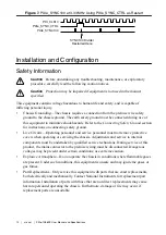
By default, a high-level detected by the backplane on the PXIe_SYNC_CTRL pin causes a
synchronous restart for the PXIe_SYNC100 signal. On the next PXI_CLK10 edge the
PXIe_SYNC100 signal restarts. This allows several chassis to have their PXIe_SYNC100 in
phase with each other. Refer to the following figure for timing details with this method.
PXIe-1086DC User Manual and Specifications
|
© National Instruments
|
11


