background image

©

 National Instruments

35 NI sbRIO-960x/962x/963x OEM Instructions & Specifications

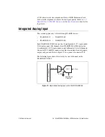
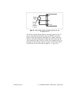
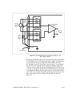
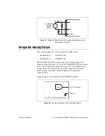
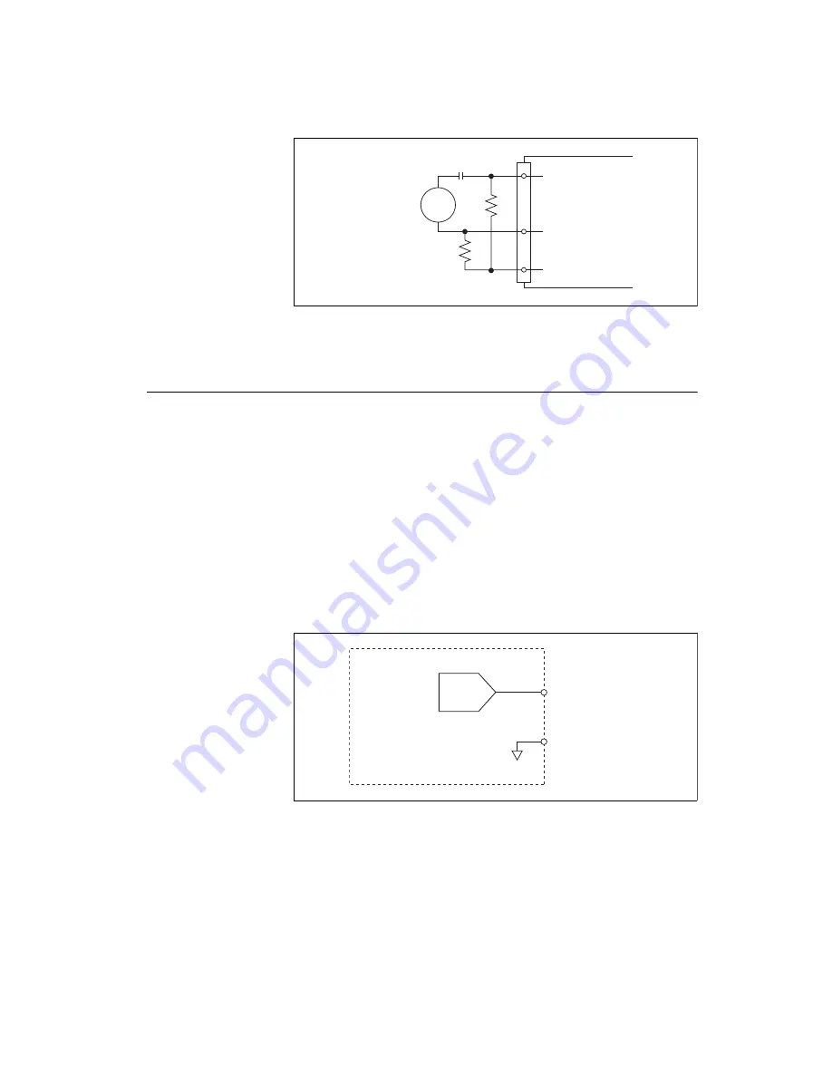
Figure 27.  

Differential Connections for AC Coupled Floating Sources with 

Balanced Bias Resistors

Integrated Analog Output

This section applies only to the following NI sbRIO devices:

The NI sbRIO-9623/9633 each have four 12-bit analog output (AO) 
channels capable of driving 0 V to 5 V. The NI sbRIO-9626-9636 each have 
four 16-bit AO channels capable of driving ±10 V. All AO channels are 
ground-referenced. Connector J503 provides connections for analog 
inputs, outputs, and grounds. Refer to Figure 17 for a pinout of 
connector J503.

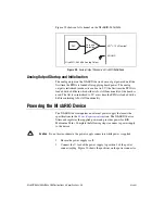
Figure 28 shows an AO channel on the NI sbRIO-9623/9633.

Figure 28.  

Analog Output Channel on NI sbRIO-9623/9633

NI sbRIO-9623

NI sbRIO-9633

NI sbRIO-9626

NI sbRIO-9636

+

AI GND

V

s

AC Co

u

pled

Flo

a

ting

S

ign

a

l

S

o

u

rce

AI+

AI–

AC Co

u

pling

DAC

NI 

sb

RIO - 962

3

/

33

 An

a

log O

u

tp

u

t

AO 0-5 V Nomin

a

AO GND

Summary of Contents for sbRIO-9605

Page 1: ...e section shows which models support the feature Figure 1 NI sbRIO 9636 Caution The NI sbRIO device must be installed inside a suitable enclosure prior to use Hazardous voltages may be present Caution National Instruments makes no product safety electromagnetic compatibility EMC or CE marking compliance claims for NI sbRIO devices The end product supplier is responsible for conformity to any and a...

Page 2: ... Get Started This section lists the software and hardware you need to start programming the NI sbRIO device Software Requirements You need a development computer with the following software installed on it Go to ni com info and enter the Info Code rdsoftwareversion for information about software version compatibility LabVIEW 2011 1 or later LabVIEW Real Time Module 2011 1 or later LabVIEW FPGA Mod...

Page 3: ...gure 2 All possible components on the NI sbRIO Device 1 W502 RS 485 COM3 2 W503 RS 232 COM2 3 J504 SDHC 4 J506 Power Connector 5 Chassis Ground Bracket 6 J507 USB Host Port 7 W500 CAN CAN0 8 J505 RJ 45 Ethernet Port 9 W501 RS 232 Serial COM1 10 Reset Switch 11 LEDs 12 J502 DIO 13 J503 MIO 14 Mounting Holes Connected to Chassis Ground 15 FPGA 16 NAND Flash 17 Processor 18 DDR Memory 19 J1 RIO Mezza...

Page 4: ... 1 sbRIO 9623 256 MB 128 MB 2 1 LX25 4 16ch 12bit 4ch 12bit 1 sbRIO 9626 512 MB 256 MB 2 1 1 1 1 LX45 4 16ch 16bit 4ch 16bit 1 sbRIO 9633 256 MB 128 MB 2 1 1 1 1 LX25 28 16ch 12bit 4ch 12bit sbRIO 9636 512 MB 256 MB 2 1 1 1 1 LX45 28 16ch 16bit 4ch 16bit Table 2 NI sbRIO Connector Descriptions Connector Description Manufacturer Part Number Recommended Mating Connector NI Solution Power 2 position ...

Page 5: ...s be 0 15 mm taller than the combined height of the RMC and mating connectors Therefore to determine the required standoff height you must add the heights of the connectors plus 0 15 mm For example if you are using a SEAM 40 03 0 S 06 2 connector to mate to the RMC connector SEAF 40 06 5 S 06 2 the required standoff height is 3 0 mm 6 5 mm 0 15 mm 9 65 mm Standoffs of this height are available fro...

Page 6: ...oduct page at ni com Figure 3 shows the dimensions of the primary side of the NI sbRIO device Figure 3 NI sbRIO 9605 9606 Primary Side Dimensions in mm in 1 Back of Front Panel 0 000 0 64 025 0 000 FPGA NAND Flash Processor 20 63 812 Pin 1 17 17 676 18 13 714 Pin 2 49 97 1 967 69 96 2 754 74 24 2 923 30 81 1 213 52 91 2 083 61 82 2 434 69 47 2 735 Pin 1 Pin 2 77 59 3 055 7 31 288 59 18 2 330 DDR M...

Page 7: ...ry side of the NI sbRIO device Figure 4 NI sbRIO 9605 9606 Secondary Side Dimensions in mm in 1 Holes and Keepouts Sized for M3 Standoff 4 5 mm Hex or 4 40 Standoff 3 16 in Hex 4x Ø 3 18 125 0 000 26 67 1 050 3 2 126 Pin 1 96 74 3 809 98 4 3 874 40 03 1 576 76 84 3 025 1 73 63 2 899 96 52 3 800 0 000 71 72 2 824 102 87 4 050 ...

Page 8: ... in mm in 1 Back of Front Panel 0 0 000 139 07 5 475 149 86 5 900 0 0 000 Pin 1 17 17 0 676 18 13 0 714 Pin 2 NAND Flash 49 96 1 967 59 18 2 330 DDR Memory 69 95 2 754 74 24 2 923 77 60 3 055 Processor 84 51 3 327 17 12 0 674 0 64 0 025 Pin 1 Pin 2 Pin 2 Pin 1 Pin 1 Pin 2 142 43 5 607 61 82 2 434 FPGA 52 91 2 083 30 81 1 213 7 32 0 288 20 63 0 812 69 47 2 735 Pin 2 Pin 1 150 73 5 934 Pin 1 Pin 2 1...

Page 9: ...de of the NI sbRIO device Figure 6 NI sbRIO 9623 9633 9626 9636 Secondary Side Dimensions in mm in 1 Holes and Keepouts Sized for M3 Standoff 4 5 mm Hex or 4 40 Standoff 3 16 in Hex 3 20 0 126 40 03 1 576 76 84 3 025 150 47 5 924 Pin 1 0 0 000 26 67 1 050 3 18 0 125 6x Ø 96 75 3 809 98 40 3 874 102 87 4 050 0 0 000 153 67 6 050 1 ...

Page 10: ...ng Power Connector 2 Minimum Keepaway for RIO Mezzanine Card Components 3 4 40 threads Maximum Torque of 0 41 N m 3 6 lb in 0 000 Ø 3 118 18 16 715 16 630 6 16 242 0 000 2 16 085 5 34 210 2 54 100 5 08 200 7 62 300 10 16 400 33 8 1 331 49 93 1 966 57 51 2 264 70 01 2 756 89 81 3 536 95 21 3 748 8 76 345 3 66 144 6 32 249 6 15 242 19 48 767 76 84 3 025 4x Ø 2 8 071 1 2 3 18 16 0 715 6 15 0 242 2 56...

Page 11: ...tors The secondary side is the bottom Figures 9 to 12 show the maximum component heights for the different regions of the primary and secondary sides Note In addition to the maximum component heights you must also observe minimum keepaway distances for adjacent PCBs and surfaces Allow 19 05 mm 0 75 in from the surface of the primary side and 7 62 mm 0 300 in from the surface of the secondary side ...

Page 12: ...ions Specifications 12 ni com Figure 10 NI sbRIO 9623 9633 9626 9636 Maximum Component Height of Primary Side in mm in Max Component Height 4 06 0 160 Max Component Height 9 53 0 375 Max Component Height 17 27 0 680 31 75 1 250 96 52 3 8 ...

Page 13: ... 13 NI sbRIO 960x 962x 963x OEM Instructions Specifications Figure11 NIsbRIO 9605 9606MaxComponentHeightofSecondarySideinmm in Max Component Height 6 15 0 242 Max Component Height 7 62 0 300 60 96 2 400 11 43 450 10 16 400 ...

Page 14: ... OEM Instructions Specifications 14 ni com Figure 12 NI sbRIO 9623 9633 9626 9636 Max Component Height of Secondary Side in mm in Max Component Height 6 15 0 242 Max Component Height 7 62 0 300 60 96 2 400 11 43 450 10 16 400 ...

Page 15: ...unting Procedure Note Mounting holes on the NI sbRIO device are designed to accommodate M3 or 4 40 fasteners and standoffs or bosses up to 4 5 mm or 3 16 in in diameter Caution Maintain a minimum keepaway distance of 7 62 mm 0 300 in when mounting NI sbRIO devices with an RMC connector and a minimum keepaway distance of 6 15 mm 0 242 in when mounting NI sbRIO devices without an RMC connector 1 M3 ...

Page 16: ...zanine Card This section applies only to the following NI sbRIO devices Figure 14 NI sbRIO Device Mating Procedure NI sbRIO 9605 NI sbRIO 9623 NI sbRIO 9606 NI sbRIO 9626 1 M3 or 4 40 Standoff Not Included 2 RIO Mezzanine Card RMC Connector 3 Example RMC Not Included 4 Mounting Surface Not Included 1 2 3 4 ...

Page 17: ...n connecting the NI sbRIO device to external devices ensure that stray ground currents are not using the device as a return path Significant stray currents traversing through the NI sbRIO device can result in device failure To verify correct grounding of the NI sbRIO device make sure the current flowing into the power connector equals the current flowing out of the power connector These currents s...

Page 18: ...C SHIELD NC SHIELD CAN0_H V GND NC 10 9 8 7 6 5 4 3 2 1 Pin 1 RXD DTR DSR CTS SHIELD DCD GND RTS TXD RI 10 9 8 7 5 6 4 3 2 1 Pin 1 NC RXD NC TXD SHIELD GND RXD NC NC TXD 10 9 8 7 6 5 4 3 2 1 RXD DTR DSR CTS SHIELD DCD GND RTS TXD RI 10 9 8 7 5 6 4 3 2 1 W500 CAN 0 W501 RS 232 COM1 W502 RS 485 COM3 W503 RS 232 COM2 Pin 1 Pin 1 J503 J502 W502 W503 W500 W501 ...

Page 19: ... D GND D GND D GND D GND D GND D GND 5V DIO26 DIO25 DIO23 DIO22 DIO21 DIO20 DIO27 DIO24 DIO19 DIO18 DIO17 DIO16 DIO15 DIO14 DIO13 DIO12 DIO11 DIO10 DIO9 DIO8 DIO7 DIO6 DIO5 DIO4 1 2 3 4 5 6 7 8 9 10 11 12 13 14 15 16 17 18 19 20 21 22 23 24 25 26 27 28 29 30 31 32 33 34 35 36 37 38 39 40 41 42 43 44 45 46 47 48 49 50 DIO3 DIO1 DIO0 NC NC NC AO3 DIO2 NC AO2 AO1 AO0 AI GND AI7 AI GND AI6 AI5 AI GND ...

Page 20: ...processor functionality such as serial CAN USB or Ethernet should contact a local National Instruments representative for custom design opportunities A non recurring engineering charge NRE may apply Note Reserved and unused lines should be left disconnected on RIO Mezzanine Cards Future versions of this manual may update their definition Note National Instruments suggests using pins DIO0 through D...

Page 21: ...nstruments 21 NI sbRIO 960x 962x 963x OEM Instructions Specifications Figure 18 RMC Connector Location and Dimensions on Example RIO Mezzanine Card 98 40 3 000 96 75 3 809 3 20 0 126 40 03 1 576 Pin 1 0 000 0 000 ...

Page 22: ... 97 DIO95 98 GND 99 DIO31 100 DIO78 101 GND 102 DIO14 103 GND 104 DIO62 105 DIO30 106 GND 107 DIO45 108 DIO13 109 DIO94 110 DIO61 111 GND 112 DIO77 113 DIO44 114 GND 115 DIO93 116 GND 117 DIO29 118 DIO76 119 GND 120 DIO12 121 GND 122 DIO60 123 DIO28 124 GND 125 DIO43 126 DIO11 127 DIO92 128 DIO59 129 GND 130 DIO75 131 DIO42 132 GND 133 DIO91 134 GND 135 DIO27 136 DIO74 137 GND 138 DIO10 139 GND 14...

Page 23: ...ime will be reset during a power cycle Batteries connected to VBAT must have a nominal output between 3 0 V and 3 6 V and a maximum output of 3 7 V If VBAT is not being used leave it disconnected USB on RMC Connector The USB pair on the RMC Connector has a 90 Ω differential trace impedance To ensure the best possible signal integrity route the USB pair with a similar trace impedance If USB is not ...

Page 24: ...O lines are floating before and during FPGA configuration To ensure startup values place pull up or pull down resistors on a RIO Mezzanine Card The DIO channels on the NI sbRIO device are routed with a 55 Ω characteristic trace impedance Route all RIO Mezzanine Cards with a similar impedance to ensure the best signal quality Refer to 3 3 V Digital I O on RIO Mezzanine Card Connector in the Specifi...

Page 25: ...9623 9633 devices has 16 multiplexed 0 5 V single ended 12 bit analog input AI channels Each NI sbRIO 9626 9636 device has 16 multiplexed 10 V single ended or eight differential 16 bit AI channels Connector J503 the MIO connector provides connections for analog inputs outputs and grounds Refer to Figure 17 for a pinout of connector J503 The following figure shows the circuitry for one AI channel o...

Page 26: ...there are 216 65 536 possible values These values are spread evenly across the input range and the voltage difference between values is proportional to the input range selected for the channel The voltage difference between values is the size of the least significant bit LSB size for the channel The following equation shows how to calculate the LSB size for a channel set to the 10 V to 10 V input ...

Page 27: ...tant for all range selections The signal voltage Vs which is equivalent to subtracting AI from AI must be less than or equal to the range selection of the given channel If Vs is greater than the range selected the signal clips and information is lost The total working voltage of the positive input which is equivalent to Vcm Vs or subtracting AIGND from AI must be less than the maximum working volt...

Page 28: ... impedance sources increase settling errors and decrease accuracy at fast scanning rates You can reduce impedance by connecting a voltage follower circuit between the signal source and the AI pin of the channel For more information about reducing impedance go to ni com info and entering the Info Code rdbbis 2 Use Short High Quality Cabling Using short high quality cables can minimize several effec...

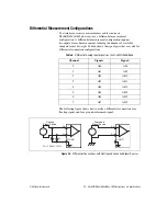
Page 29: ... from 16 to eight Table 6 shows the signal pairs that are valid for differential connection configurations The following figure shows how to make a differential connection for a floating signal and for a ground referenced signal Figure 23 Differential Connections with Floating and Grounded Signal Sources Table 6 Differential Analog Input Signals on the NI sbRIO 9626 9636 Channel Signal Signal 0 AI...

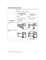
Page 30: ... Floating Signal Sources Not Connected to Building Ground Ground Referenced Signal Sources Examples Ungrounded thermocouples Signal conditioning with isolated outputs Battery devices Example Plug in instruments with non isolated outputs Differential Referenced Single Ended RSE AI AI AI GND Signal Source AI AI AI GND Signal Source AI AI GND Signal Source Ground loop potential VA VB are added to mea...

Page 31: ...l through noisy environments Two analog input channels AI and AI are available for the signal DIFF signal connections reduce noise pickup and increase common mode noise rejection DIFF signal connections also allow input signals to float within the common mode limits of the PGIA Refer to the Using Differential Connections for Floating Signal Sources section for more information about differential c...

Page 32: ...signal to AI GND as well as to AI without using resistors This connection works well for DC coupled sources with low source impedance less than 100 Ω Figure 24 Differential Connections for Floating Signal Sources without Bias Resistors However for larger source impedances this connection leaves the DIFF signal path significantly off balance Noise that couples electrostatically onto the positive li...

Page 33: ...ositive input and AI GND as shown in Figure 26 This fully balanced configuration offers slightly better noise rejection but has the disadvantage of loading the source down with the series combination sum of the two resistors If for example the source impedance is 2 kΩ and each of the two resistors is 100 kΩ the resistors load down the source with 200 kΩ and produce a 1 gain error R is about 100 ti...

Page 34: ...ignificantly load the source but small enough not to produce significant input offset voltage as a result of input bias current typically 100 kΩ to 1 MΩ In this case connect the negative input directly to AI GND If the source has high output impedance balance the signal path as previously described using the same value resistor on both the positive and negative inputs be aware that there is some g...

Page 35: ...riving 0 V to 5 V The NI sbRIO 9626 9636 each have four 16 bit AO channels capable of driving 10 V All AO channels are ground referenced Connector J503 provides connections for analog inputs outputs and grounds Refer to Figure 17 for a pinout of connector J503 Figure 28 shows an AO channel on the NI sbRIO 9623 9633 Figure 28 Analog Output Channel on NI sbRIO 9623 9633 NI sbRIO 9623 NI sbRIO 9633 N...

Page 36: ...zed to 0 V every time the FPGA is loaded with a bitfile containing AI or AO functionality Powering the NI sbRIO Device The NI sbRIO device requires an external power supply that meets the specifications in the Power Requirements section The NI sbRIO device filters and regulates the supplied power and provides power for RIO Mezzanine Cards Complete the following steps to connect a power supply to t...

Page 37: ...to the device During the POST the Power and Status LEDs turn on When the Status LED turns off the POST is complete If the LEDs do not behave in this way when the system powers on refer to the Understanding LED Indications section Device Startup Options You can configure the following device startup options in NI Measurement Automation Explorer MAX Safe Mode Console Out IP Reset No App No FPGA App ...

Page 38: ...ject Explorer window in LabVIEW 2 Select Properties 3 In the General category of the FPGA Target Properties dialog box place a check in the Run when loaded to FPGA checkbox 4 Compile the FPGA VI Connecting the NI sbRIO Device to a Network Connect the device to an Ethernet network using the RJ 45 Ethernet port on the controller front panel Use a standard Category 5 CAT 5 or better shielded twisted ...

Page 39: ...ons to a CAN bus CAN enabled NI sbRIO devices have pins for CAN_H and CAN_L which can connect to the CAN bus signals The CAN port uses an NXP PCA82C251T high speed CAN transceiver that is fully compatible with the ISO 11898 standard and supports baud rates up to 1 Mbps The port has two common pins GND that serve as the reference ground for CAN_H and CAN_L You can connect the CAN bus reference grou...

Page 40: ...esistors The termination resistors Rt should match the nominal impedance of the CAN cable and therefore comply with the values in Table 10 Table 9 ISO 11898 Specifications for Characteristics of a CAN_H and CAN_L Pair of Wires Characteristic Value Impedance 95 Ω minimum 120 Ω nominal 140 Ω maximum Length related resistance 70 mΩ m nominal Specific line delay 5 ns m nominal Table 10 Termination Res...

Page 41: ...trical characteristics of the nodes on the network If all nodes meet the ISO 11898 requirements you can connect at least 30 nodes to the bus You can connect higher numbers of nodes if the electrical characteristics of the node do not degrade signal quality below ISO 11898 signal level specifications USB Port This section applies only to the following NI sbRIO devices The NI sbRIO devices populated...

Page 42: ...m info and enter the Info Code criosntp Using the Reset Button Pressing the Reset button reboots the processor The FPGA continues to run unless you select the Autoload VI on device reboot boot option Refer to the Device Reset Options section for more information Note To force the device into safe mode hold the reset button down for 5 seconds then release The device will be in safe mode with output...

Page 43: ...device is adequate Status LED The STATUS LED is off during normal operation The NI sbRIO device runs a power on self test POST when you apply power to the device During the POST the Power and Status LEDs turn on When the Status LED turns off the POST is complete The NI sbRIO Device indicates specific error conditions by flashing the Status LED a certain number of times every few seconds as shown i...

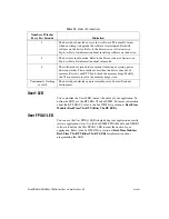
Page 44: ...s for information about programming this LED Table 12 Status LED Indications Number of Flashes Every Few Seconds Indication 2 The device has detected an error in its software This usually occurs when an attempt to upgrade the software is interrupted Reinstall software on the device Refer to the Measurement Automation Explorer Help for information about installing software on the device 3 The devic...

Page 45: ...me behavior The NI sbRIO device attempts to establish a new DHCP connection If it fails it assigns itself a link local IP address If the DHCP connection is successful and appropriate for your application skip to step 4 3 Configure the IP and other network settings in MAX 4 Press and release the Reset button to reboot the device Note If the device is restored to the factory network settings the Lab...

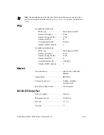
Page 46: ...2 Number of DSP48s 38 Available block RAM 936 kbits Number of DMA channels 5 NI sbRIO 9606 9626 9636 FPGA type Xilinx Spartan 6 LX45 Number of flip flops 54 576 Number of 6 input LUTs 27 288 Number of DSP48s 58 Available block RAM 2 088 kbits Number of DMA channels 5 Network Network interface 10BaseT and 100BaseTX Ethernet Compatibility IEEE 802 3 Communication rates 10 Mbps 100 Mbps auto negotiat...

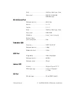
Page 47: ...y Odd Even Mark Space None Flow control XON XOFF Wire Mode 4 wire 2 wire 2 wire auto Isolation Voltage port to earth ground None Embedded CAN Transceiver NXP PCA82C251T Maximum baud rate 1 Mbps Minimum baud rate 10 kbps USB Port Compatibility USB 2 0 High Speed Maximum data rate 480 Mb s Maximum current 500 mA Internal RTC Accuracy 200 ppm 35 ppm 25 C VBAT input range 3 0 to 3 6 V Nominal 3 7 V Ma...

Page 48: ...nfo and enter the Info Code RMCDIO Input logic levels Input low voltage VIL 0 V min 0 8 V max Input high voltage VIH 2 0 V min 3 465 V max Output logic levels Output high voltage VOH sourcing 3 mA 2 4 V min 3 465 V max Output low voltage VOL sinking 3 mA 0 0 V min 0 4 V max 3 3 V Digital I O on 50 Pin IDC Connector Number of DIO channels NI sbRIO 9623 9626 4 NI sbRIO 9633 9636 28 Max tested curren...

Page 49: ... overload 1 kΩ Overvoltage protection None AI accuracy Note For information about measuring the local ambient temperature refer to the Environmental section INL 0 024 of range DNL 0 024 of range Input bandwidth 3 dB 6 MHz NI sbRIO 9626 9636 Number of channels 16 single ended or 8 differential ADC Resolution 16 bits Maximum aggregate sampling rate 200 kS s Input range 10 V 5 V 2 V 1 V Measurement C...

Page 50: ...drift 12 ppm of reading C Offset drift 4 ppm of range C AI Noise INL 64 ppm of range max DNL No missing codes guaranteed Range Working voltage 10 V 11 V 5 V 10 5 V 2 V 9 V 1 V 8 5 V Measurement Conditions Range Percent of Reading Gain Error Percent of Range Offset Error Typical 25 C 5 C 1 V 0 042 0 007 2 V 0 007 5 V 0 007 10 V 0 008 Max 40 to 85 C 1 V 0 380 0 179 2 V 0 360 0 138 5 V 0 348 0 113 10...

Page 51: ...600 kHz typical Settling error multichannel scanning 60 ppm step size typical Crosstalk 10 kHz 70 dB Typical performance graphs CMRR dB Frequency Hz 10 100 1000 10000 110 100 105 90 95 85 80 70 75 1 V Range 2 V Range 5 V Range 10 V Range Normalized Signal Amplitude dB Frequency Hz 1000 10000 100000 1000000 1 2 4 7 8 6 5 3 1 0 ...

Page 52: ...ing one AO channel in a loop with the FPGA top level clock set to 40 MHz 2 When power is applied the analog outputs remain high impedance until the FPGA loads for the first time When the FPGA loads the analog outputs become low impedance sources driving 0 V During the transition from high to low impedance the outputs typically glitch for about 60 µs The magnitude of the glitch is inversely proport...

Page 53: ...6 kS s Range 10 V Overrange operating voltage Minimum 10 3 V Typical 10 6 V Max 10 9 V Output impedance 0 4 Ω typical Current drive 3 mA channel max Protection Short circuit to ground Power on state2 0 V Measurement Conditions Percent of Reading Gain Error Percent of Range Offset Error Typical 25 C 5 C 0 12 0 02 Max 40 to 85 C 0 80 0 12 Range is 5 V 1 This is the maximum update rate when running o...

Page 54: ...connected to the power connector Refer to Figure 2 for the location of the power connector Refer to the Powering the NI sbRIO Device section for information about connecting the power supply Caution Exceeding the power limits may cause unpredictable behavior by the device Recommended power supply 55 W 30 VDC max Power supply voltage range 9 30 VDC1 Measurement Conditions Percent of Reading Gain Er...

Page 55: ...output across the RMC Connector PUSB is the power consumption of a device plugged into the USB port PSD is the power consumption of an SD card plugged into the SD slot PAO is the power consumption of the Analog output across the MIO connector When calculating each component of the maximum power consumption the following efficiency factors must be used η3 3 V ηDIO and ηSD 80 η5 V and ηUSB 90 ηAO 50...

Page 56: ...requirement 17 11 W Note These calculations are intended to approximate the maximum power requirements for an NI sbRIO device system For a more accurate estimate of a specific application s power consumption it is recommended to directly measure a board running the application in an environment representative of the intended use case 1 The SD specification allows 200 mA maximum current draw for an...

Page 57: ...onmental The NI sbRIO device is intended for indoor use only Local ambient temperature near device IEC 60068 2 1 IEC 60068 2 2 NI sbRIO 960x 40 to 85 C NI sbRIO 962x 40 to 85 C NI sbRIO 963x 40 to 85 C Note Measure the local ambient temperature by placing thermocouples on both sides of the PCB 0 2 in 5 mm from the board surface Avoid placing thermocouples next to hot components such as the FPGA pr...

Page 58: ...so to ni com info and enter the Info Code sbriocooling Storage temperature IEC 60068 2 1 IEC 60068 2 2 40 to 85 C Operating humidity IEC 60068 2 56 10 to 90 RH noncondensing Storage humidity IEC 60068 2 56 5 to 95 RH noncondensing Maximum altitude 5 000 m Pollution Degree IEC 60664 2 Physical Characteristics Weight NI sbRIO 9605 85 g 2 998 oz NI sbRIO 9606 89 g 3 139 oz NI sbRIO 9623 123 g 4 24 oz...

Page 59: ...signing and manufacturing products in an environmentally responsible manner NI recognizes that eliminating certain hazardous substances from our products is beneficial to the environment and to NI customers For additional environmental information refer to the NI and the Environment Web page at ni com environment This page contains the environmental regulations and directives with which NI complie...

Page 60: ...er import export data 2012 National Instruments All rights reserved 373378C 01 Aug 12 Where to Go for Support The National Instruments Web site is your complete resource for technical support At ni com support you have access to everything from troubleshooting and application development self help resources to email and phone assistance from NI Application Engineers National Instruments corporate ...

Reviews: