background image


http://www.national.com 

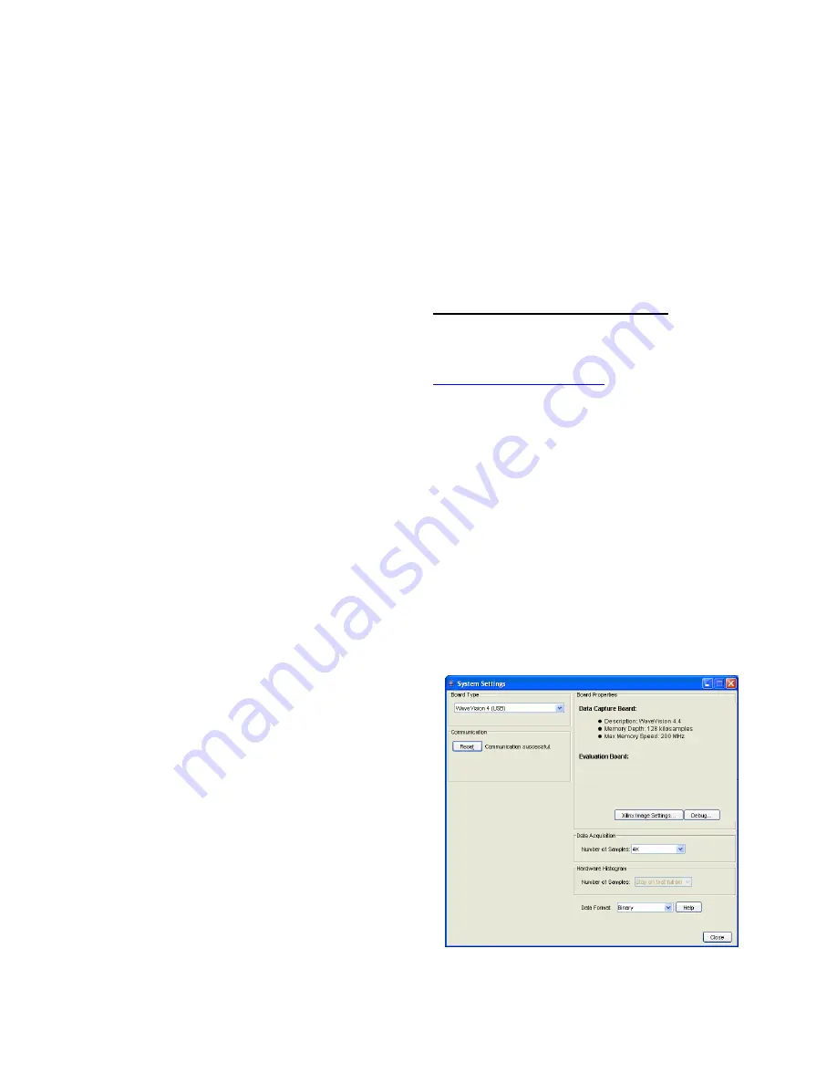
Figure 9: System Settings window 

4.6 Automatic Conversion Mode 

The Automatic Conversion Mode configures the 
ADC to continually perform conversions without 
receiving “read” instructions from the I

2

controller.  It is activated by writing a non-zero 
value into the Cycle Time bits “D[7:5]” of the 
Configuration Register. Various automatic 
conversion rates are supported. 

Refer to 

Section 1.9

 of the Datasheet for a 

detailed description of the Automatic Conversion 
Mode. 

4.7 Power Supply Connections 

The analog supply voltage (V

A

) can range from 

+2.7V to +5.5V. The Evaluation system provides a 
handful of power supply options via the JP5 
header (

see Table 1

).  V

A

 can be driven by the 

LM4050-4.1 Shunt Reference, the LM1117MPX-
3.3 LDO from the WV4 board, or an external 
supply. National recommends the LM4050 
precision reference for the ADC121C021. 

NOTE: In Computer mode, if V

A

 is driven with less 

than 3.3V in Computer mode, an external 3.3V 
pull-up supply is needed.  This will ensure the 
3.3V CMOS logic thresholds of the WaveVision4 
board are met for SDA and SCL.  

To use an external pull-up supply, remove the 
jumper at JP2 and connect the supply to pin 2 of 
JP2 or VIA6.   An external pull-up supply will also 
improve the dynamic performance of the ADC. 

Typical supply currents when applying an external 
supply to TP7 (VA_EXT) and performing ADC 
conversions are as follows: 


For V

A

 = +3.3V,  I = 8mA  


For V

A

 = +5.0V,  I = 11mA


Note:  A majority of this current is for powering 
devices external to the ADC121C021 such as the 
pull-up resistors and the input amplifier.   

When operating in the computer mode, the supply 
voltage for V

A

 can be applied externally or 

supplied directly by the WV4 board through J1. 
The external supply voltage is selected by placing 
a jumper across pins 9 & 10 of JP5, applying a 
power source with a 300mA current limit to TP7, 
and grounding TP6.  To use the 5.0V supply 
directly from the WV4 board, place a shorting 
jumper across pins 3 & 4 of JP5. To use the 3.3V 
supply directly from the WV4 board, place a 
shorting jumper across pins 1 & 2 of JP5.  To use 
the LM4050 4.1V Shunt Reference, place a 
shorting jumper across pins 7 & 8 of JP5.  For the 
best performance, use a clean external supply. 

When operating in Stand Alone mode, always use 
an external supply.  Apply a +5.0V power source 
with a current limit of 100mA to TP7, ground TP6, 
and place a shorting jumper across pins 9 & 10 of 
JP5. 

Note: The +3.3V required to power the EEPROM 
(U4) is obtained through J2 from the WV4 board. 
The EEPROM is used to identify the type of Eval 
Board connected to the WaveVision system in 
Computer Mode.


5.0 Software Operation and Settings 

The WaveVision 4 software is included with the 
WV4 board and the latest version can be 
downloaded for free from National's web site at 

http://www.national.com/adc

. WaveVision4 

software version 4.4 or later is required to 
evaluate this device with the WaveVision system.  

5.1 Software Quick Start 

To install this software, follow the procedure in the 
WV4 Board User's Guide.  Once the software is 
installed, run and set it up as follows: 

1.  Connect the WV4 board to the host computer 

with a USB cable. 

2.  From the WaveVision main menu, go to 

Settings and then Capture Settings to open 
the System Settings window (

Figure 9

) and 

select the following: 

 WaveVision 

(USB) 

  Number of Samples: 2k to 128k, as 

desired 

  Data Format: Binary 


Summary of Contents for ADC081C021

Page 1: ...s from www national com National Semiconductor January 3 2008 Rev 1 1 CC RoHS Compliant Evaluation Board User s Guide I2 C Compatible 12 Bit 10 Bit or 8 Bit Analog to Digital Converter ADC with Alert Function 12 bit 10 bit 8 bit ALERT Option ADC121C021 ADC101C021 ADC081C021 ADDRESS Option ADC121C027 ADC101C027 ADC081C027 ...

Page 2: ...ircuitry 7 4 4 I 2 C Interface 7 4 5 Alert Function 7 4 6 Automatic Conversion Mode 8 4 7 Power Supply Connections 8 5 0 Software Operation and Settings 8 5 1 Software Quick Start 8 5 2 Data Analysis 9 5 3 Register Control 10 5 4 Troubleshooting WaveVision 11 6 0 Evaluation Board Specifications 12 7 0 Test Points Connectors and Jumpers 12 8 0 Hardware Schematic 13 9 0 Evaluation Board Layers 14 10...

Page 3: ...the board to evaluate the ADC121C021 s performance In the Computer mode data capture and evaluation are simplified by connecting the evaluation board to National Semiconductor s WaveVision 4 Data Capture Board order number WAVEVSN BRD 4 1 or higher which connects to a personal computer through a USB port and runs WaveVision 4 software revision 4 4 or higher The latest version of the WaveVision 4 s...

Page 4: ...put signal Figure 3 Figure 2 DC Coupled Input Configuration Figure 3 AC Coupled Input Configuration If needed the input can be terminated by adding an appropriate termination resistor at R3 The V_IN footprint J2 has been stuffed with a single pin header for testing typical slow moving DC input signals An SMA footprint is also included on the PCB and should be used for precise dynamic performance e...

Page 5: ...rrent limit to power connector TP7 Ground TP6 4 Move the shorting jumper at JP5 to pins 9 10 NOTE only two consecutive pins may be shorted on JP5 at a time 5 Turn on the power supply 6 Connect the input signal to the test point at J2 The input signal return can be connected to ground at TP3 Please note the evaluation board is assembled for a DC coupled input source The board is designed for an AC ...

Page 6: ...Software Operation and Settings to setup the WaveVision 4 software 4 0 Functional Description 4 1 Jumper Settings Table 1 describes the function of the various jumpers on the ADC121C021 evaluation board The evaluation board schematic is shown in Figure 10 Jumper Pins 1 2 Pins 2 3 JP1 Select direct VIN circuit Select Amplified VIN circuit LMP7731 JP2 Enable I2 C Pull up resistors JP3 Permanently sh...

Page 7: ... be better than 90dBc THD 4 3 ADC Reference Circuitry The ADC121C021 family is internally referenced Therefore the Analog to Digital converter gets its reference from the analog supply VA Hence a clean analog supply must be used to guarantee the performance of the ADC 4 4 I 2 C Interface Please refer to section 1 7 of the ADC121C021 datasheet for a detailed description of the I 2 C interface The b...

Page 8: ...rating in the computer mode the supply voltage for VA can be applied externally or supplied directly by the WV4 board through J1 The external supply voltage is selected by placing a jumper across pins 9 10 of JP5 applying a power source with a 300mA current limit to TP7 and grounding TP6 To use the 5 0V supply directly from the WV4 board place a shorting jumper across pins 3 4 of JP5 To use the 3 ...

Page 9: ...ert function and Automatic Conversion Mode are setup through the Configuration register After making changes to a register value press the Enter key to write the register Figure 10 10 To capture a dataset from the ADC navigate back to the main WaveVision window 11 After the steps outlined in Section 3 2 are completed click on Acquire then Samples from the Main Menu you can also press the F1 shortc...

Page 10: ... the Control Panel window Each of the registers is read and displayed in the control panel To write to a register simply type in the 8 bit or 16 bit hex value to be written to the register and press Enter All hex values are assumed to be right justified Zeros are written to unspecified bits Many functions of the ADC121C021 are enabled through the internal registers Please refer to Section 1 6 on I...

Page 11: ...utions D and E 5 4 2 Solutions Solution A Ensure power is supplied to the VA supply on the board A single jumper must be placed across either pins 1 2 pins 3 4 pins 7 8 or pins 9 10 of JP5 to select the board s power source If using the Shunt Reference pins 1 2 of JP7 must be shorted The VA supply is measured by probing VIA10 Solution B Ensure the pull up resistors are powered R8 and R9 In Compute...

Page 12: ...und Located at the bottom right of the board TP9 WV_CLK_IN Not Used TP10 AGND Ground Located at the right side of the board Connectors on the ADC121C021 Evaluation Board J1 WV4S 14 pin dual row right angle male header Connects to WV4 board J2 V_IN Analog Input of the Eval Board Selection Jumpers on the ADC121C021 Evaluation Board Refer to table 1 in Section 4 0 for configuration details JP1 V_IN S...

Page 13: ... 7 9 JP5 1 1 TP7 VA_EXT L3 0 Ohm R 1 2 JP7 VA_EXT_SHUNT R12 0 1 1 VIA6 C7 10 0uF 1 2 JP2 V_PULL L1 100uH 1 2 3 JP1 INPUT SELECT 1 1 TP10 AGND 1 1 VIA5 R10 0 1 1 TP6 AGND C4 0 1uF R6 20 1 1 VIA10 R2 0 R19 51 1 2 3 JP6 CLK SELECT R18 NS 2 3 4 5 1 J2 V_IN 1 1 TP9 VA_EXT R1 NS 1 1 TP2 AGND A0 1 A1 2 A2 3 GND 4 SDA 5 SCL 6 WP 7 VCC 8 U4 24C02 C3 10 0uF 1 1 VIA11 C10 0 Ohm R 1 1 VIA1 C9 1 0uF 1 1 VIA4 1...

Page 14: ... national com 14 9 0 Evaluation Board Layers Figure 11 ADC121C021 Evaluation Board All Layers with Silk Screen Figure 12 ADC121C021 Evaluation Board Top Layer Figure 13 ADC121C021 Evaluation Board Bottom Layer ...

Page 15: ...6513 40 ND 1 JP8 NS JUMPER 1 J1 WV4S HEAD Digikey S5803 07 ND Sullins PRPN072PARN RC 1 J2 V_IN TP Center Via of SMA Digikey 5011K ND 2 L1 L2 100uH IND Digikey 490 1056 1 ND Murata BLM31PG121SN1L 1 L3 0 Ohm R 0 Ohm RES 9 R1 R3 R4 R7 R11 R13 R14 R17 R18 NS RES 4 R2 R5 R10 R12 0 RES 1 R6 20 RES 2 R8 R9 2K RES 2 R15 R19 51 RES 1 R16 500 RES 1 TP2 AGND TP NS 2 TP3 TP6 AGND TP Digikey 5011K ND 3 TP5 TP8...

Page 16: ...F THE PRESIDENT OF NATIONAL SEMICONDUCTOR CORPORATION As used herein 1 Life support devices or systems are devices or systems which a are intended for surgical implant into the body or b support or sustain life and whose failure to perform when properly used in accordance with instructions for use provided in the labeling can be reasonably expected to result in a significant injury to the user 2 A...

Page 17: ...ency energy and has not been tested for compliance with the limits of computing devices pursuant to part 15 of FCC or ICES 003 rules which are designed to provide reasonable protection against radio frequency interference Operation of the equipment may cause interference with radio communications in which case the user at his own expense will be required to take whatever measures may be required t...

Page 18: ... its gain should be so chosen that the equivalent isotropically radiated power e i r p is not more than that necessary for successful communication This radio transmitter has been approved by Industry Canada to operate with the antenna types listed in the user guide with the maximum permissible gain and required antenna impedance for each antenna type indicated Antenna types not included in this l...

Page 19: ...er you obtained the Technical Regulations Conformity Certification as provided in Radio Law of Japan with respect to this product Also please do not transfer this product unless you give the same notice above to the transferee Please note that if you could not follow the instructions above you will be subject to penalties of Radio Law of Japan Texas Instruments Japan Limited address 24 1 Nishi Shi...

Page 20: ... property damage personal injury or death If there are questions concerning these ratings please contact a TI field representative prior to connecting interface electronics including input power and intended loads Any loads applied outside of the specified output range may result in unintended and or inaccurate operation and or possible permanent damage to the EVM and or interface electronics Plea...

Page 21: ...regulatory and safety related requirements concerning its products and any use of TI components in its applications notwithstanding any applications related information or support that may be provided by TI Buyer represents and agrees that it has all the necessary expertise to create and implement safeguards which anticipate dangerous consequences of failures monitor failures and their consequence...

Reviews: