


April 2007
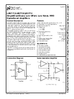
LMV771/LMV772/LMV774
Single/Dual/Quad, Low Offset, Low Noise, RRO
Operational Amplifiers
General Description
The LMV771/LMV772/LMV774 are Single, Dual, and Quad
low noise precision operational amplifiers intended for use in
a wide range of applications. Other important characteristics
of the family include: an extended operating temperature
range of −40°C to 125°C, the tiny SC70-5 package for the
LMV771, and low input bias current.
The extended temperature range of −40°C to 125°C allows
the LMV771/LMV772/LMV774 to accommodate a broad
range of applications. The LMV771 expands National
Semiconductor’s Silicon Dust™ amplifier portfolio offering en-
hancements in size, speed, and power savings. The LMV771/
LMV772/LMV774 are guaranteed to operate over the voltage
range of 2.7V to 5.0V and all have rail-to-rail output.
The LMV771/LMV772/LMV774 family is designed for preci-
sion, low noise, low voltage, and miniature systems. These
amplifiers provide rail-to-rail output swing into heavy loads.
The maximum input offset voltage for the LMV771 is 850
μ
V
at room temperature and the input common mode voltage
range includes ground.
The LMV771 is offered in the tiny SC70-5 package, LMV772
in the space saving MSOP-8 and SOIC-8, and the LMV774
in TSSOP-14.
Features
(Unless otherwise noted, typical values at V
S
= 2.7V)
■
Guaranteed 2.7V and 5V specifications
■
Maximum V
OS
(LMV771)
850μ
V (limit)
■
Voltage noise
—
f = 100Hz
12.5nV/
—
f = 10kHz
7.5nV/
■
Rail-to-Rail output swing
—
R
L
= 600Ω
100 mV from rail
—
R
L
= 2k
Ω
50 mV from rail
■
Open loop gain with R
L
= 2k
Ω
100 dB
■
V
CM
0 to V
+
-0.9V
■
Supply current (per amplifier)
550 µA
■
Gain bandwidth product
3.5 MHz
■
Temperature range
−40°C to 125°C
Applications
■
Transducer amplifier
■
Instrumentation amplifier
■
Precision current sensing
■
Data acquisition systems
■
Active filters and buffers
■
Sample and hold
■
Portable/battery powered electronics
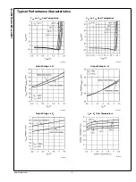
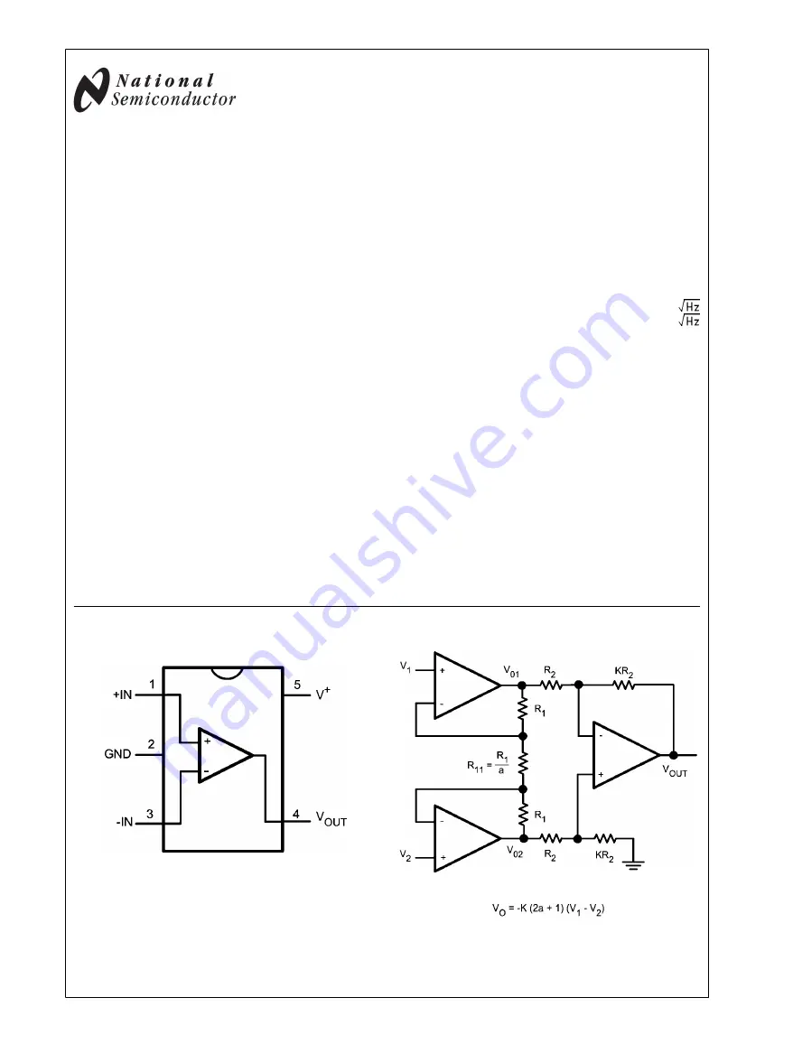
Connection Diagram
SC70-5
20039667
Top View
Instrumentation Amplifier
20039636
Silicon Dust
™
is a trademark of National Semiconductor Corporation.
© 2007 National Semiconductor Corporation
200396
www.national.com
LMV771/LMV772/LMV774 Single/Dual/Quad, Low Offset, Low Noise, RRO Operational Amplifiers


