


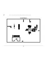
L M X 2 5 3 1 L Q 1 2 2 6 E E V A L U A T I O N B O A R D O P E R A T I N G I N S T R U C T I O N S
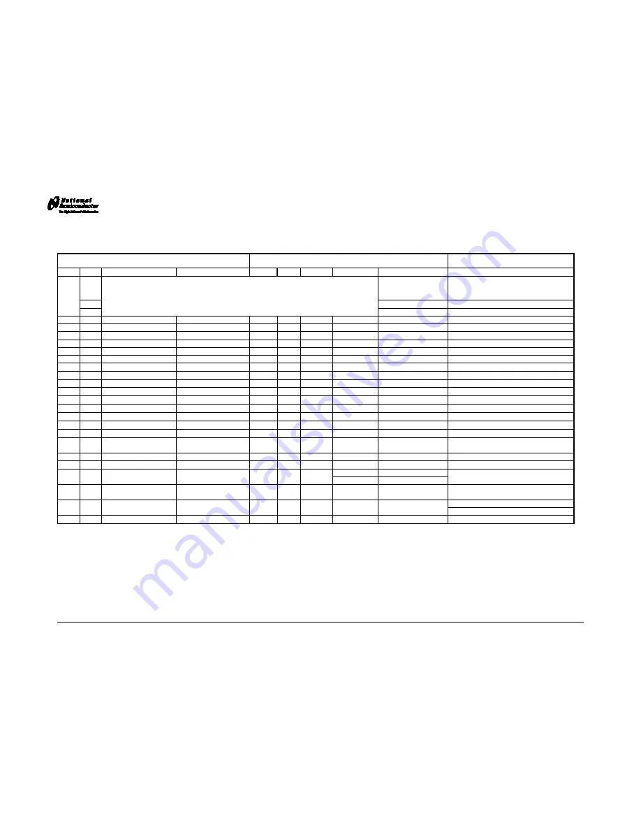
Bill of Materials
Bill of Materials
LMX2531_LF
Revision 3.28.2008
Item
QTY
Manufacturer
Part
#
Size
Tol
Voltage
Material
Value
Designators
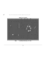
C1_LF, C2pLF, C2, C3, C4, C5, C9,
C11, C14, C17, C18, C19, C21, C24,
20
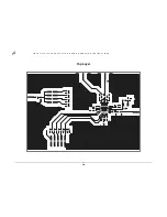
Open Capacitors
C100, C101, C102, C103, C104, C105
7
Open Resistors
R2pLF,R7, R8, R17, R19, R21, R24
0
1
n/a
Open Miscellaneous
Ftest/LD
1
1
Kemet
C0603C101J5GAC
603
5%
50V
C0G
100pF
C16
2
2
Kemet
C0603C103J5RAC
603
5%
50V
X7R
10nF
C10, C23
3
1
Kemet
C0805C104K5RACTU
805
5%
25V
C0G
100nF
C2_LF
4
6
Kemet
C0603C104J3RAC
603
5%
25V
X7R
100nF
C6, C7, C12, C15, C22, C20
5
1
Kemet
C0603C105K4RAC
603
10%
16V
X5R
1uF
C8
6
1
Kemet
C0603C475K9PAC
603
10%
6.3V
X5R
4.7uF
C13
7
1
Kemet
C0805C106K8PAC
805
10%
10V
X5R
10uF
C1
8
1
Vishay
CRCW0603000ZRT1
603
5%
0.1W
Thick
Film
0
Ω
R20
9
2
Panasonic
P.22AHCT-ND 603
10%
0.1W
Thick
Film
0.22
Ω
R22, R23
10
2
Vishay
CRCW06033R3JRT1
603
5%
0.1W
Thick
Film
3.3
Ω
R1, R18
11
4
Vishay
CRCW0603100JRT1
603
5%
0.1W
Thick
Film
10
Ω
R2, R3, R4, R5
12
1
Vishay
CRCW0603510JRT1
603
5%
0.1W
Thick
Film
51Ω
R6
13
1
Vishay
CRCW0603102JRT1
603
5%
0.1W
Thick
Film
1K
Ω
R2_LF
14
4
Vishay
CRCW0603103JRT1
603
5%
0.1W
Thick
Film
10K
Ω
R9, R11, R13, R15
15
4
Vishay
CRCW0603123JRT1
603
5%
0.1W
Thick
Film
12K
Ω
R10, R12, R14, R16
16
1
Comm Con
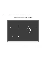
Connectors
HTSM3203-8G2
2X4
n/a
n/a
Metal/Plastic
Header
POWER
17
1
FCI
Electronics
52601-S10-8
2X5
n/a
n/a
Metal/Plastic
Header
uWire
18
3
Johnson Components
142-0701-851
SMA
n/a
n/a
Metal
SMA
Fout, OSCin, Vcc
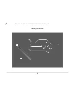
FR4
PCB
Board
19
1
National
Semiconductor
LMX2531LQEBPCB
n/a
n/a
n/a
62 mil Thick
1st Layer 10 mils
n/a
20
1
National
Semiconductor
LMX2531
LLP36
n/a
2.7
Silicon
LMX2531
U1
Place Across:
21
4
Com Con Connectors
CCIJ255G
2-Pin
n/a
n/a
Metal/Plastic
Shunt
POWER: 1-2, 3-4, 5-6, 7-8
22
4
SPC
Technology
SPCS-8
0.156"
n/a
n/a
Nylon
Nylon
Standoffs
Place in 4 Holes in Corners of Board
18


