background image

Nations Technologies Inc.

Tel

+86-755-86309900

Email

info@nationstech.com

Address: Nations Tower, #109 Baoshen Road, Hi-tech Park North. 
Nanshan District, Shenzhen, 518057, P.R.China


618

 / 

631


Bit Field 

Name 

Description 

1


Software can only read this bit, not write this bit. 

2


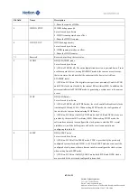
When multiple endpoint requests are interrupted at the same time, the hardware 

writes the endpoint number with the highest priority. Isochronous endpoints and 

double-buffered bulk endpoints have high priority, other endpoints have low 

priority (the lower the endpoint number, the higher the priority). 


USB frame number register (USB_FN) 

Address offset: 0x48 

Reset value: 0x0000 0XXX, X stands for undefined value 


Bit Field 

Name 

Description 

31:16 

Reserved 

Reserved, the reset value must be maintained.   

15 

RXDP_STS 

D+ status 

Represents the state of the USB D+ line, and can detect the occurrence of a resume 

condition in the suspend state. 

14 

RXDM_STS 

D- status 

Represents the state of the USB D- line, and can detect the occurrence of a resume 

condition in the suspend state. 

13 

LOCK 

Lock USB 

This bit is set by hardware if at least 2 PID SOF token packets are detected 

continuously after the end of an USB reset condition or after the end of an USB 

resume sequence. 

Note: 

1


When USB_FN.LOCK = 1, the frame counter will stop counting before the USB 

module is reset or the USB bus is suspended.


12:11 

LSTSOF[1:0] 

Lost SOF flag 

The hardware increments this bit every time the USB_STS.ESOF event occurs, and 

once the PID SOF token packet is received, the hardware clears this bit. 

10:0 

FNUM[10:0] 

Number of frames 

Hardware increments this bit every time the USB module receives a PID SOF token 

packet. 

Summary of Contents for N32G43 Series

Page 1: ...N32G43x series 32 bit ARM Cortex M4F microcontroller User manual V2 0 ...

Page 2: ...er modes 35 RUN mode 37 SLEEP mode 38 LOW POWER RUN mode 39 LOW POWER SLEEP mode 40 STOP2 mode 40 STANDBY mode 41 Low power auto wakeup AWU mode 42 PWR registers 43 PWR register overview 43 Power control register 1 PWR_CTRL1 43 Power control register 2 PWR_CTRL2 44 Power control register 3 PWR_CTRL3 45 Power status register 1 PWR_STS1 47 Power status register 1 PWR_STS1 48 Power status clear regis...

Page 3: ...earing 94 External interrupt wake up line 95 Alternate function 95 IO configuration of peripherals 105 GPIO locking mechanism 107 GPIO registers 108 GPIO registers overview 108 GPIO mode description register GPIOx_PMODE 109 GPIO type definition GPIOx_POTYPE 110 GPIO port slew rate configuration register GPIOx_SR 110 GPIO pull up pull down description register GPIOx_PUPD 111 GPIO input data registe...

Page 4: ...ress incrementation 137 Channel configuration procedure 137 Flow control 138 Circular mode 139 Error management 139 Interrupt 139 DMA request mapping 140 DMA registers 141 DMA register overview 141 DMA interrupt status register DMA_INTSTS 143 DMA interrupt flag clear register DMA_INTCLR 144 DMA channel x configuration register DMA_CHCFGx 144 DMA channel x transfer number register DMA_TXNUMx 146 DM...

Page 5: ... 199 Control register 2 TIMx_CTRL2 201 Slave mode control register TIMx_SMCTRL 203 DMA Interrupt enable registers TIMx_DINTEN 206 Status registers TIMx_STS 207 Event generation registers TIMx_EVTGEN 209 Capture compare mode register 1 TIMx_CCMOD1 210 Capture compare mode register 2 TIMx_CCMOD2 213 Capture compare enable registers TIMx_CCEN 215 Counters TIMx_CNT 218 Prescaler TIMx_PSC 218 Auto relo...

Page 6: ...MOD1 269 Capture compare mode register 2 TIMx_CCMOD2 272 Capture compare enable registers TIMx_CCEN 274 Counters TIMx_CNT 275 Prescaler TIMx_PSC 276 Auto reload register TIMx_AR 276 Capture compare register 1 TIMx_CCDAT1 276 Capture compare register 2 TIMx_CCDAT2 277 Capture compare register 3 TIMx_CCDAT3 277 Capture compare register 4 TIMx_CCDAT4 278 DMA Control register TIMx_DCTRL 278 DMA transf...

Page 7: ... counter register LPTIM_CNT 312 Real time clock RTC 314 Introduction 314 Main feature 314 Function description 316 RTC block diagram 316 GPIO controlled by RTC 317 RTC register write protection 317 RTC clock and prescaler 317 RTC calendar 318 Calendar initialization and configuration 318 Calendar reading 319 Calibration clock output 320 Programmable Alarm 320 Alarm configuration 320 Alarm output 3...

Page 8: ...egister access protection 346 Debugging mode 347 User interface 347 Operate flow 347 IWDG configuration flow 348 IWDG registers 348 IWDG register overview 348 IWDG key register IWDG_KEY 349 IWDG pre scaler register IWDG_PREDIV 349 IWDG reload register IWDG_RELV 350 IWDG status register IWDG_STS 350 Window watchdog WWDG 352 Introduction 352 Main features 352 Function description 352 Timing for refr...

Page 9: ...ster 3 ADC_RSEQ3 381 ADC Injection sequence register ADC_JSEQ 382 ADC injection data register x ADC_JDATx x 1 4 382 ADC regulars data register ADC_DAT 383 ADC differential mode selection register ADC_DIFSEL 383 ADC calibration factor ADC_CALFACT 384 ADC control register 3 ADC_CTRL3 384 ADC sampling time register 3 ADC_SAMPT3 386 Digital to analog conversion DAC 386 Introduction 386 Main features 3...

Page 10: ...TS 413 Operational Amplifier OPAMP 414 Main features 414 OPAMP function description 414 OPAMP working mode 415 OPAMP independent op amp mode 415 OPAMP follow mode 416 OPAMP internal gain PGA mode 417 OPAMP with filtered internal gain mode 418 OPAMP calibration 419 OPAMP Independent write protection 419 OPAMP TIMER controls the switching mode 419 OPAMP register 419 OPAMP register overview 419 OPAMP...

Page 11: ...1 USART Status register USART_STS 482 USART Data register USART_DAT 484 USART Baud rate register USART_BRCF 485 USART control register 1 register USART_CTRL1 485 USART control register 2 register USART_CTRL2 487 USART control register 3 register USART_CTRL3 488 USART guard time and prescaler register USART_GTP 490 Low power universal asynchronous receiver transmitter LPUART 492 Introduction 492 Ma...

Page 12: ...ol register 1 SPI_CTRL1 not used in I2S mode 541 SPI control register 2 SPI_CTRL2 543 SPI status register SPI_STS 544 SPI data register SPI_DAT 545 SPI CRC polynomial register SPI_CRCPOLY not used in I2 S mode 546 SPI RX CRC register SPI_CRCRDAT not used in I2 S mode 546 SPI TX CRC register SPI_ CRCTDAT 546 SPI_I2 S configuration register SPI_I2SCFG 547 SPI_I2S prescaler register SPI_I2SPREDIV 548...

Page 13: ...ndpoint n register USB_EPn n 0 7 611 USB control register USB_CTRL 614 USB interrupt status register USB_STS 616 USB frame number register USB_FN 618 USB device address register USB_ADDR 619 USB packet buffer description table address register USB_BUFTAB 619 Buffer description table 619 Send buffer address register n USB_ADDRn_TX 620 Send data byte number register n USB_CNTn_TX 620 Receive buffer ...

Page 14: ...on remapping 96 Table 5 5 ADC external trigger regular conversion alternate function remapping 97 Table 5 6 TIM1 alternate function remapping 97 Table 5 7 TIM2 alternate function remapping 97 Table 5 8 TIM3 alternate function remapping 98 Table 5 9 TIM4 alternate function remapping 98 Table 5 10 TIM5 alternate function remapping 98 Table 5 11 TIM8 alternate function remapping 98 Table 5 12 TIM9 al...

Page 15: ...rs overview 108 Table 5 43 AFIO register overview 116 Table 6 1 Vector table 122 Table 6 2 EXTI register overview 129 Table 7 1 Programmable data width and endian operation when PINC MINC 1 136 Table 7 2 Flow control table 138 Table 7 3 DMA interrupt request 139 Table 7 4 DMA request mapping 140 Table 7 5 DMA register overview 141 Table 8 1 CRC register overview 153 Table 10 1 Counting direction v...

Page 16: ...ed for external triggering of injection channels 369 Table 17 7 ADC interrupt 371 Table 17 8 ADC register overview 371 Table 18 1 DAC pins 388 Table 18 2 DAC external trigger 390 Table 18 3 DAC registers overview 394 Table 19 1 COMP register overview 403 Table 20 1 OPAMP register overview 419 Table 21 1 Comparison between SMBus and I2C 438 Table 21 2 I2C interrupt request 440 Table 21 3 I2C regist...

Page 17: ...ble 25 2 Send mailbox register list 564 Table 25 3 Receive mailbox register list 565 Table 25 4 CAN register overview 572 Table 26 1 DATTOG and SW_BUF definitions 601 Table 26 2 How to use double buffering 601 Table 26 3 How to use isochronous double buffering 607 Table 26 4 Resume event detection 609 Table 26 5 USB register overview 610 Table 26 6 Receive status code 613 Table 26 7 Send status co...

Page 18: ...iagram of TIM1 and TIM8 159 Figure 10 2 Counter timing diagram with prescaler division change from 1 to 4 160 Figure 10 3 Timing diagram of up counting The internal clock divider factor 2 N 162 Figure 10 4 Timing diagram of the up counting update event when ARPEN 0 1 163 Figure 10 5 Timing diagram of the down counting internal clock divided factor 2 N 165 Figure 10 6 Timing diagram of the Center a...

Page 19: ... 197 Figure 11 1 Block diagram of TIMx x 2 3 4 5 and 9 228 Figure 11 2 Counter timing diagram with prescaler division change from 1 to 4 229 Figure 11 3 Timing diagram of up counting The internal clock divider factor 2 N 231 Figure 11 4 Timing diagram of the up counting update event when ARPEN 0 1 232 Figure 11 5 Timing diagram of the down counting internal clock divided factor 2 N 233 Figure 11 6...

Page 20: ...filter timing diagram 295 Figure 13 3 LPTIM output waveform Continuous counting mode configuration 296 Figure 13 4 PTIM output waveform single counting mode configuration 297 Figure 13 5 LPTIM output waveform Single counting mode configuration and One time mode activated 298 Figure 13 6 Waveform generation 299 Figure 13 7 Encoder mode counting sequence 302 Figure 13 8 Input waveforms of Input1 and...

Page 21: ...am 432 Figure 21 6 Master receiver transfer sequence diagram 434 Figure 22 1 USART block diagram 455 Figure 22 2 Word length 8 setting 456 Figure 22 3 Word length 9 setting 457 Figure 22 4 Configuration stop bit 458 Figure 22 5 TXC TXDE changes during transmission 459 Figure 22 6 Start bit detection 460 Figure 22 7 Transmission using DMA 466 Figure 22 8 Reception using DMA 467 Figure 22 9 Hardware...

Page 22: ...MODE 0 and RONLY 1 518 Figure 24 8 Schematic diagram of the change of TE RNE BUSY when the slave is continuously transmitting in full duplex mode 518 Figure 24 9 Schematic diagram of TE BUSY change during continuous transmission in slave unidirectional transmit only mode 519 Figure 24 10 Schematic diagram of TE BUSY change when BIDIRMODE 0 and RONLY 0 are transmitted discontinuously 521 Figure 24 ...

Page 23: ...59 Figure 25 8 Receive FIFO status 560 Figure 25 9 Filter bit width setting register organization 562 Figure 25 10 Examples of filter mechanisms 564 Figure 25 11 Bit sequence 566 Figure 25 12 Various CAN frames 567 Figure 25 13 Event flag and interrupt generation 568 Figure 25 14 CAN error state diagram 569 Figure 26 1 USB device block diagram 597 Figure 26 2 The user applications on the microcont...

Page 24: ... no effect on this bit read clear rc_w0 Software can read this bit or clear it by writing 0 and writing 1 has no effect on this bit read clear by read rc_r Software can read this bit Reading this bit will automatically clear it to 0 Writing 0 has no effect on this bit read set rs Software can read or set this bit Writing 0 has no effect on this bit read only write trigger rt_w Software can read th...

Page 25: ...interface Instruction prefetching is completed on this bus Core Cortex M4FP Fmax 108MHz AHB Bus Matrix Max 108MHz Flash Control Flash DCode TPIU SW JTAG NVIC FPU DSP SBus ICode DMA DMA ADC iCache SRAM SAC RCC CRC APB2 Max 54MHz APB1 Max 27MHz EXTI GPIOA GPIOB GPIOC GPIOD GPIOE GPIOF USART1 UART4 UART5 SPI1 I2S1 SPI2 I2S2 AFIO EXTI GPIOA GPIOB GPIOC GPIOD TIM1 TIM8 AFIO GPIOA GPIOB GPIOC GPIOE COMP...

Page 26: ... two AHB2APB Bridges i e AHB2APB1 and AHB2APB2 The maximum speed of APB1 PCLK is 27MHz the maximum speed of APB2 PCLK is 54MHz Bus address mapping The address mapping includes all AHB and APB peripherals AHB peripherals APB1 peripherals APB2 peripherals Flash SRAM System Memory etc And the address space of SRAM is located in the bit band Region of SRAM and atomic accesses can be made through the b...

Page 27: ... 0xE000_2FFF 0xE000_1000 0xE000_1FFF 0xE000_0000 0xE000_0FFF Reserved ROM Table External PPB ETM TPIU 0xE010_0000 0xFFFF_FFFF 0xE00F_F000 0xE00F_FFFF 0xE004_2000 0xE00F_EFFF 0xE004_1000 0xE004_1FFF 0xE004_0000 0xE004_0FFF COMP OPAMP Reserved Reserved TIM7 TIM6 TIM5 TIM4 TIM3 TIM2 0x4000_2400 0x4000_27FF 0x4000_2000 0x4000_23FF 0x4000_1C00 0x4000_1FFF 0x4000_1800 0x4000_1BFF 0x4000_1400 0x4000_17FF...

Page 28: ...001_1400 0x4001_17FF GPIOD 0x4001_1000 0x4001_13FF GPIOC 0x4001_0C00 0x4001_0FFF GPIOB 0x4001_0800 0x4001_0BFF GPIOA 0x4001_0400 0x4001_07FF EXTI 0x4001_0000 0x4001_03FF AFIO 0x4000_7800 0x4000_FFFF Reserved APB1 0x4000_7400 0x4000_77FF DAC 0x4000_7000 0x4000_73FF PWR 0x4000_6800 0x4000_6FFF Reserved 0x4000_6400 0x4000_67FF CAN 0x4000_6000 0x4000_63FF USB SRAM 512B 0x4000_5C00 0x4000_5FFF USB Regi...

Page 29: ...ation to be performed The following mapping formula shows how each byte in the alias area corresponds to the corresponding bit in the bit band area bitband_ byte _addr bitband _base byte_offset 32 bit_number 4 In which bitband_byte_addr is the address of the byte in the alias memory area which is mapped to a certain target bit bitband _base is the starting address of alias area byte_offset is the ...

Page 30: ...FFF_0000 ICode DCode DMA Boot from the built in SRAM The built in SRAM is mapped to boot space 0x0000_0000 The built in SRAM is accessible in two address areas 0x0000_0000 or 0x2000_0000 ICode DCode SBus DMA Boot configuration In addition SRAM can also be accessed through virtual address segment 0x1000_0000 which makes the CPU jump to SRAM to run programs through ICode DCode after starting from Ma...

Page 31: ...ess space Data bytes are stored in the memory in little endian format The lowest address byte in a word is regarded as the least significant byte of the word while the highest address byte is the most significant byte The specifications of program memory and data memory are as follows FLASH specification Flash consists of a main storage area and an information area which are described separately b...

Page 32: ...FLASH_ECC 0x4002_2024 0x4002_2027 4B Reserved 0x4002_2028 0x4002_202F 8B FLASH_CAHR 0x4002_2030 0x4002_2033 4B Flash memory is organized into 32 bit wide memory units which can store codes and data constants Information is divided into three parts The system memory area is used for storing a boot program for boot loader mode of the system memory The boot program uses USART1 and USB DFU serial inte...

Page 33: ...d that FLASH_CTRL LATENCY is greater than 2 at least 3 wait periods Sleep Mode configure the FLASH_CTRL SLMEN bit to enable this mode In sleep mode code cannot be run in Flash only in SRAM Unlock Flash After reset the Flash module is protected and cannot be written into the FLASH_CTRL register to prevent accidental operation of Flash due to electrical interference and other reasons By writing a sp...

Page 34: ...rations in progress Set the FLASH_CTRL PG bit to 1 Write the word to be programmed at the specified address Wait for the FLASH_ STS BUSY bit to change to 0 Read the written address and verify the data Note When the FLASH_STS BUSY bit is 1 you cannot write to any register 2 2 1 4 3 Option byte erase and programming The option byte area is programmed differently from the main storage area The number...

Page 35: ...tection software hardware watchdog configuration boot management BOR gear selection and reset options when the system is in standby stop2 mode and bus address space is allocated for read write access They consist of byte with 10 options 4 byte for write protection 2 bytes for read protection 2 byte for configuration option 2 bytes defined by user These 10 bytes need to be written through the bus T...

Page 36: ...P0 0x1FFF_F80C nWRP3 WRP3 nWRP2 WRP2 0x1FFF_F810 nUSER2 USER2 nRDP2 RDP2 Read protection L1 level option byte RDP1 Protect the code stored in the flash memory When the correct value is written it will be forbidden to read the flash memory The result of whether RDP1 is turned on or not can be inquired through FLASH_OB 1 User configuration options USER USER 7 3 Reserved USER 2 nRST_STDBY configurati...

Page 37: ...erence The basic unit of write protection is for Page0 63 every 2 pages is a basic protection unit Write protection can be configured by setting WRP0 3 in the option byte block After each configuration A system reset is required for the configured value to be reloaded to take effect If an attempt is made to program or erase a protected page a protection error flag will be returned in the FLASH_STS...

Page 38: ...er pages can be programmed by the code executed in the main flash memory realizing IAP or data storage and other functions All pages are not allowed to write or erase in debug mode or after booting from internal SRAM except for mass erase All functions of loading code into the built in SRAM through JTAG SWD and then execute it are still valid or they can be started from the built in SRAM through J...

Page 39: ... 0xCC nRDP2 0x33 it is L2 level Table 2 6 Flash read write erase 1 permission control table protect level Boot mode Main Flash Changing a Protection Level Perform user Access area JTAG SWD Main Flash System Memory SRAM L0 level Before 4KB of flash main memory area Read Write Erase Read Write Erase Read Write Erase Read Write Erase Change to L1 or L2 is allowed After 4KB of flash main memory area R...

Page 40: ... is allowed After 4KB of flash main memory area Read write erase Read write erase Read write erase Flash main memory area mass erase Allow Allow Allow Flash option byte area Read only Read only Read only Flash system memory area Prohibit Read write erase Prohibit SRAM All Read and write Read and write Read and write protect level Boot mode SRAM Changing a Protection Level Perform user Access to ar...

Page 41: ... is allowed When changed to L0 the main memory area is automatically erased After 4KB of flash main memory area Prohibit Read write erase Read write erase Prohibit Flash main memory area mass erase Allow Allow Allow Allow Flash option byte area Read write erase Read write erase Read write erase Read write erase Flash system memory area Prohibit Prohibit Prohibit Prohibit SRAM All Read and write Re...

Page 42: ...ow Allow Allow Allow Flash option byte area Read write erase Read write erase Read write erase Read write erase Flash system memory area Prohibit Prohibit Read write erase Prohibit SRAM All Read and write Read and write Read and write Read and write L1 level Before 4KB of flash main memory area Prohibit Read only Read only Read only L0 or L2 is allowed When changed to L0 the main memory area is au...

Page 43: ... efficiency Because of the existence of the instruction buffer the CPU will be able to work at a higher frequency When the instruction requested by the CPU is in the instruction buffer the CPU can obtain the instruction without delay and realize zero waiting for execution When the current instruction sequence instruction prefetch sequence and instruction buffer all miss Flash will be re read and t...

Page 44: ...he must be closed and the data of the iCache must be cleared otherwise the instruction acquisition error will occur 2 2 2 3 2 iCache data refresh The iCache is designed as instruction cache When the instruction is updated by application software or the instruction jumps between the main memory area and other memory areas the software must set the FLASH_AC ICAHRST bit to 1 to clear the data in the ...

Page 45: ...Code and DCode and can run programs at full speed in SRAM The maximum address range of SRAM is 0x2000 0000 0x2000 7FFF In Stop2 mode SRAM1 and SRAM2 data optional retention in STANDBY mode only SRAM2 data optional rentention The main features are as follows The maximum capacity is 32KB in total Support byte half word word reading and writing I D S DMA can be accessed I D BUS can run programs at fu...

Page 46: ... 1 0 0 0 01Ch FLASH_OB RDPRT2 Reserved Data1 Data0 Not Used nRST_STDBY nRST_STOP2 WDG_SW RDPRT1 OBERR Reset Value 0 1 1 1 1 1 1 1 1 1 1 1 1 1 1 1 1 1 1 1 1 1 1 1 1 0 0 020h FLASH_WRP WRPT Reset Value 1 1 1 1 1 1 1 1 1 1 1 1 1 1 1 1 1 1 1 1 1 1 1 1 1 1 1 1 1 1 1 1 024h FLASH_ECC Reserved ECCHW Reserved ECCLW Reset Value 0 0 0 0 0 0 0 0 0 0 0 0 028h 02Ch Reserved 030h FLASH_CAHR Reserved LOCKSTOP LO...

Page 47: ...king mode 7 ICAHEN iCache enable 0 Turn off iCache 1 Enable iCache 6 ICAHRST iCache reset 0 Writing 0 is invalid 1 Write 1 to reset 5 PRFTBFS Prefetch buffer status This bit indicates the status of the prefetch buffer 0 The prefetch buffer is closed 1 The prefetch buffer is open 4 PRFTBFE Prefetch buffer enable 0 Close the prefetch buffer 1 Enable prefetch buffer 3 Reserved Reserved the reset valu...

Page 48: ...lock the FLASH_CTRL OPTWE bit 2 2 4 2 4 The FLASH status register FLASH_STS Address offset 0x0C Reset value 0x0000 0000 Bit field Name Description 31 8 Reserved Reserved the reset value must be maintained 7 ECCERR ECC error Read FLASH error hardware set this bit to 1 write 1 to clear this state 6 EVERR Erase check error When the page is erased and the check reports an error the hardware sets this ...

Page 49: ...re programming the FLASH_CTRL START bit must be cleared 1 Reserved Reserved the reset value must be maintained 0 BUSY Busy This bit indicates that a flash operation is in progress At the beginning of flash operation this bit is set to 1 This bit is cleared to 0 when the operation ends or an error occurs 2 2 4 2 5 The FLASH control register FLASH_CTRL Address offset 0x10 Reset value 0x0000 0080 Bit...

Page 50: ...ation will not be performed and the FLASH_STS PGERR warning bit will be set 1 SMP2 mode Before programming it will not judge whether the content of the address where the programming is located has been erased and the Flash will directly start programming If the programming address has been written with data before only the same data can be written when programming the address in SMP2 mode otherwis...

Page 51: ...ess register FLASH_ADD Address offset 0x14 Reset value 0x0000 0000 Bit field Name Description 31 0 FADD Flash address Select the address to be programmed when programming and select the page to be erased when page erasing Note When the FLASH_STS BUSY bit is 1 this register cannot be written 2 2 4 2 7 The FLASH Option byte register 2 FLASH_OB2 Address offset 0x18 Reset value 0x0c800000 Bit field Na...

Page 52: ...ot Management 2 2 4 2 8 Option byte register FLASH_OB Address offset 0x1C Reset value 0x03FF FFFC Bit field Name Description 31 RDPRT2 Read protection L2 level protection 0 Read protection L2 level is not enabled 1 Read protection L2 level is enabled Note This bit is read only 30 26 Reserved Reserved the reset value must be maintained 25 18 Data1 7 0 Data1 Note This bit is read only 17 10 Data0 7 ...

Page 53: ...protection L1 level is not enabled 1 Read protection L1 level is enabled Note This bit is read only 0 OBERR Option byte error When this bit is 1 it means that the option byte does not match its complement Note This bit is read only 2 2 4 2 9 Write protection register FLASH_WRP Address offset 0x20 Reset value 0xFFFF FFFF Bit field Name Description 31 0 WRPT Write protect This register contains the ...

Page 54: ...responding higher 6 bit ECC value 7 6 Reserved Reserved the reset value must be maintained 5 0 ECCLW After writing a word to a 32 bit Flash address the corresponding lower 6 bit ECC value 2 2 4 2 11 CAHR register FLASH_CAHR Address offset 0x30 Reset value 0x0000 0000 Bit field Name Description 31 8 Reserved Reserved the reset value must be maintained 7 4 LOCKSTOP 3 0 iCache lock stop see for detai...

Page 55: ... supply VDDA domain The voltage input range is 1 8V 3 6V which mainly supplies power for most analog peripherals A D D A TS Temperature Sensor and OPAMP are in this power domain This independent analog power supply is powered by VSSA which can filter and shield noise separately and improve the conversion accuracy performance of analog modules such as A D and D A VREF or VREF domain External VREF V...

Page 56: ...the option byte During power on the BOR will hold the chip in reset until the supply voltage VDD reaches the specified threshold When VDD falls below the selected threshold the chip will be reset For more information on switching power supply reset thresholds see the Electrical Characteristics section of the relevant data sheet VDD TS VSSA HSE HSI PLL OSC300M DAC ADC COMP OPA IO rings except PC13 ...

Page 57: ...R_CTRL2 PVDEN The PWR_STS2 PVDO flag is used to indicate whether the VDD is above below the PVD voltage threshold This event is connected internally to the 16th line of the external interrupt and produces an interrupt if the interrupt is enabled in the external interrupt register APVD interrupt occurs when the VDD drops below the PVD threshold and or when the VDD rises above the PVD threshold acco...

Page 58: ...ower wake up Enter another power mode Code execution continues without peripheral reconfiguration SLEEP MR 1 WFI returned from ISR 2 WFE any interrupt or wake up event Code execution continues without peripheral reconfiguration LOW POWER RUN LPR By configuring PWRCTRL1 LPREN bit Clear PWRCTRL1 LPREN bit or system reset Code execution continues without peripheral reconfiguration LOW POWER SLEEP LPR...

Page 59: ...p the code can continue running from the stop position The RCC configuration is retained and the SPI UART2 UART3 UART4 UART5 I2C1 I2C2 WWDG configuration is retained 2 Please refer to the corresponding data sheet for the low power wake up time The running enable conditions of different modules in different power consumption modes are shown in the following table Table 3 2 Blocks running state Main...

Page 60: ...R O O CAN O O O O SAC O O CRC O O O O DAC O O O O ADC O O O O TempSensor O O O O OPAMP O O O O COMP O O O O O Y TRNG O O GPIOs O O O O O Y O 3 pins Note 1 Y Yes Enable O Option Not available 2 Only COMP1 support STOP2 mode 3 3 pins represent three wake up IOs PA8 PA0 and PC13 RUN mode RUN mode is the normal operation mode of the MCU The speed of the system clock can be reduced by configuring the R...

Page 61: ... 0x2 then poll to wait for PWR_STS2 MRF to be pulled low and then pulled high It takes about 100us to pull down PWR_STS2 MRF Steps for MR1 0V MR 1 1V Configure PWR_CTRL1 MRSEL 1 0 0x3 then poll and wait for PWR_STS2 MRF to be pulled low and then pulled high It takes about 100us to pull down PWR_STS2 MRF Configure the FLASH read cycle to be greater than or equal to 2 This step is to avoid entering ...

Page 62: ...IC interrupt channel suspend bit in the NVIC interrupt clear suspend register because the suspend bit corresponding to the event line is not set This mode provides the shortest wake up time because there is no time spent on interrupt entry or exit LOW POWER RUN mode In LOW POWER RUN mode the entire core logic is provided by LPR and MR is disabled The system clock comes from MSI the frequency is up...

Page 63: ... the FLASH read delay to greater than 2 Clear FLASH_AC LVMEN and ensure that the FLASH low voltage mode is canceled by polling the FLASH_AC LVMF bit Restore the system clock to the required state Configure the FLASH read cycle according to the system clock and ensure that the read wait time is greater than or equal to 20ns for example 50MHz it can be configured to 0 LOW POWER SLEEP mode In LOW POW...

Page 64: ... be turned on by RCC_LDCTRL RTCEN Internal RC oscillator LSI RC optional It can be turned on by RCC_CTRLSTS LSIEN External 32 768kHz crystal oscillator LSE OSC optional It can be turned on by RCC_LDCTRL LSEEN bit Other peripherals that can choose to hold or work such as GPIO COMP EXTI LPUART LPTIMER IO can be configured to retention or high Z state Unneeded analog peripherals such as ADC and DAC c...

Page 65: ... event timestamp event tamper event occurs Except for the power status registers PWR_STS1 2 all registers are reset after waking up from STANDBY state After waking up from STANDBY mode code execution is the same as reset detecting BOOT pin getting reset vector etc The PWR_STS1 STBYF flag indicates that the MCU exits STANDBY mode Low power auto wakeup AWU mode In automatic wake up mode the RTC can ...

Page 66: ... Reserved PVDFLTEN PLS 2 0 PVDEN Reset Value 0 0 0 0 0 008h PWR_CTRL3 Reserved PSTSTP2 PSTSTBY Reserved PBDTSTBY PBDTSTP2 PBDTLPR Reserved IWKUPLEN RAM2RET RAM1RET Reserved BGDTSTBY BGDTSTP2 BGDTLPR Reserved WKUP2PS WKUP1PS WKUP0PS Reserved WKUP2EN WKUP1EN WKUP0EN Reset Value 0 0 1 1 1 0 0 0 1 1 1 0 0 0 0 0 0 00Ch PWR_STS1 Reserved IWKUPF Reserved STBYF Reserved WKUPF2 WKUPF1 WKUPF0 Reset Value 0 ...

Page 67: ...L register In the reset state the RTC backup registers and RCC_LDCTRL registers are protected from illegal writes This bit must be set to enable write access to these registers 0 Disable access to RTC backup registers and RCC_LDCTRL 1 Enable access to RTC backup registers and RCC_LDCTRL Note This bit must remain 1 if HSE is divided by 32 as the RTC clock 7 3 Reserved Reserved the reset value must ...

Page 68: ...PVD Power control register 3 PWR_CTRL3 Address offset 0x08 Reset value 0x0007 0700 reset by wakeup from STANDBY mode Bit field Name Description 31 22 Reserved Reserved the reset value must be maintained 21 PSTSTP2 Pin state bit in STOP2 mode 0 Pin in retention state 1 Pin in high Z state 20 PSTSTBY Pin state bit in STANDBY mode 0 Pin in retention state 1 Pin in high Z state 19 Reserved Reserved th...

Page 69: ...ays on 1 Duty on 9 BGDTSTP2 BANDGAP BG_Buffer IBIAS idle state bit in STOP2 mode 0 Always on 1 Duty on 8 BGDTLPR BANDGAP BG_Buffer IBIAS idle state bit in LP RUN mode 0 Always on 1 Duty on 7 Reserved Reserved the reset value must be maintained 6 WKUP2PS WKUP2 wake up pin polarity selection bit Use rising or falling edge to wake up STANDBY mode Make sure the corresponding wakeup pins are disabled b...

Page 70: ... on the WKUP pin will not wake the device from STANDBY mode 1 WKUP pin is used to wake up STANDBY mode Power status register 1 PWR_STS1 Address offset 0x0C Reset value 0x0000 0000 Power on reset or PWR soft reset clear Bit field Name Description 31 16 Reserved Reserved the reset value must be maintained 15 IWKUPF Internal wake up flag This bit is set and cleared by hardware 0 All internal wakeup s...

Page 71: ...nt received from WKUP pin Power status register 1 PWR_STS1 Address offset 0x10 Reset value 0x0000 0003 Power on reset or PWR soft reset clear Bit field Name Description 31 3 Reserved Reserved the reset value must be maintained 2 PVDO PVD output This bit is set and cleared by hardware Only valid when PWR_CTRL2 PVDEN 1 0 VDD VDDA is above the PVD threshold selected using PWR_CTRL2 PLS 2 0 1 VDD VDDA...

Page 72: ...31 9 Reserved Reserved the reset value must be maintained 8 CLRSTBY Clear STANDBY flag This bit always reads as 0 0 No effect 1 Clear PWR_STS1 STBYF flag 7 3 Reserved Reserved the reset value must be maintained 2 CLRWKUP2 Clear WKUP2 wakeup flag This bit always reads as 0 0 No effect 1 Clear wakeup flag PWR_STS1 WKUPF2 1 CLRWKUP1 Clear WKUP1 wakeup flag This bit always reads as 0 0 No effect 1 Cle...

Page 73: ...ers see Figure 3 1 The reset source in the figure will finally act on the NRST pin and remain low during the reset process System reset Except the reset flags in the Control Status Register RCC_CTRLSTS and the registers in the low power domain see Figure 3 1 a system reset sets all registers to their reset values A system reset is generated when one of the following events occurs A low level on th...

Page 74: ... entering STOP2 mode This reset is enabled by setting the nRST_STOP2 bit in the user option byte At this time even if the process to enter STOP2 mode is performed the system will be reset instead of entering STOP2 mode The system reset signal provided to the chip is output on the NRST pin The pulse generator guarantees a minimum reset pulse duration of 20μs for each reset source external or intern...

Page 75: ...o be selected by software to drive RTC LPTIMER LPUART Each clock source can be turned on or off independently when it is not used to optimize power consumption Several prescalers can be used to configure the frequencies of the AHB the high speed APB APB2 and the low speed APB APB1 domains The maximum frequencies of the AHB APB2 and APB1 domains are 108MHz 54MHz and 27MHz respectively RCC provides ...

Page 76: ... FCLK CPU AHB BUS HCLK 8 SysTick SAC_CLK CRC_CLK DMA_CLK APB1 Prescaler 1 2 4 8 16 27MHz MAX PCLK1 to APB1 peripherals 54MHz MAX PCLK2 to APB2 peripherals TIM 2 3 4 5 6 7 9 If APB1 Prescaler 1 x1 else x2 TIM2 3 4 5 6 7 9_CLK TIM1 8_CLK RTCSEL RTC_CLK to RTC IWDG_CLK SYSCLK LSI HSE MSI LSE LSI MCO PLLCLK Clock Tree MCO OSC32_IN OSC32_OUT OSC_IN OSC_OUT Legend HSE High speed external clock signal HS...

Page 77: ...HSE crystal The 4 to 32 MHz external oscillator has the advantage of producing a more accurate master clock for the system The associated hardware configuration is shown in See Figure 4 3 For more details please refer to the electrical characteristics section of the datasheet The RCC_CTRL HSERDF bit indicates whether the high speed external oscillator is stable or not At startup the clock is not r...

Page 78: ...m reset or wake up from STANDBY mode the MSI clock is used as the system clock and the MSI frequency is set to its default value of 4 MHz The RCC_CTRLSTS MSIRD bit indicates whether the MSI is stable The MSI output clock cannot be used until the hardware sets this bit to 1 at startup MSI can be turned on or off with the RCC_CTRLSTS MSIEN bit If the HSE crystal oscillator fails the MSI clock will b...

Page 79: ...onnected to the OSC32_IN pin while the OSC32_OUT pin must be left floating Hi Z LSI clock The LSI RC can clock the IWDG and AWU in STOP2 and STANDBY modes The LSI clock frequency is about 40kHz For further information please refer to the Electrical Characteristics section of the data sheet The LSI clock can be turned on or off using the RCC_CTRLSTS LSIEN bit The RCC_CTRLSTS LSIRD bit flag indicate...

Page 80: ...escue operations The CLKSSIF interrupt is connected to the NMI Non Maskable Interrupt interrupt of the Cortex M4 Once the CSS is activated and the HSE clock fails the CSS interrupt is generated and the NMI is automatically generated The NMI will be executed continuously until the CSS interrupt pending bit is cleared Therefore it is necessary to clear the CSS interrupt by setting the RCC_CLKINT CLK...

Page 81: ...the RTC cannot continue to work If the HSE clock divided by 32 is used as the RTC clock When in Stop2 or Standby mode the RTC state is indeterminate Watchdog clock If the IWDG is started by either hardware option or software access the LSI oscillator will be forced ON and cannot be disabled After the LSI oscillator is stabilized the clock is provided to the IWDG Clock output MCO The microcontrolle...

Page 82: ...PRST OPAMPRST Reserved DACRST PWRRST Reserved CANRST UCDRRST USBRST I2C2RST I2C1RST Reserved USART3RST USART2RST Reserved WWDGRST Reserved TIM9RST Reserved COMPRST TIM7RST TIM6RST TIM5RST TIM4RST TIM3RST TIM2RST Reset Value 0 0 0 0 0 0 0 0 0 0 0 0 0 0 0 0 0 0 0 014h RCC_AHBPCLKEN Reserved ADCEN SACEN Reserved RNGCEN Reserved CRCEN Reserved FLITFEN Reserved SRAMEN Reserved DMAEN Reset Value 0 0 0 0...

Page 83: ...PUARTSEL 1 0 LPTIMSEL 2 0 Reset Value 0 0 0 0 0 0 0 0 0 038h Reserved 03Ch Reserved 040h RCC_PLLHSIPRE Reserved PLLSRCDIV PLLHSIPRE Reset Value 0 0 044h SRAM_PARITY _CTRLSTS Reserved ERR2STS ERR2RSTEN ERR2IEN ERR1STS ERR1RSTEN ERR1IEN Reset Value 0 0 0 0 0 0 Clock Control Register RCC_CTRL Address offset 0x00 Reset value 0x0000 0040 Bit Field Name Description 31 26 Reserved Reserved the reset valu...

Page 84: ...he stop2 or standby mode it is cleared by hardware This bit cannot be cleared when HSE is used directly or indirectly as the system clock 0 Disable HSE oscillator 1 Enable HSE oscillator 15 7 HSICAL 8 0 Internal high speed clock calibration value These bits are automatically initialized at startup 6 2 HSITRIM 4 0 Internal high speed clock correction value Written by software The values of these bi...

Page 85: ...le 1 frequency division factor 2 0101 MCO clock divided by 6 duty cycle 1 frequency division factor 2 0110 MCO clock divided by 7 duty cycle 1 frequency division factor 2 0111 MCO clock divided by 8 duty cycle 1 frequency division factor 2 1000 MCO clock divided by 2 duty cycle 50 1001 MCO clock divided by 4 duty cycle 50 1010 MCO clock divided by 6 duty cycle 50 1011 MCO clock divided by 8 duty c...

Page 86: ...the RCC_APB1PCLKEN register 00 Divide the PLL clock by 1 5 as the USB clock 01 The PLL clock is directly used as the USB clock 10 Divide the PLL clock by 2 as the USB clock 11 Divide the PLL clock by 3 as the USB clock 21 18 PLLMULFCT 3 0 PLL multiplication factor including bit 27 Written by software to define PLL multiplication factor These bits can only be written when the PLL is disabled The PL...

Page 87: ...cleared by software to select PLL clock source This bit can only be written when PLL is disabled 0 HSI clock selected as PLL input clock 1 HSE clock selected as PLL input clock 15 14 Reserved Reserved the reset value must be maintained 13 11 APB2PRES 2 0 APB high speed APB2 prescaler Set and cleared by software to configure the division factor of APB2 clock PCLK2 Make sure that PCLK2 does not exce...

Page 88: ...om MSI 01 The system clock comes from HSI 10 The system clock comes from HSE 11 The system clock comes from the PLL output 1 0 SCLKSW 1 0 System clock switch Set and cleared by software to select the system clock source Set by hardware to force HSI selection when exiting from the stop2 or standby mode or when the HSE oscillator fails RCC_CTRL CLKSSEN is enabled 00 Select MSI as system clock 01 Sel...

Page 89: ...by the software to clear the CLKSSIF flag 0 No effect 1 Clear the CLKSSIF flag 22 Reserved Reserved the reset value must be maintained 21 BORICLR BOR interrupt clear This bit is set by software to clear the BORIF flag 0 No effect 1 BORIF cleared 20 PLLRDICLR PLL ready interrupt clear Set by the software to clear the PLLRDIF flag 0 No effect 1 Clear the PLLRDIF flag 19 HSERDICLR HSE ready interrupt...

Page 90: ... HSE ready interrupt 1 Enable HSE Ready Interrupt 10 HSIRDIEN HSI ready interrupt enable Set and cleared by software to enable and disable HSI ready interrupt 0 Disable HSI ready interrupt 1 Enable HSI ready interrupt 9 LSERDIEN LSE ready interrupt enable Set and cleared by software to enable and disable LSE ready interrupt 0 Disable LSE ready interrupt 1 Enable LSE ready interrupt 8 LSIRDIEN LSI ...

Page 91: ...setting the HSERDICLR bit 0 No clock ready interrupt caused by HSE oscillator 1 Clock ready interrupt caused by HSE oscillator 2 HSIRDIF HSI ready interrupt flag Set by hardware when HSIRDIEN is set and the HSI clock is ready This bit is cleared by software by setting the HSERDICLR bit 0 No clock ready interrupt caused by HSI oscillator 1 Clock ready interrupt caused by HSI oscillator 1 LSERDIF LS...

Page 92: ...T4 16 15 Reserved Reserved the reset value must be maintained 14 USART1RST USART1 reset Set and cleared by software 0 Clear the reset 1 Reset USART1 13 TIM8RST TIM8 timer reset Set and cleared by software 0 Clear the reset 1 Reset TIM8 timer 12 SPI1RST SPI1 reset Set and cleared by software 0 Clear the reset 1 Reset SPI1 11 TIM1RST TIM1 timer reset Set and cleared by software 0 Clear the reset 1 R...

Page 93: ...AMP interface reset Set or cleared by software 0 Clear the reset 1 Reset the OPAMP interface 30 Reserved Reserved the reset value must be maintained 29 DACRST DAC interface reset Set or cleared by software 0 Clear the reset 1 Reset the DAC interface 28 PWRRST Power interface reset Set and cleared by software 0 Clear the reset 1 Reset the power interface 27 26 Reserved Reserved the reset value must...

Page 94: ...ftware 0 Clear the reset 1 Reset I2C1 20 19 Reserved Reserved the reset value must be maintained 18 USART3RST USART3 reset Set or cleared by software 0 Cear the reset 1 Reset USART3 17 USART2RST USART2 reset Set and cleared by software 0 Clear the reset 1 Reset USART2 16 12 Reserved Reserved the reset value must be maintained 11 WWDGRST Window watchdog reset Set and cleared by software 0 Clear the...

Page 95: ...M5RST TIM5 timer reset Set and cleared by software 0 Clear the reset 1 Reset TIM5 timer 2 TIM4RST TIM4 timer reset Set and cleared by software 0 Clear the reset 1 Reset TIM4 timer 1 TIM3RST TIM3 timer reset Set and cleared by software 0 Clear the reset 1 Reset TIM3 timer 0 TIM2RST TIM2 timer reset Set and cleared by software 0 Clear the reset 1 Reset TIM2 timer AHB Peripheral Clock Enable Register...

Page 96: ...t and cleared by software 0 CRC clock disabled 1 CRC clock enabled 5 Reserved Reserved the reset value must be maintained 4 FLITFEN Flash interface circuit clock enable Set or cleared by software 0 Disable the clock of the flash interface circuit 1 Enable the clock of the flash interface circuit 3 Reserved Reserved 2 SRAMEN SRAM interface clock enable Set and cleared by software to disable enable ...

Page 97: ...tware 0 UART4 clock disabled 1 UART4 clock enabled 16 15 Reserved Reserved the reset value must be maintained 14 USART1EN USART1 clock enable Set and cleared by software 0 USART1 clock disabled 1 USART1 clock enabled 13 TIM8EN TIM8 Timer clock enable Set and cleared by software 0 TIM8 timer clock disabled 1 TIM8 timer clock enabled 12 SPI1EN SPI1 clock enable Set and cleared by software 0 SPI1 clo...

Page 98: ... Function IO clock disabled 1 Alternate Function IO clock enabled APB1 Peripheral Clock Enable Register RCC_APB1PCLKEN Address offset 0x1C Reset value 0x0000 0100 Bit Field Name Description 31 OPAMPEN OPAMP clock enable Set or cleared by software 0 Disable OPAMP clock 1 Enable OPAMP clock 30 Reserved Reserved the reset value must be maintained 29 DACEN DAC interface clock enable Set and cleared by...

Page 99: ... software 0 I2C2 clock disabled 1 I2C2 clock enabled 21 I2C1EN I2C1 clock enable Set and cleared by software 0 I2C1 clock disabled 1 I2C1 clock enabled 20 19 Reserved Reserved the reset value must be maintained 18 USART3EN USART3 clock enable Set and cleared by software 0 USART3 clock disabled 1 USART3 clock enabled 17 USART2EN USART2 clock enable Set and cleared by software 0 USART2 clock disable...

Page 100: ...cleared by software 0 TIM7 clock disabled 1 TIM7 clock enabled 4 TIM6EN TIM6 timer clock enable Set and cleared by software 0 TIM6 clock disabled 1 TIM6 clock enabled 3 TIM5EN TIM5 timer clock enable Set and cleared by software 0 TIM5 clock disabled 1 TIM5 clock enabled 2 TIM4EN TIM4 timer clock enable Set and cleared by software 0 TIM4 clock disabled 1 TIM4 clock enabled 1 TIM3EN TIM3 timer clock...

Page 101: ...in software reset Set or cleared by software 0 No effect 1 Reset the entire low power domain 15 RTCEN RTC clock enable Set and cleared by software 0 Disable RTC clock 1 Enable RTC clock 14 10 Reserved Reserved the reset value must be maintained 9 8 RTCSEL 1 0 RTC clock source selection Set by software to select RTC clock source Once the RTC clock source is selected it cannot be changed until the n...

Page 102: ... not ready 1 External low speed oscillator ready 0 LSEEN External low speed clock oscillator enable Set and cleared by software 0 Disable the external low speed oscillator 1 Enable the external low speed oscillator Note The RCC_LDCTRL LSEEN RCC_LDCTRL LSEBP RCC_LDCTRL RTCSEL and RCC_LDCTRL RTCEN bits are in the low power domain Therefore these bits are write protected after reset and can only be c...

Page 103: ...ower down reset occurs Cleared by software by writing to the RMRSTF bit 0 No power on power off reset occurred 1 Power on power off reset occurred 26 PINRSTF External pin reset flag Set by hardware when a reset from the NRST pin occurs Cleared by software by writing to the RMRSTF bit 0 No NRST pin reset occurred 1 NRST pin reset occurred 25 MMURSTF MMU reset flag Set by hardware when MMU reset occ...

Page 104: ...0 MSI not ready 1 MSI is ready 2 MSIEN Internal multi speed clock enable bit Set or cleared by software This bit cannot be cleared when the MSI is directly or indirectly used as the system clock when returning from Stop2 or Standby mode or when the HSE fails the hardware will set it to 1 to start the MSI oscillator 0 Disable the MSI oscillator 1 Enable the MSI oscillator 1 LSIRD Internal low speed...

Page 105: ...C 10 Reserved Reserved the reset value must be maintained 9 RNGCRST RNGC reset Set and cleared by software 0 Clear the reset 1 Reset RNGC 8 0 Reserved Reserved the reset value must be maintained Clock Configuration Register 2 RCC_CFG2 Address offset 0x2C Reset value 0x0000 7000 Bit Field Name Description 31 30 Reserved Reserved the reset value must be maintained 29 TIMCLKSEL TIM1 8 clock source se...

Page 106: ... and cleared by software to configure the division factor of ADC 1M clock source 00000 ADC 1M clock source not divided 00001 ADC 1M clock source divided by 2 00010 ADC 1M clock source divided by 3 11110 ADC 1M clock source divided by 31 11111 ADC 1M clock source divided by 32 Note ADC clock must be configured to 1M 11 9 Reserved Reserved the reset value must be maintained 8 4 ADCPLLPRES 4 0 ADC PL...

Page 107: ...divided by 32 Others HCLK clock divided by 32 Clock Configuration Register 3 RCC_CFG3 Address offset 0x30 Reset value 0x0000 3800 Bit Field Name Description 31 19 Reserved Reserved the reset value must be maintained 18 TRNG1MEN TRNG analog interface clock enable Set or cleared by software 0 Disable TRNG analog interface clock 1 Enable TRNG analog interface clock 17 TRNG1MSEL TRNG 1M clock selectio...

Page 108: ...ck source selection 0 OSC300M 1 PLL VCO clock 288M 8 USBXTALESS USB external crystal oscillator selection mode 0 USB has external crystal oscillator mode 1 USB without external crystal oscillator mode 7 UCDREN UCDR enable 0 UCDR bypass 1 UCDR enable 6 0 Reserved Reserved the reset value must be maintained Retention Domain Control Register RCC_RDCTRL Address offset 0x34 Reset value 0x0000 0000 Bit ...

Page 109: ...as the input clock 10 Select HSI 16MHz as input clock 11 Select LSE as input clock 2 0 LPTIMSEL LPTIM clock source selection Set or cleared by software 000 Select PCLK1 as input clock 001 Select LSI as input clock 010 Select HSI 16MHz as input clock 011 Select LSE as input clock 100 Select COMP1 output as input clock 101 Select COMP2 output as input clock Other values Configuration not allowed Not...

Page 110: ...d 5 ERR2STS SRAM2 parity error status bit Software writes 1 to clear 0 No parity error 1 There is a parity error 4 ERR2RSTEN SRAM2 parity error reset enable bit 0 System reset when parity error detected 1 No system reset when parity error is detected 3 ERR2IEN SRAM2 parity error interrupt enable bit 0 Trigger an interrupt when a parity error is detected 1 Not trigger an interrupt when a parity err...

Page 111: ...nto multiple modes by software Input floating Input pull up Input pull down Analog function Open drain output and pull up pull down can be configured Push pull output and pull up pull down can be configured Push pull alternate function and pull up pull down can be configured Open drain alternate function and pull up pull down can be configured Individual bit set or bit clear function All IO suppor...

Page 112: ...0 1 General purpose output push pull pull up 0 1 0 General purpose output push pull pull down 0 1 1 Reserved 1 0 0 General purpose output open drain 1 0 1 General purpose output open drain pull up 1 1 0 General purpose output open drain pull down 1 1 1 Reserved 10 0 0 0 Alternate function push pull 0 0 1 Alternate function push pull pull up 0 1 0 Alternate function push pull pull down 0 1 1 Reserv...

Page 113: ...IO Input GPIO Output Analog Alternate function Output buffer Disabled Enabled Disabled Configure according to peripheral functions Schmitt trigger Enabled Enabled Disabled Output is forced to 0 Enabled PULL UP DOWN FLOAT Configurable Configurable Disabled Configurable OPEN DRAIN Disabled Configurable GPIO outputs 0 when the output data is 0 and GPIO high impedance when 1 Disabled Configurable GPIO...

Page 114: ... O status by read access to data register Figure 5 2 Input floating pull up pull down configuration Output mode When I O port is configured as output mode Schmidt trigger input is activated Whether the pull up and pull down resistors are connected depends on the configuration of the GPIO_PUPD register Output buffer is activated Open drain mode 0 on the output dataregister activates N MOS and the p...

Page 115: ...Output mode configuration Alternate function mode When the I O port is configured as alternate function mode Schmidt trigger input is activated Whether the weak pull up and pull down resistors are connected depends on the configuration of the GPIOx_PUPD register In open drain or push pull configuration the output buffer is controlled by the peripheral Signal driven output buffer with built in peri...

Page 116: ...ut value is forced to 0 achieving zero consumption on each analog I O pin Pull up and pull down resistors are disabled When reading the input data register the value is 0 Output buffer is disabled Output control Write Bit set clear register Output data register Read Write From on chip peripheral Alternate function output VDD VSS P MOS N MOS To on chip peripheral I O Pin VDD VSS VSS Pull up Pull do...

Page 117: ... JTAG pin into input pull up or pull down mode PA15 JTDI in input pull up mode PA14 JTCK in input pull down mode PA13 JTMS in input pull up mode PB4 NJTRST in input pull up mode PB3 JTD0 is placed in push pull output without pull up pull down low level PC13 PC14 PC15 PC13 15 are three pins in the LPR domain and the default is analog mode when powered on for the first time Individual bit setting an...

Page 118: ...f LSE is configured in external clock mode RCC_LDCTRL LSEBP is set PC14 is forced to analog mode OSC32_OUT PC15 can also be used for other purposes If LSE is not enabled RTC timestamp is enabled RTC_CTRL TSEN is set and when PC14 PC15 is used as timestamp input corresponding to register bit AFSEL AF9 PC14 PC15 is forced to input floating mode and enter the timestamp for the RTC In standby mode PC1...

Page 119: ...able Turn off JTAG DP and enable SW DP I O is not available I O is not available I O available I O available I O available Turn off JTAG DP and SW DP I O available I O available I O available I O available I O available Since the JTAG pin is directly connected to the internal debug register JTCK SWCLK is directly connected to the clock terminal it must be ensured that the JTAG input pin cannot be ...

Page 120: ...sion and TIM8_TRGO connection TIMx alternate function remapping 5 2 5 6 1 TIM1 alternate function remapping Table 5 6 TIM1 alternate function remapping Alternate function Pin Remap TIM1_ETR PA12 AF2 TIM1_CH1 PA8 AF2 TIM1_CH2 PA9 AF2 TIM1_CH3 PA10 AF2 TIM1_CH4 PA11 AF2 TIM1_BKIN PA6 AF5 PB12 AF5 TIM1_CH1N PB13 AF2 PA7 AF5 PC13 AF2 TIM1_CH2N PB14 AF2 PB0 AF5 PB6 AF7 TIM1_CH3N PB15 AF2 PB1 AF5 PD14 A...

Page 121: ...CH4 PB1 AF2 PC9 AF2 5 2 5 6 4 TIM4 alternate function remapping Table 5 9 TIM4 alternate function remapping Alternate function Pin Remap TIM4_CH1 PB6 AF2 TIM4_CH2 PB7 AF2 TIM4_CH3 PB8 AF2 TIM4_CH4 PB9 AF2 5 2 5 6 5 TIM5 alternate function remapping Table 5 10 TIM5 alternate function remapping Alternate function Pin Remap TIM5_CH1 PA0 AF1 TIM5_CH2 PA1 AF7 TIM5_CH3 PA2 AF6 TIM5_CH4 PA3 AF7 5 2 5 6 6...

Page 122: ...ernate function Pin Remap TIM9_ETR PB2 AF1 TIM9_CH1 PB12 AF1 TIM9_CH2 PB13 AF1 TIM9_CH3 PB14 AF1 TIM9_CH4 PB15 AF1 LPTIM alternate function remapping Table 5 13 LPTIM alternate function remapping Alternate function Pin Remap LPTIM_IN1 PB5 AF2 PC0 AF0 LPTIM_IN2 PB7 AF5 PC2 AF2 LPTIM_OUT PB2 AF2 PC1 AF0 LPTIM_ETR PB6 AF8 PC3 AF0 CAN alternate function remapping CAN signals can be mapped to port A an...

Page 123: ...RT1_TX PA4 AF1 PA9 AF4 PB6 AF0 PB8 AF0 USART1_RX PA5 AF4 PA10 AF4 PB7 AF0 USART1_CK PA8 AF4 5 2 5 9 2 USART2 alternate function remapping Table 5 16 USART2 alternate function remapping Alternate function Pin Remap USART2_CTS PA0 AF4 PA15 AF6 USART2_RTS PA1 AF4 PB3 AF4 USART2_TX PA2 AF4 PB4 AF4 PD14 AF4 USART2_RX PA3 AF4 PB5 AF6 PD15 AF4 USART2_CK PA4 AF4 PA14 AF4 5 2 5 9 3 USART3 alternate functio...

Page 124: ...Table 5 18 UART4 alternate function remapping Alternate function Pin Remap UART4_TX PB0 AF6 PB14 AF6 PC10 AF6 UART4_RX PB1 AF6 PB15 AF6 PC11 AF6 5 2 5 10 2 UART5 alternate function remapping Table 5 19 UART5 alternate function remapping Alternate function Pin Remap UART5_TX PB4 AF6 PB8 AF6 PC12 AF6 UART5_RX PB5 AF7 PB9 AF6 PD2 AF6 LPUART alternate function remapping Table 5 20 LPUART alternate fun...

Page 125: ...A6 AF4 PB13 AF4 LPUART_RTS PB1 AF7 PB12 AF2 PB14 AF4 PD2 AF0 PC4 AF2 PC10 AF0 LPUART_RX PA0 AF6 PA3 AF6 PB7 AF6 PB11 AF4 PC5 AF2 PC11 AF0 I2C alternate function remapping 5 2 5 12 1 I2C1 alternate function remapping Table 5 21 I2C1 alternate function remapping Alternate function Pin Remap I2C1_SCL PA4 AF7 PA15 AF7 PB6 AF1 PB8 AF4 PC0 AF7 PC4 AF7 I2C1_SDA PA5 AF7 PA14 AF7 PB7 AF1 PB9 AF4 PC1 AF7 PC...

Page 126: ...ate function Pin Remap I2C2_SCL PA3 AF5 PA9 AF6 PB10 AF6 PB13 AF5 PD15 AF6 I2C2_SDA PA2 AF5 PA8 AF6 PA10 AF6 PB11 AF6 PB14 AF5 PD14 AF6 I2C2_SMBA PA8 AF1 PB12 AF8 SPI I2S alternate function remapping 5 2 5 13 1 SPI1 alternate function remapping Table 5 23 SPI1 alternate function remapping Alternate function Pin Remap SPI1_I2S1_NSS_WS PA4 AF0 PA8 AF5 PB6 AF4 SPI1_I2S1_SCK_CK PA5 AF0 PA10 AF0 PB3 AF...

Page 127: ...5 AF1 PB12 AF0 PC6 AF5 SPI2_I2S2_SCK_CK PA10 AF5 PB6 AF5 PB13 AF0 PC7 AF5 SPI2_I2S2_MISO_MCK PA11 AF0 PB14 AF0 PC8 AF5 SPI2_I2S2_MOSI_SD PA12 AF0 PB15 AF0 PC9 AF5 COMP alternate function remapping 5 2 5 14 1 COMP1 alternate function remapping Table 5 25 COMP1 alternate function remapping Alternate function Pin Remap COMP1_OUT PA0 AF8 PA11 AF7 PB6 AF9 PB8 AF7 5 2 5 14 2 COMP2 alternate function rem...

Page 128: ...pin GPIO configuration ADC Analog mode DAC Analog mode Table 5 30 TIM1 TIM8 TIM1 TIM8 pin configuration PAD configuration mode TIM1 8_CHx Input capture channel x Input floating Output channel x Push pull alternate output TIM1 8_CHxN Complementary output channel x Push pull alternate output TIM1 8_BKIN Brake input Input floating TIM1 8_ETR External trigger clock input Input floating Table 5 31 TIM2...

Page 129: ...figuration UARTx_TX full duplex transmissions Push pull alternate output Half duplex synchronous mode Push pull alternate output UARTx_RX full duplex transmissions Input floating or input pull up Half duplex synchronous mode Unused can be used as general I O Table 5 36 LPUART LPUSART pin configuration GPIO configuration LPUART_TX Digital output Push pull alternate output LPUART_RX Digital input Pu...

Page 130: ...x_OUT COMP Push pull alternate output MCO clock output Push pull alternate output EXTI Input Line External interrupt input Input floating or input pull up or input pull down GPIO locking mechanism The locking mechanism is used to freeze the IO configuration to prevent accidental changes When a lock LOCK procedure is performed on a port bit the configuration of the port cannot be changed until the ...

Page 131: ... 1 1 1 1 1 x B 1 1 1 1 1 1 1 1 1 1 1 1 1 1 1 1 1 1 1 1 1 1 1 0 1 0 1 1 1 1 1 1 x C 0 0 0 0 0 0 1 1 1 1 1 1 1 1 1 1 1 1 1 1 1 1 1 1 1 1 1 1 1 1 1 1 x D 1 1 1 1 1 1 1 1 1 1 1 1 1 1 1 1 1 1 1 1 1 1 1 1 1 1 1 1 1 1 0 0 004h GPIOx_POTYPE Reserved POT15 POT14 POT13 POT12 POT11 POT10 POT9 POT8 POT7 POT6 POT5 POT4 POT3 POT2 POT1 POT0 Reset Value 0 0 0 0 0 0 0 0 0 0 0 0 0 0 0 0 008h GPIOx_SR Reserved SR15 ...

Page 132: ...1 1 1 1 1 1 1 1 1 1 1 1 1 1 1 1 1 1 1 1 x B 1 1 1 1 1 1 1 1 1 1 1 1 0 0 0 0 0 0 0 0 1 1 1 1 1 1 1 1 1 1 1 1 024h GPIOx_AFH AFSEL15 3 0 AFSEL14 3 0 AFSEL13 3 0 AFSEL12 3 0 AFSEL11 3 0 AFSEL10 3 0 AFSEL9 3 0 AFSEL8 3 0 Reset Value x A 0 0 0 0 0 0 0 0 0 0 0 0 1 1 1 1 1 1 1 1 1 1 1 1 1 1 1 1 1 1 1 1 x B C D 1 1 1 1 1 1 1 1 1 1 1 1 1 1 1 1 1 1 1 1 1 1 1 1 1 1 1 1 1 1 1 1 028h GPIOx_PBC Reserved PBC15 P...

Page 133: ...ress 0x04 Reset value 0x0000 0000 x A B C D Bit field Name Description 31 16 Reserved Reserved the reset value must be maintained 15 0 POTy Output mode bits for port x y 0 15 0 Output push pull mode state after reset 1 Output open drain mode GPIO port slew rate configuration register GPIOx_SR Address 0x08 Reset value 0x0000 FFFF x A B C D Bit field Name Description 31 16 Reserved Reserved the rese...

Page 134: ...ast slew rate 1 Slow slew rate GPIO pull up pull down description register GPIOx_PUPD Address 0x0C Reset value 0x6400 0000 x A 0x0000 0100 x B 0x0000 0000 x C 0x0000 0002 x D Bit field Name Description 31 30 29 28 27 26 25 24 23 22 21 20 19 18 17 16 15 14 13 12 11 10 9 8 7 6 5 4 3 2 1 0 PUPDy 1 0 Mode bits for port x y 0 15 00 No pull up pull down 01 Pull up 10 Pull down 11 Reserved GPIO input dat...

Page 135: ...it words and the read value is the state of the corresponding I O port GPIO output data register GPIOx_POD Address 0x14 Reset value 0x0000 0000 x A B C D Bit field Name Description 31 16 Reserved Reserved the reset value must be maintained 15 0 PODy Port output data y 0 15 These bits can only be read or written as 16 bit words For GPIOx_PBSC x A D the corresponding POD bits can be independently se...

Page 136: ... Bit field Name Description 31 17 Reserved Reserved the reset value must be maintained 16 PLOCKK Lock key This bit can be read at any time and it can only be modified by the key lock write sequence 0 Port configuration lock key is activated 1 The port configuration lock key is activated and the GPIOx_PLOCK register is locked before the next system reset The write sequence of the lock key Write 1 w...

Page 137: ...et value 0xFFFF FFFF x A C D 0xFFF0 0FFF x B Bit field Name Description 31 28 27 24 23 20 19 16 15 12 11 8 7 4 3 0 AFSELy 3 0 Alternate function configuration bits y for port GPIOx y 0 7 0000 AF0 0001 AF1 0010 AF2 0011 AF3 0100 AF4 0101 AF5 0110 AF6 0111 AF7 1000 AF8 1001 AF9 1010 AF10 1011 AF11 1100 AF12 1101 AF13 1110 AF14 1111 AF15 GPIO alternate function High register GPIOx_AFH Address 0x24 Re...

Page 138: ... AF4 0101 AF5 0110 AF6 0111 AF7 1000 AF8 1001 AF9 1010 AF10 1011 AF11 1100 AF12 1101 AF13 1110 AF14 1111 AF15 GPIO bit clear register GPIOx_PBC Address 0x28 Reset value 0x0000 0000 x A B C D Bit field Name Description 31 16 Reserved Reserved the reset value must be maintained 15 0 PBCy Clear bit y of port GPIOx y 0 15 These bits can only be written and operated as words 16 bits 0 Does not affect t...

Page 139: ...capability configuration bits y y 0 15 00 2mA 01 8mA 10 4mA 11 12mA AFIO registers AFIO register overview AFIO base address 0x40010000 Table 5 43 AFIO register overview Offset Register 31 30 29 28 27 26 25 24 23 22 21 20 19 18 17 16 15 14 13 12 11 10 9 8 7 6 5 4 3 2 1 0 000h AFIO_RMP_CFG Reserved SPI1_NSS SPI2_NSS ADC_ETRI ADC_ETRR EXTI_ETRI 3 0 EXTI_ETRR 3 0 Reset Value 0 0 0 0 0 0 0 0 0 0 0 0 00...

Page 140: ...e Description 31 12 Reserved Reserved the reset value must be maintained 11 SPI1_NSS NSS mode selection bit of SPI1 NSS is configured in AFIO push pull mode 0 NSS is in a high impedance state when idle 1 NSS is high when idle 10 SPI2_NSS NSS mode selection bit of SPI2 NSS is configured in AFIO push pull mode 0 NSS is in a high impedance state when idle 1 NSS is high when idle 9 ADC_ETRI ADC inject...

Page 141: ...t configuration register 1 AFIO_EXTI_CFG1 Address 0x04 Reset value 0x0000 0000 Bit field Name Description 31 14 Reserved Reserved the reset value must be maintained 13 12 EXTI3 1 0 00 PA3 pin 01 PB3 pin 10 PC3 pin 11 Reserved 11 10 Reserved Reserved the reset value must be maintained 9 8 EXTI2 1 0 00 PA2 pin 01 PB2 pin 10 PC2 pin 11 PD2 pin 7 6 Reserved Reserved the reset value must be maintained ...

Page 142: ...erved the reset value must be maintained 9 8 EXTI6 1 0 00 PA6 pin 01 PB6 pin 10 PC6 pin 11 Reserved 7 6 Reserved Reserved the reset value must be maintained 5 4 EXTI5 1 0 00 PA5 pin 01 PB5 pin 10 PC5 pin 11 Reserved 3 2 Reserved Reserved the reset value must be maintained 1 0 EXTI4 1 0 00 PA4 pin 01 PB4 pin 10 PC4 pin 11 Reserved AFIO external interrupt configuration register 3 AFIO_EXTI_CFG3 Addr...

Page 143: ...ed the reset value must be maintained 5 4 EXTI9 1 0 00 PA9 pin 01 PB9 pin 10 PC9 pin 11 Reserved 3 2 Reserved Reserved the reset value must be maintained 1 0 EXTI8 1 0 00 PA8 pin 01 PB8 pin 10 PC8 pin 11 Reserved AFIO external interrupt configuration register 4 AFIO_EXTI_CFG4 Address 0x10 Reset value 0x0000 0000 Bit field Name Description 31 14 Reserved Reserved the reset value must be maintained ...

Page 144: ... North Nanshan District Shenzhen 518057 P R China 121 631 Bit field Name Description 7 6 Reserved Reserved the reset value must be maintained 5 4 EXTI13 1 0 00 PA13 pin 01 PB13 pin 10 PC13 pin 11 Reserved 3 2 Reserved Reserved the reset value must be maintained 1 0 EXTI12 1 0 00 PA12 pin 01 PB12 pin 10 PC12 pin 11 Reserved ...

Page 145: ...interrupts including core exceptions SysTick calibration value register The system tick calibration value is fixed at 13500 When the system tick clock is set to 13 5MHz the maximum value of HCLK 8 1ms time reference is generated Interrupt and exception vectors Table 6 1 Vector table Position Priority Priority type Name Description Address Reserved 0x0000_0000 3 Fixed Reset Reset 0x0000_0004 2 Fixe...

Page 146: ...x0000_0068 11 18 Settable The DMA channel 1 DMA channel 1 global interrupt 0x0000_006C 12 19 Settable The DMA channel 2 DMA channel 2 global interrupt 0x0000_0070 13 20 Settable The DMA channel 3 DMA channel 3 global interrupt 0x0000_0074 14 21 Settable The DMA channel 4 DMA channel 4 global interrupt 0x0000_0078 15 22 Settable The DMA channel 5 DMA channel 5 global interrupt 0x0000_007C 16 23 Set...

Page 147: ...e TIM8_BRK TIM8 brake failure interrupt 0x0000_00EC 44 51 Settable TIM8_UP TIM8 update interrupt 0x0000_00F0 45 52 Settable TIM8_TRG_COM TIM8 triggers and communication interrupt 0x0000_00F4 46 53 Settable TIM8_CC TIM8 capture comparison interrupt 0x0000_00F8 47 54 Settable UART4 UART4 global interrupt 0x0000_00FC 48 55 Settable UART5 UART5 global interrupt 0x0000_0100 49 56 Settable LPUART LPUART...

Page 148: ... be independently configured with pulse or pending input types and 3 trigger event types including rising edge falling edge or double edge which can also be independently shielded Interrupt requests that hold the state line in the pending register can be cleared by writing 1 in the corresponding bit of the pending register Main features The main features of EXTI controller are as follows Support 2...

Page 149: ...d the corresponding pending bit is set to 1 Writing 1 to the corresponding bit of the pending register clears the interrupt request To generate events the corresponding event line must be configured and enabled According to the desired edge detection polarity set up the rise fall edge trigger configuration register while writing 1 in the corresponding bit of the event masking register to allow int...

Page 150: ...le and mask bits of the NVIC interrupt channel corresponding to the external interrupt controller so that the requests in the 25 interrupt lines can be correctly responded to Hardware event configuration Select 25 lines as event sources as required Configure the mask bit EXTI_EMASK for 25 event lines Configure the trigger configuration bits for the selected event line EXTI_RT_CFG and EXTI_FT_CFG S...

Page 151: ...ke up event EXTI0_CFG 3 0 Control PC0 PD0 EXTI1_CFG 3 0 Control EXTI2_CFG 3 0 Control EXTI3_CFG 3 0 Control EXTI12_CFG 3 0 Control EXTI13_CFG 3 0 Control EXTI14_CFG 3 0 Control EXTI15_CFG 3 0 Control AFIO_EXTI_CFG1 Register AFIO_EXTI_CFG4 Register EXTI0 EXTI1 PA0 PB0 PC1 PA1 PB1 EXTI2 PC2 PD2 PA2 PB2 EXTI3 EXTI12 EXTI13 EXTI14 EXTI15 PA14 PB14 PC14 PD14 PA15 PB15 PC15 PD15 AFIO_EXTI_CFG2 Register ...

Page 152: ...2 11 10 9 8 7 6 5 4 3 2 1 0 000h EXTI_IMASK Reserved IMASK 24 0 Reset Value 0 0 0 0 0 0 0 0 0 0 0 0 0 0 0 0 0 0 0 0 0 0 0 0 0 004h EXTI_EMASK Reserved EMASK 24 0 Reset Value 0 0 0 0 0 0 0 0 0 0 0 0 0 0 0 0 0 0 0 0 0 0 0 0 0 008h EXTI_RT_CFG Reserved RT_CFG 24 0 Reset Value 0 0 0 0 0 0 0 0 0 0 0 0 0 0 0 0 0 0 0 0 0 0 0 0 0 00Ch EXTI_FT_CFG Reserved FT_CFG 24 0 Reset Value 0 0 0 0 0 0 0 0 0 0 0 0 0 ...

Page 153: ...event mask register EXTI_EMASK Address offset 0x00 Reset value 0x0000 0000 Bit Name Description 31 25 Reserved Reserved the reset value must be maintained 24 0 EMASKx Event mask on line x 0 Masking the event requests from line x 1 Not masking the event requests from line x EXTI rising edge trigger configuration register EXTI_RT_CFG Address offset 0x00 Reset value 0x0000 0000 Bit Name Description 3...

Page 154: ...he configuration bit 0 Disable falling edge triggering interrupts and events on input line x 1 Enable falling edge triggering interrupts and events on input line x EXTI software interrupt event register EXTI_SWIE Address offset 0x00 Reset value 0x0000 0000 Bit Name Description 31 25 Reserved Reserved The reset value must be maintained 24 0 SWIEx Software interrupt on line X When the bit is 0 writi...

Page 155: ...gger event occurs on the external interrupt line It can be cleared by writing 1 to the bit or by changing the polarity of the edge detection EXTI timestamp trigger source selection register EXTI_TS_SEL Address offset 0x00 Reset value 0x0000 0000 Bit Name Description 31 4 Reserved Reserved the reset value must be maintained 3 0 TSSEL 3 0 Select the external interrupt input as the trigger source for...

Page 156: ...rols the priority of different DMA channels Main features DMA main features 8 DMA channels which can be configured independently Each DMA channel supports hardware requests and software triggers to initiate transfer and is configured by software Each DMA channel has dedicated software priority level DMA_CHCFGx PRIOLVL 1 0 bits corresponding to 4 levels of priority which can be configured individua...

Page 157: ...mory or peripheral bandwidth DMA operation A DMA request can be triggered by hardware peripherals or software and the DMA controller processes the request according to the priority level of the channel The data is read from the source address according to the configured transfer address and bit width and then the read data is stored in the destination address space After one operation the controll...

Page 158: ...ority of each channel is programmable in the channel control register DMA_CHCFGx 4 levels of priority Very high priority High priority Medium priority Low priority By default channel with lower index has higher priority if the programmed priority is the same For memory to memory transfer re arbitration is carried on after 4 transfer operations For transfer related to periphery re arbitration is ca...

Page 159: ...5B4 15 0 0x4 W B4 7 0 0x2 4 R B7B6 15 0 0x6 W B6 7 0 0x3 0x0 B0 0x1 B2 0x2 B4 0x3 B6 16 16 4 0x0 B1B0 0x2 B3B2 0x4 B5B4 0x6 B7B6 1 R B1B0 15 0 0x0 W B1B0 15 0 0x0 2 R B3B2 15 0 0x2 W B3B2 15 0 0x2 3 R B5B4 15 0 0x4 W B5B4 15 0 0x4 4 R B7B6 15 0 0x6 W B7B6 15 0 0x6 0x0 B1B0 0x2 B3B2 0x4 B5B4 0x6 B7B6 16 32 4 0x0 B1B0 0x2 B3B2 0x4 B5B4 0x6 B7B6 1 R B1B0 15 0 0x0 W 0000B1B0 31 0 0x0 2 R B3B2 15 0 0x2...

Page 160: ...ess boundary the source size should be set to 8 bits and destination to 32 bits so extra bits will be padded with 0 Peripheral Memory address incrementation DMA_CHCFGx PINC and DMA_CHCFGx MINC respectively control whether the peripheral address and memory address are enabled in auto increment mode The software cannot can read write the address register during transfer In auto increment mode the ne...

Page 161: ...ware needs to write 1 to interrupt flag clear bit to clear the corresponding interrupt Before enable channel all interrupts corresponding to the channel should be cleared If the interrupt is transfer complete interrupt software can configure the next transfer or report to user this channel transformation is done Flow control Three major flow controls are supported Memory to memory Memory to periph...

Page 162: ...e automatically clears the current DMA channel enable bit DMA_CHCFGx CHEN and the channel operation is stopped If the transfer error interrupt enable bit is set in the DMA_CHCFGx register an interrupt will be generated Interrupt Transfer complete interrupt An interrupt is generated when channel data transfer is complete Interrupt is a level signal Each channel has its dedicated interrupt interrupt...

Page 163: ...e of peripherals DMA request to DMA controller s DMA channels Table 7 4 DMA request mapping DMA channel select Peripheral DMA request Sel 0 ADC_DMA Sel 1 USART1_TX Sel 2 USART1_RX Sel 3 USART2_TX Sel 4 USART2_RX Sel 5 USART3_TX Sel 6 USART3_RX Sel 7 UART4_TX Sel 8 UART4_RX Sel 9 UART5_TX Sel 10 UART5_RX Sel 11 LPUART_TX Sel 12 LPUART_RX Sel 13 SPI1_TX Sel 14 SPI1_RX Sel 15 SPI2_TX Sel 16 SPI2_RX S...

Page 164: ...48 TIM5_TRIG Sel 49 TIM6 Sel 50 TIM7 Sel 51 TIM8_CH1 Sel 52 TIM8_CH2 Sel 53 TIM8_CH3 Sel 54 TIM8_CH4 Sel 55 TIM8_COM Sel 56 TIM8_UP Sel 57 TIM8_TRIG Sel 58 TIM9_CH1 Sel 59 TIM9_TRIG Sel 60 TIM9_CH3 Sel 61 TIM9_CH4 Sel 62 TIM9_UP DMA registers DMA register overview Table 7 5 DMA register overview Offset Register 31 30 29 28 27 26 25 24 23 22 21 20 19 18 17 16 15 14 13 12 11 10 9 8 7 6 5 4 3 2 1 0 0...

Page 165: ...5 0 Reset Value 0 0 0 0 0 0 030h DMA_CHCFG3 Reserved MEM2MEM PRIOLVL 1 0 MSIZE 1 0 PSIZE 1 0 MINC PINC CIRC DIR ERRIE HTXIE TXCIE CHEN Reset Value 0 0 0 0 0 0 0 0 0 0 0 0 0 0 0 034h DMA_TXNUM3 Reserved NDTX 15 0 Reset Value 0 0 0 0 0 0 0 0 0 0 0 0 0 0 0 0 038h DMA_PADDR3 ADDR 31 0 Reset Value 0 0 0 0 0 0 0 0 0 0 0 0 0 0 0 0 0 0 0 0 0 0 0 0 0 0 0 0 0 0 0 0 03Ch DMA_MADDR3 ADDR 31 0 Reset Value 0 0 ...

Page 166: ...1 0 MSIZE 1 0 PSIZE 1 0 MINC PINC CIRC DIR ERRIE HTXIE TXCIE CHEN Reset Value 0 0 0 0 0 0 0 0 0 0 0 0 0 0 0 098h DMA_TXNUM8 Reserved NDTX 15 0 Reset Value 0 0 0 0 0 0 0 0 0 0 0 0 0 0 0 0 09Ch DMA_PADDR8 ADDR 31 0 Reset Value 0 0 0 0 0 0 0 0 0 0 0 0 0 0 0 0 0 0 0 0 0 0 0 0 0 0 0 0 0 0 0 0 0A0h DMA_MADDR8 ADDR 31 0 Reset Value 0 0 0 0 0 0 0 0 0 0 0 0 0 0 0 0 0 0 0 0 0 0 0 0 0 0 0 0 0 0 0 0 0A4h DMA_...

Page 167: ...e 0x0000 0000 Bit field Name Description 31 27 23 19 15 11 7 3 CERRFx Clear transfer error flag for channel x x 1 8 Software can set this bit to clear ERRF of corresponding channel 0 No action 1 Reset DMA_INTSTS ERRF bit of corresponding channel 30 26 22 18 14 10 6 2 CHTXFx Clear half transfer flag for channel x x 1 8 Software can set this bit to clear HTXF of corresponding channel 0 No action 1 R...

Page 168: ...tware can program channel priority when channel is not enable 00 Low 01 Medium 10 High 11 Very high 11 10 MSIZE 1 0 Memory data size Software can configure data size read write from to memory address 00 8 bits 01 16 bits 10 32 bits 11 Reserved 9 8 PSIZE 1 0 Peripheral data size Software can configure data size read write from to peripheral address 00 8 bits 01 16 bits 10 32 bits 11 Reserved 7 MINC...

Page 169: ...ansfer error interrupt of channel x 2 HTXIE Half transfer interrupt enable Software can enable disable half transfer interrupt 0 Disable half transfer interrupt of channel x 1 Enable half transfer interrupt of channel x 1 TXCIE Transfer complete interrupt enable Software can enable disable transfer complete interrupt 0 Disable transfer complete interrupt of channel x 1 Enable transfer complete int...

Page 170: ...register DMA_PADDRx Note The x is channel number x 1 8 Address offset 0x10 20 x 1 Reset value 0x0000 0000 This register can only be written if the channel is disabled DMA_CHCFGx CHEN 0 Bit field Name Description 31 0 ADDR Peripheral address Peripheral starting address for DMA to read write from to Increment of address will be decided by DMA_CHCFGx PSIZE With DMA_CHCFGx PSIZE equal to 01 DMA ignore...

Page 171: ...ual to 10 DMA will ignore bit 1 0 of MADDR DMA channel x channel request select register DMA_CHSELx Note The x is channel number x 1 8 Address offset 0x18 20 x 1 Reset value 0x0000 0000 Bit field Name Description 31 6 Reserved Reserved the reset value must be maintained 5 0 CH_SEL 5 0 DMA channel request selection 0x00 ADC_DMA 0x01 USART1_TX 0x02 USART1_RX 0x03 USART2_TX 0x04 USART2_RX 0x05 USART3...

Page 172: ...COM 0x1B TIM1_UP 0x1C TIM1_TRIG 0x1D TIM2_CH1 0x1E TIM2_CH2 0x1F TIM2_CH3 0x20 TIM2_CH4 0x21 TIM2_UP 0x22 TIM3_CH1 0x23 TIM3_CH3 0x24 TIM3_CH4 0x25 TIM3_UP 0x26 TIM3_TRIG 0x27 TIM4_CH1 0x28 TIM4_CH2 0x29 TIM4_CH3 0x2A TIM4_UP 0x2B TIM5_CH1 0x2C TIM5_CH2 0x2D TIM5_CH3 0x2E TIM5_CH4 0x2F TIM5_UP 0x30 TIM5_TRIG 0x31 TIM6 0x32 TIM7 0x33 TIM8_CH1 0x34 TIM8_CH2 0x35 TIM8_CH3 0x36 TIM8_CH4 0x37 TIM8_COM ...

Page 173: ...echnologies Inc Tel 86 755 86309900 Email info nationstech com Address Nations Tower 109 Baoshen Road Hi tech Park North Nanshan District Shenzhen 518057 P R China 150 631 Bit field Name Description 0x3E TIM9_UP ...

Page 174: ...tion unit can calculate the identifier of the software when the program is running then compare it with the reference identifier generated during connection and then store it in the specified memory space CRC main features CRC32 module CRC32 X32 X26 X23 X22 X16 X12 X11 X10 X8 X7 X5 X4 X2 X 1 32 bits of data to be checked and 32 bits of output check code CRC calculation time 1 AHB clock cycles HCLK...

Page 175: ... by byte Support back to back writes or sequential write read operations CRC_CRC32DAT can be re initialized to 0xFFFFFFFF by setting CRC_CRC32CTRL RESET This operation does not affect the data in register CRC_CRC32IDAT CRC16 CRC_CRC16CTRL ENDHL controls little endian or big endian To clear the result of the last CRC operation set CRC_CRC16CTRL CLR to 1 or CRC_CRC16D to 0 The initial value of CRC c...

Page 176: ...1 1 1 1 004h CRC32IDAT Reserved CRC32IDAT 7 0 Reset Value 0 0 0 0 0 0 0 0 008h CRC32CTRL Reserved RESET Reset Value 0 00Ch CRC16CTRL Reserved CLR ENDHL Reserved Reset Value 0 0 010h CRC16DAT Reserved CRC16DAT 7 0 Reset Value 0 0 0 0 0 0 0 0 014h CRC16D Reserved CRC16D 15 0 Reset Value 0 0 0 0 0 0 0 0 0 0 0 0 0 0 0 0 018h LRC Reserved LRCDAT 7 0 Reset Value 0 0 0 0 0 0 0 0 CRC32 data register CRC_C...

Page 177: ...emporary stored 1 byte data CRC_ CRC32CTRL RESET reset signal will not impact this register Note This register is not a part of CRC calculation and can be used to store any data CRC32 control register CRC_CRC32CTRL Address offset 0x08 Reset value 0x0000 0000 Bit field Name Description 31 1 Reserved Reserved the reset value must be maintained 0 RESET RESET signal It can reset CRC32 module and set d...

Page 178: ...always 0 1 ENDHL Data to be verified start to calculate from MSB or LSB configured endian 0 From MSB to LSB 1 From LSB to MSB This bit is only for data to be verified 0 Reserved Reserved the reset value must be maintained Note 8 bits 16 bits and 32 bits operations are supported CRC16 input data register CRC_CRC16DAT Address offset 0x10 Reset value 0x0000 0000 Bit field Name Description 31 8 Reserv...

Page 179: ...is updated in this register Note 8 bits 16 bits and 32 bits operations are supported 8 bit operations must be performed twice in a row to ensure that 16 bit initial values are configured properly LRC result register CRC_LRC Address offset 0x18 Reset value 0x0000 0000 Bit field Name Description 31 8 Reserved Reserved the reset value must be maintained 7 0 LRCDAT 7 0 LRC check value register Softwar...

Page 180: ...ve the encryption and decryption speed compared with pure software algorithms Algorithms supported by hardware are as follows Support DES symmetric algorithm Support DES and 3DES encryption and decryption operations TDES supports 2KEY and 3KEY modes Support CBC and ECB mode Support AES symmetric algorithm Support 128bit 192bit 256bit key length Support CBC ECB CTR mode Support SHA hash algorithm S...

Page 181: ...The frequency division factor can be configured with any value between 1 and 65536 Programmable Repetition Counter TIM1and TIM8 up to 6 channels 4 capture compare channels working modes are PWM output ouput compare one pulse mode output input capture The events that generate the interrupt DMA are as follows Update event Trigger event Input capture Output compare Break input Complementary outputs w...

Page 182: ...r CK_CNT is valid only when the TIMx_CTRL1 CNTEN bit is set The counter TI2FP1 TI2FP2 TI1FP2 TI3FP3 TI1FP1 TI4FP4 XOR TI2 TI3 TI1 TI4 Polarity selection BRK IC4 IC1 IC2 IC3 Clock failure event From clock controller CSS Clock Security System PVD abnormal Power supply voltage detection LOOKUP Core Hardfault Comparator polarity TRC TRC TRC TRC TI4FP3 CCxIT Input CCx Event Input ETRF TIMx_CH2 TIMx_CH3...

Page 183: ...om 0 to the value of the register TIMx_AR then it resets to 0 And a counter overflow event is generated If the TIMx_CTRL1 UPRS bit select update request and the TIMx_EVTGEN UDGN bit are set an update event UEV will generate And TIMx_STS UDITF will not be set by hardware therefore no update interrupts or update DMA requests are generated This setting is used in scenarios where you want to clear the...

Page 184: ...gister is reloaded with the preload value TIMx_PSC To avoid updating the shadow registers when new values are written to the preload registers you can disable the update by setting TIMx_CTRL1 UPDIS 1 When an update event occurs the counter will still be cleared and the prescaler counter will also be set to 0 but the prescaler value will remain unchanged The figure below shows some examples of the ...

Page 185: ... 10 3 Timing diagram of up counting The internal clock divider factor 2 N CK_PSC CNTEN Timer clock CK_CNT Counter register Counter overflow Update interrupt flag UDITF 0034 0035 Update event UEV 0036 0000 0001 0002 0003 CK_PSC Timer clock CK_CNT Counter register Counter overflow 1F Update event UEV 20 00 Update interrupt flag UDITF Internal clock divided by N Internal clock divided by 2 ...

Page 186: ...el 86 755 86309900 Email info nationstech com Address Nations Tower 109 Baoshen Road Hi tech Park North Nanshan District Shenzhen 518057 P R China 163 631 Figure 10 4 Timing diagram of the up counting update event when ARPEN 0 1 ...

Page 187: ...ent UEV Update interrupt flag UDITF Write a new value in TIMx_AR 32 31 33 34 35 36 00 01 02 03 FF 36 04 05 06 07 Counter overflow Auto reload preload register Auto reload preload register Write a new value in TIMx_AR F5 36 Auto reload shadow register F5 36 ARPEN 0 ARPEN 1 Change AR value Counter register Update event UEV F1 F0 F2 F3 F4 F5 00 01 02 03 04 05 06 07 Counter overflow Update interrupt f...

Page 188: ...m of the down counting internal clock divided factor 2 N Center aligned mode In center aligned mode the counter increments from 0 to the value TIMx_AR 1 a counter overflow event is generated It then counts down from the auto reload value TIMx_AR to 1 and generates a counter underflow event Then the counter resets to 0 and starts counting up again In this mode the TIMx_CTRL1 DIR direction bits have...

Page 189: ...a slave mode controller In this case the counter restarts from 0 as does the prescaler s counter Please note if the update source is a counter overflow auto reload update before reloading the counter Figure 10 6 Timing diagram of the Center aligned internal clock divided factor 2 N CK_PSC CNTEN Timer clock CK_CNT Counter register Update event UEV 0003 0002 Counter underflow Update interrupt flag U...

Page 190: ...ually only generated when the repeat counter reaches zero which is valuable for generating PWM signals CK_PSC CNTEN Timer clock CK_CNT Counter register Update event UEV 05 06 04 03 02 01 00 01 02 03 04 05 06 07 Counter underflow Update interrupt flag UDITF Auto reload preload register FD 36 Write a new value in TIMx_AR Auto reload active register FD 36 Counter register Update event UEV F8 F7 F9 FA...

Page 191: ...e the counter decrements to the minimum value an underflow occurs In center aligned mode each time the counter overflows or underflows Its repetition rate is defined by the value of the TIMx_REPCNT register Repetition counters feature automatic reloading The update event generated by setting TIMx_EVTGEN UDGN or hardware through slave mode controller occurs immediately regardless of the value of th...

Page 192: ...t count sequence diagram in center aligned mode Software clear 34 35 36 00 01 35 36 00 01 35 36 00 01 35 36 00 01 35 36 00 01 35 36 00 01 33 CK_PSC CNTEN Timer clock CK_CNT Underflow Overflow UDITF UDITF UDITF TIMx_REPCNT 0x0 TIMx_REPCNT 0x1 TIMx_REPCNT 0x2 CNT_REG 02 01 00 01 02 35 36 35 34 01 00 01 02 35 36 35 34 01 00 01 02 35 36 35 34 03 CK_PSC CNTEN Timer clock CK_CNT Underflow Overflow UDITF...

Page 193: ...ernal clock source CK_INT When the TIMx_SMCTRL SMSEL is equal to 000 the slave mode controller is disabled The three control bits TIMx_CTRL1 CNTEN TIMx_CTRL1 DIR TIMx_EVTGEN UDGN can only be changed by software except TIMx_EVTGEN UDGN which remains cleared automatically It is provided that the TIMx_CTRL1 CNTEN bit is written as 1 by soft the clock source of the prescaler is provided by the interna...

Page 194: ...ng TIMx_CCMOD1 IC2F 3 0 if filter is not needed keep IC2F bit at 0000 Configure TIMx_SMCTRL SMSEL equal to 111 select timer external clock mode 1 Configure TIMx_SMCTRL TSEL equal to 110 select TI2 as the trigger input source Configure TIMx_CTRL1 CNTEN equal to 1 to start the counter Note The capture prescaler is not used for triggering so it does not need to be configured When the rising edge of t...

Page 195: ...r example use the following configuration steps to make the up counter count every 2 rising edges on ETR Since no filter is needed in this case make TIMx_SMCTRL EXTF 3 0 equal to 0000 Configure the prescaler by making TIMx_SMCTRL EXTPS 1 0 equal to 01 Select the polarity on ETR pin by setting TIMx_SMCTRL EXTP equal to 0 The rising edge of ETR is valid Timer clock CK_CNT CK_PSC TI2 CNTEN TITF Count...

Page 196: ...s Capture compare channels include capture compare registers and shadow registers The input section consists of digital filters multiplexers and prescalers The output section includes comparators and output controls The input signal TIx is sampled and filtered to generate the signal TIxF A signal TIxF_rising or TIxF_falling is then generated by the edge detector of the polarity select function the...

Page 197: ...s an intermediate waveform OCxRef active high as reference The polarity acts at the end of the chain fDTS Filter Down counter TIMx_CCMOD1 IC1F 3 0 TI1 Edge Detector TIMx_CCEN CC1P From channel 2 From slave mode controller TRC TI2FP1 TI1FP1 TIMx_CCMOD1 CC1SEL 3 0 TI1F_ED To the slave mode controller Divider 1 2 4 8 TIMx_CCMOD1 IC1PSC 1 0 TIMx_CCEN CC1EN IC1 TI1F Polarity Selection TI1F_Rising TI1F_...

Page 198: ... main circuit S R From time base unit Read CCDAT1H TIM1_EVTGEN CC1GN Read in progress Input mode S R Read CCDAT1L Output mode CC1SEL 1 CC1SEL 0 UEV Write in progress APB Bus MCU Peripheral interface Capture compare preload register Capture compare shadow register Counter 16 bit transfer High 8 bits Low 8 bits CC1SEL 1 CC1SEL 0 IC1PSC CC1EN TIM1_CCMOD1 OC1PEN Comparator Write CCDAT1H Write CCDAT1L ...

Page 199: ... can issue an interrupt or DMA request if the TIM1_CCMOD1 OC1CEN TIM1_CCMOD1 OC1M D 2 0 CNT CCR1 CNT CCR1 TIM1_CCMOD1 OC1CEN TIM1_CCMOD1 OC1MD 2 0 OC1ERF OCxERF Dead time generator TIM1_BKDT DTG 7 0 TIM1_CCEN CC1NEN TIM1_CCEN CC1EN 01 x0 11 TIM1_CCEN CC1NEN TIM1_CCEN CC1EN 10 11 0x 0 0 To the master mode controller TIM1_CCEN CC1P 1 0 TIM1_CCEN CC1NP 1 0 Output enable circuit TIM1_CCEN CC1NEN TIM1_...

Page 200: ...cles When 8 consecutive samples sampled at fDTS frequency with the new level are detected we can validate the transition on TI1 Then configure TIMx_CCMOD1 IC1F to 0011 By configuring TIMx_CCEN CC1P 0 select the rising edge as the valid transition polarity on the TI1 channel Configure the input prescaler In this example configure TIMx_CCMOD1 IC1PSC 00 to disable the prescaler because we want to cap...

Page 201: ...ontroller the PWM input mode can only be used with the TIMx_CH1 TIMx_CH2 signals Forced output mode Software can force output compare signals to active or inactive level directly in output mode TIMx_CCMODx CCxSEL 00 User can set TIMx_CCMODx OCxMD 101 to force the output compare signal to active level And the OCxREF will be forced high OCx get opposite value to CCxP polarity bit On the other hand u...

Page 202: ...er set TIMx_DINTEN CCxIEN a corresponding interrupt will be generated If user set TIMx_DINTEN CCxDEN and set TIMx_CTRL2 CCDSEL to select DMA request and DMA request will be sent User can set TIMx_CCMODx OCxPEN to choose capture compare shawdow regisete using capture compare preload registers TIMx_CCDATx or not The time resolution is one count of the counter In one pulse mode the output compare mod...

Page 203: ...an set polarity of OCx by setting TIMx_CCEN CCxP On the other hand to enable the output of OCx user need to set the combination of the value of CCxEN CCxNEN MOEN OSSI and OSSR in TIMx_CCEN and TIMx_BKDT The values of TIMx_CNT and TIMx_CCDATx are always compared with each other when the TIM is under PWM mode Only if an update event occurs the preload register will transfer to the shadow register Th...

Page 204: ...ter aligned mode are as follow It depends on the value of TIMx_CTRL1 DIR that the counter counts up or down Cautions that the DIR and CAMSEL bits should not be changed at the same time User should not write the counter while running in center aligned mode otherwise it will cause unexpected results Here are some example If the value written into the counter is 0 or is the value of TIMx_AR the direc...

Page 205: ...n edge aligned mode up counting and down counting Up counting User can set TIMx_CTRL1 DIR 0 to make counter counts up Here is an example for PWM mode1 When TIMx_CNT TIMx_CCDATx the reference PWM signal OCxREF is high Otherwise it will be low If the compare value in TIMx_CCDATx is greater than the auto reload value the OCxREF will remains 1 Conversely if the compare value is 0 the OCxREF will remai...

Page 206: ...ne pulse mode ONEPM a trigger signal is received and a pulse tPULSE with a controllable pulse width is generated after a controllable delay tDELAY The output mode needs to be configured as output compare mode or PWM mode After selecting one pulse mode the counter will stop counting after the update event UEV is generated Figure 9 41 Example of One pulse mode The following is an example of a one pu...

Page 207: ...ed to be converted to the same level as the comparison match occurs immediately regardless of the comparison result OCxFEN fast enable only takes effect when the channel mode is configured for PWM1 and PWM2 modes Clearing the OCxREF signal on an external event If user set TIMx_CCMODx OCxCEN 1 high level of ETRF input can be used to driven the OCxREF signal to low and the OCxREF signal will remains...

Page 208: ...TIMx_CTRL2 OIxN TIMx_BKDT OSSI and TIMx_BKDT OSSR When switching to the IDLE state the dead time will be activated If user set TIMx_CCEN CCxEN and TIMx_CCEN CCxNEN at the same time a dead time will be insert If there is a break circuit the TIMx_BKDT MOEN should be set too There are 10 bit dead time generators for each channel Reference waveform OCxREF can generates 2 outputs OCx and OCxN And if OC...

Page 209: ...OCxN output in output mode Here are two ways to use this function When the complementary remains at its inactive level user can use this function to send a specific waveform such as PWM or static active level User can also use this function to set both outputs in their inactive level or both outputs active and complementary with dead time If user set TIMx_CCEN CCxEN 0 and TIMx_CCEN CCxNEN 1 it wil...

Page 210: ...P there is 1 APB clock cycle delay before the option take effect Therefore user need to wait 1 APB clock cycle to read back the value of the written bit The falling edge of MOEN can be asynchronous so between the actual signal and the synchronous control bit there set a resynchronization circuit This circuit will cause a delay between the asynchronous and the synchronous signal When user set TIMx_...

Page 211: ... this to regulate If user did not set TIMx_BKDT AOEN the TIMx_BKDT MOEN will remain low until been set 1 again At this situation user can use this for security User can connect the break input to thermal sensors alarm for power drivers or other security components When the break input is active TIMx_BKDT MOEN cannot be set automatically or by software at the same time and the TIMx_STS BITF cannot ...

Page 212: ...ized by a trigger in slave modes reset trigger and gated Slave mode Reset mode In reset mode the trigger event can reset the counter and the prescaler updates the preload registers TIMx_AR TIMx_CCDATx and generates the update event UEV TIMx_CTRL1 UPRS 0 The following is an example of a reset mode 1 Channel 1 is configured as input to detect the rising edge of TI1 TIMx_CCMOD1 CC1SEL 01 TIMx_CCEN CC...

Page 213: ... mode Trigger mode In trigger mode the trigger event rising edge falling edge of the input port can trigger the counter to start counting The following is an example of a trigger pattern 1 Channel 2 is configured as input to detect the rising edge of TI2 TIMx_CCMOD1 CC2SEL 01 TIMx_CCEN CC2P 0 2 Select from mode to trigger mode TIMx_SMCTRL SMSEL 110 select TI2 for trigger input TIMx_SMCTRL TSEL 110...

Page 214: ...1 TIMx_CCMOD1 CC1SEL 01 TIMx_CCEN CC1P 1 2 Select the slave mode as the gated mode TIMx_SMCTRL SMSEL 101 and select TI1 as the trigger input TIMx_SMCTRL TSEL 101 3 Start counter TIMx_CTRL1 CNTEN 1 When TI1 detects that the level changes from low to high the counter stops counting and when TI1 detects that the level changes from high to low the counter starts counting and the trigger flag will be s...

Page 215: ...time the trigger selection needs to select non ETRF TIMx_SMCTRL TSEL 111 Here is an example 1 Channel 1 is configured as input to detect the rising edge of TI1 TIMx_CCMOD1 CC1SEL 01 TIMx_CCEN CC1P 0 2 Enable external clock mode 2 TIMx_SMCTRL EXCEN 1 select rising edge for external trigger polarity TIMx_SMCTRL EXTP 0 select slave mode as trigger mode TIMx_SMCTRL SMSEL 110 select TI1 for trigger inp...

Page 216: ...ance the preloaded bits are OCxMD CCxEN and CCxNEN When a COM commutation event occurs the OCxMD CCxEN and CCxNEN preload bits are transferred to the shadow register bits COM commutation event generation method 1 The software sets TIMx_EVTGEN CCUDGN 2 Generated by hardware on the rising edge of TRGI When a COM commutation event occurs the TIMx_STS COMITF flag will be set enabling interrupts TIMx_D...

Page 217: ... at the same time TIMx_SMCTRL SMSEL 011 The encoder interface is equivalent to using an external clock with direction selection and the counter only counts continuously between 0 and the auto reload value TIMx_AR AR 15 0 Therefore it is necessary to configure the auto reload register TIMx_AR in advance Note Encoder mode and external clock mode 2 are not compatible and must not be selected together...

Page 218: ...g down Counting up Counting on TI1 and TI2 High Counting down Counting up Counting up Counting down Low Counting up Counting down Counting down Counting up Here is an example of an encoder with dual edge triggering selected to suppress input jitter 1 IC1FP1 is mapped to TI1 TIMx_CCMOD1 CC1SEL 01 IC1FP1 is not inverted TIMx_CCEN CC1P 0 2 IC1FP2 is mapped to TI2 TIMx_CCMOD2 CC2SEL 01 IC2FP2 is not i...

Page 219: ...CTRL TSEL 100 any change in the Hall 3 inputs will trigger the counter to recount so it is used as a time reference the capture compare channel 1 is configured to capture the TRC signal in capture mode TIMx_CCMOD1 CC1SEL 11 which is used to calculate the two input time intervals thereby reflecting the motor speed Select timer channel 2 to output pulses to the advanced timer to trigger the COM even...

Page 220: ...Hi tech Park North Nanshan District Shenzhen 518057 P R China 197 631 Figure 10 34 Example of Hall sensor interface TI1 Counter CNT CCDAT2 OC1 OC1N Va OC2 OC2N OC3 OC3N Write CCxEN CCxNEN and OCxMD for next step Vb Vc TI2 TI3 Interfacing timer CCDAT1 TRGO OC2REF COM Advanced control timers TIM1 TIM8 XOR Va Vb Vc ...

Page 221: ...TPS 1 0 EXTF 3 0 MSMD TSEL 2 0 Reserved SMSEL 2 0 Reset Value 0 0 0 0 0 0 0 0 0 0 0 0 0 0 0 00Ch TIMx_DINTEN Reserved TDEN COMDEN CC4DEN CC3DEN CC2DEN CC1DEN UDEN BIEN TIEN COMIEN CC4IEN CC3IEN CC2IEN CC1IEN UIEN Reset Value 0 0 0 0 0 0 0 0 0 0 0 0 0 0 0 010h TIMx_STS Reserved CC6ITF CC5ITF Reserved CC4OCF CC3OCF CC2OCF CC1OCF Reserved BITF TITF COMITF CC4ITF CC3ITF CC2ITF CC1ITF UDITF Reset Value...

Page 222: ...CDAT1 Reserved CCDAT1 15 0 Reset Value 0 0 0 0 0 0 0 0 0 0 0 0 0 0 0 0 038h TIMx_CCDAT2 Reserved CCDAT2 15 0 Reset Value 0 0 0 0 0 0 0 0 0 0 0 0 0 0 0 0 03Ch TIMx_CCDAT3 Reserved CCDAT3 15 0 Reset Value 0 0 0 0 0 0 0 0 0 0 0 0 0 0 0 0 040h TIMx_CCDAT4 Reserved CCDAT4 15 0 Reset Value 0 0 0 0 0 0 0 0 0 0 0 0 0 0 0 0 044h TIMx_BKDT Reserved MOEN AOEN BKP BKEN OSSR OSSI LCKCF G 1 0 DTGN 7 0 Reset Val...

Page 223: ...eak from COMP signal 9 8 CLKD 1 0 Clock division CLKD 1 0 indicates the division ratio between CK_INT timer clock and DTS clock used for dead time generator and digital filters ETR TIx 00 tDTS tCK_INT 01 tDTS 2 tCK_INT 10 tDTS 4 tCK_INT 11 Reserved do not use this configuration 7 ARPEN ARPEN Auto reload preload enable 0 Shadow register disable for TIMx_AR register 1 Shadow register enable for TIMx...

Page 224: ...er overflow underflow The TIMx_EVTGEN UDGN bit is set Update generation from the slave mode controller 1 If update interrupt or DMA request is enabled only counter overflow underflow will generate update interrupt or DMA request 1 UPDIS Update disable This bit is used to enable disable the Update event UEV events generation by software 0 Enable UEV UEV will be generated if one of following conditi...

Page 225: ...ut Idle state 1 0 When TIMx_BKDT MOEN 0 if OC1N is implemented after dead time OC1 0 1 When TIMx_BKDT MOEN 0 if OC1N is implemented after dead time OC1 1 7 TI1SEL TI1 selection 0 TIMx_CH1 pin connected to TI1 input 1 TIMx_CH1 TIMx_CH2 and TIMx_CH3 pins are XOR connected to the TI1 input 6 4 MMSEL 2 0 Master Mode Selection These 3 bits TIMx_CTRL2 MMSEL 2 0 are used to select the synchronization inf...

Page 226: ...ure compare control update selection 0 If TIMx_CTRL2 CCPCTL 1 they can only be updated by setting CCUDGN bits 1 If TIMx_CTRL2 CCPCTL 1 they can be updated by setting CCUDGN bits or a rising edge on TRGI Note This bit only applied to channels with complementary outputs 1 Reserved Reserved the reset value must be maintained 0 CCPCTL Capture Compare preloaded control 0 No preloading of CCxEN CCxNEN a...

Page 227: ...TIMxCLK frequency When a faster external clock is input a prescaler can be used to reduce the frequency of ETRP 00 Prescaler disable 01 ETRP frequency divided by 2 10 ETRP frequency divided by 4 11 ETRP frequency divided by 8 11 8 EXTF 3 0 External trigger filter These bits are used to define the frequency at which the ETRP signal is sampled and the bandwidth of the ETRP digital filtering In effec...

Page 228: ...riven directly by the internal clock 001 Encoder mode 1 According to the level of TI2FP2 the counter up counting or down counting on the edge of TI1FP1 010 Encoder mode 2 According to the level of TI1FP1 the counter up counting or down counting on the edge of TI2FP2 011 Encoder mode 3 According to the input level of another signal the counter up counting or down counting on the edges of TI2FP1 and...

Page 229: ... capture compare 4 DMA request 1 Enable capture compare 4 DMA request 11 CC3DEN Capture Compare 3 DMA request enable 0 Disable capture compare 3 DMA request 1 Enable capture compare 3 DMA request 10 CC2DEN Capture Compare 2 DMA request enable 0 Disable capture compare 2 DMA request 1 Enable capture compare 2 DMA request 9 CC1DEN Capture Compare 1 DMA request enable 0 Disable capture compare 1 DMA ...

Page 230: ...Compare 1 interrupt enable 0 Disable capture compare 1 interrupt 1 Enables capture comparing 1 interrupt 0 UIEN Update interrupt enable 0 Disable update interrupt 1 Enables update interrupt Status registers TIMx_STS Offset address 0x10 Reset value 0x0000 0000 Bit field Name Description 31 18 Reserved Reserved the reset value must be maintained 17 CC6ITF Capture Compare 6 interrupt flag See TIMx_ST...

Page 231: ...in gated mode is detected This bit is cleared by software 0 No trigger event occurred 1 Trigger interrupt occurred 5 COMITF COM interrupt flag This bit is set by hardware once a COM event is generated when TIMx_CCEN CCxEN TIMx_CCEN CCxNEN TIMx_CCMOD1 OCxMD have been updated This bit is cleared by software 0 No COM event occurred 1 COM interrupt pending 4 CC4ITF Capture Compare 4 interrupt flag See...

Page 232: ...IMx_CTRL1 UPRS 0 TIMx_CTRL1 UPDIS 0 and the counter CNT is reinitialized by the trigger event See TIMx_SMCTRL Register description This bit is cleared by software 0 No update event occurred 1 Update interrupt occurred Event generation registers TIMx_EVTGEN Offset address 0x14 Reset values 0x0000 Bit field Name Description 15 8 Reserved Reserved the reset value must be maintained 7 BGN Break genera...

Page 233: ...esponding channel of CC1 is in input mode TIMx_CCDAT1 will capture the current counter value and the TIMx_STS CC1ITF flag will be pulled high if the corresponding interrupt and DMA are enabled the corresponding interrupt and DMA will be generated If The TIMx_STS CC1ITF is already pulled high pull TIMx_STS CC1OCF high 0 No action 1 Generated a CC1 capture compare event 0 UDGN Update generation This...

Page 234: ... used to manage the output reference signal OC1REF which determines the values of OC1 and OC1N and is valid at high levels while the active levels of OC1 and OC1N depend on the TIMx_CCEN CC1P and TIMx_CCEN CC1NP bits 000 Frozen Comparison between TIMx_CCDAT1 register and counter TIMx_CNT has no effect on OC1REF signal 001 Set channel 1 to the active level on match When TIMx_CCDAT1 TIMx_CNT OC1REF ...

Page 235: ...the trigger input acts like a comparison match on CC1 output Therefore OC is set to the comparison level regardless of the comparison result The delay time for sampling the trigger input and activating the CC1 output is reduced to 3 clock cycles OCxFEN only works if the channel is configured in PWM1 or PWM2 mode 1 0 CC1SEL 1 0 Capture compare 1 selection These bits are used to select the input out...

Page 236: ...TS 16 N 5 1011 fSAMPLING fDTS 16 N 6 1100 fSAMPLING fDTS 16 N 8 1101 fSAMPLING fDTS 32 N 5 1110 fSAMPLING fDTS 32 N 6 1111 fSAMPLING fDTS 32 N 8 3 2 IC1PSC 1 0 Input Capture 1 prescaler These bits are used to select the ratio of the prescaler for IC1 CC1 input When TIMx_CCEN CC1EN 0 the prescaler will be reset 00 No prescaler capture is done each time an edge is detected on the capture input 01 Ca...

Page 237: ...as input IC4 is mapped on TRC This mode is only active when the internal trigger input is selected by TIMx_SMCTRL TSEL Note CC4SEL is writable only when the channel is off TIMx_CCEN CC4EN 0 7 OC3CEN Output compare 3 clear enable 6 4 OC3MD 2 0 Output compare 3 mode 3 OC3PEN Output compare 3 preload enable 2 OC3FEN Output compare 3 fast enable 1 0 CC3SEL 1 0 Capture Compare 3 selection These bits ar...

Page 238: ...ture compare 3 selection These bits are used to select the input output and input mapping of the channel 00 CC3 channel is configured as output 01 CC3 channel is configured as input IC3 is mapped to TI3 10 CC3 channel is configured as input IC3 is mapped on TI4 11 CC3 channel is configured as input IC3 is mapped to TRC This mode is only active when the internal trigger input is selected by TIMx_SM...

Page 239: ...olarity See TIMx_CCEN CC1P description 4 CC2EN Capture Compare 2 output enable See TIMx_CCEN CC1EN description 3 CC1NP Capture Compare 1 complementary output polarity 0 OC1N active high 1 OC1N active low 2 CC1NEN Capture Compare 1 complementary output enable 0 Disable Disable output OC1N signal The level of OC1N depends on the value of these bits TIMx_BKDT MOEN TIMx_BKDT OSSI TIMx_BKDT OSSR TIMx_C...

Page 240: ...t state OCxN Output state 1 X 0 0 0 Output disabled not driven by timer OCx 0 OCx_EN 0 Output disabled not driven by timer OCxN 0 OCxN_EN 0 0 0 1 Output disabled not driven by timer OCx 0 OCx_EN 0 OCxREF polarity OCxN OCxREF xor CCxNP OCxN_EN 1 0 1 0 OCxREF polarity OCx OCxREF xor CCxP OCx_EN 1 Output disabled not driven by timer OCxN 0 OCxN_EN 0 0 1 1 OCxREF polarity dead time OCx_EN 1 Complement...

Page 241: ...NEN 0 OIx OIxN CCxP and CCxNP must all be cleared Note The status of external I O pins connected to complementary OCx and OCxN channels depends on the OCx and OCxN channel states and GPIO and AFIO registers Counters TIMx_CNT Offset address 0x24 Reset value 0x0000 Bit field Name Description 15 0 CNT 15 0 Counter value Prescaler TIMx_PSC Offset address 0x28 Reset value 0x0000 Bit field Name Descript...

Page 242: ...r N 1 cycles of the counter where N is the value of TIMx_REPCNT REPCNT The repetition counter is decremented at each counter overflow in up counting mode at each counter underflow in down counting mode or at each counter overflow and at each counter underflow in center aligned mode Setting the TIMx_EVTGEN UDGN bit will reload the content of TIMx_REPCNT REPCNT and generate an update event Capture c...

Page 243: ...lue to be compared to the counter TIMx_CNT signaling on the OC2 output If the preload feature is not selected in TIMx_CCMOD1 OC2PEN bit the written value is immediately transferred to the active register Otherwise this preloaded value is transferred to the active register only when an update event occurs CC2 channel is configured as input CCDAT2 contains the counter value transferred by the last i...

Page 244: ...x0000 Bit field Name Description 15 0 CCDAT4 15 0 Capture Compare 4 value CC4 channel is configured as output CCDAT4 contains the value to be compared to the counter TIMx_CNT signaling on the OC4 output If the preload feature is not selected in TIMx_CCMOD2 OC4PEN bit the written value is immediately transferred to the active register Otherwise this preloaded value is transferred to the active regi...

Page 245: ... take effect 12 BKEN Break enable 0 Disable brake input BRK and CCS clock failure events 1 Enable brake input BRK and CCS clock failure events Note Any write to this bit requires an APB clock delay to take effect 11 OSSR Off state Selection for Run Mode This bit is used when TIMx_BKDT MOEN 1 and the channel is a complementary output The OSSR bit does not exist in timer without complementary output...

Page 246: ...igured in output mode also enable write protection Note After the system reset the LCKCFG bit can only be written once Once written to the TIMx_BKDT register LCKCFG will be protected until the next reset 7 0 DTGN 7 0 Dead time Generator These bits define the dead time duration between inserted complementary outputs The relationship between the DTGN value and the dead time is as follows DTGN 7 5 0x...

Page 247: ...ffer register TIMx_DADDR Offset address 0x4C Reset value 0x0000 Bit field Name Description 15 0 BURST 15 0 DMA access buffer When a read or write operation is assigned to this register the register located at the address range DMA base address DMA burst length 4 will be accessed DMA base address The address of TIM_CTRL1 TIMx_DCTRL DBADDR 4 DMA burst len TIMx_DCTRL DBLEN 1 Example If TIMx_DCTRL DBL...

Page 248: ...re 5 clear enable 6 4 OC5MD 2 0 Output compare 5 mode 3 OC5PEN Output compare 5 Preload enable 2 OC5FEN Output compare 5 fast enable 1 0 Reserved Reserved the reset value must be maintained Capture compare register 5 TIMx_CCDAT5 Offset address 0x58 Reset value 0x0000 Bit field Name Description 15 0 CCDAT5 15 0 Capture Compare 5 value CC5 channel can only configured as output CCDAT5 contains the va...

Page 249: ...pare 6 value CC6 channel can only configured as output CCDAT6 contains the value to be compared to the counter TIMx_CNT signaling on the OC6 output If the preload feature is not selected in TIMx_CCMOD3 OC6PEN bit the written value is immediately transferred to the active register Otherwise this preloaded value is transferred to the active register only when an update event occurs TIM1_CC6 is used ...

Page 250: ...n counting up down counting 16 bit programmable prescaler The frequency division factor can be configured with any value between 1 and 65536 TIM2 TIM3 TIM4 TIM5 and TIM9 up to 4 channels Channel s working modes PWM output ouput compare one pulse mode output input capture The events that generate the interrupt DMA are as follows Update event Trigger event Input capture Output compare Timer can be c...

Page 251: ...er counter and auto reload When the time base unit is working the software can read and write the corresponding registers TIMx_PSC TIMx_CNT and TIMx_AR at any time Depending on the setting of the auto reload preload enable bit TIMx_CTRL1 ARPEN the value of the preload TI2FP1 TI2FP2 TI1FP2 TI3FP3 TI1FP1 TI4FP4 XOR TI2 TI3 TI1 TI4 IC4 IC1 IC2 IC3 TRC TRC TRC TRC TI4FP3 CCxIT Input CCx Event Input TI...

Page 252: ...an be changed on the fly as it is buffered The prescaler value is only taken into account at the next update event Figure 11 2 Counter timing diagram with prescaler division change from 1 to 4 Counter mode Up counting mode In up counting mode the counter will count from 0 to the value of the register TIMx_AR then it resets to 0 And a counter overflow event is generated If the TIMx_CTRL1 UPRS bit s...

Page 253: ...s with preload value TIMx_AR when TIMx_CTRL1 ARPEN 1 The prescaler shadow register is reloaded with the preload value TIMx_PSC To avoid updating the shadow registers when new values are written to the preload registers you can disable the update by setting TIMx_CTRL1 UPDIS 1 When an update event occurs the counter will still be cleared and the prescaler counter will also be set to 0 but the presca...

Page 254: ... 11 3 Timing diagram of up counting The internal clock divider factor 2 N CK_PSC CNTEN Timer clock CK_CNT Counter register Counter overflow Update interrupt flag UDITF 0034 0035 Update event UEV 0036 0000 0001 0002 0003 CK_PSC Timer clock CK_CNT Counter register Counter overflow 1F Update event UEV 20 00 Update interrupt flag UDITF Internal clock divided by N Internal clock divided by 2 ...

Page 255: ...ock CK_CNT Counter register Update event UEV Update interrupt flag UDITF Write a new value in TIMx_AR 32 31 33 34 35 36 00 01 02 03 FF 36 04 05 06 07 Counter overflow Auto reload preload register Auto reload preload register Write a new value in TIMx_AR F5 36 Auto reload shadow register F5 36 ARPEN 0 ARPEN 1 Change AR value Counter register Update event UEV F1 F0 F2 F3 F4 F5 00 01 02 03 04 05 06 0...

Page 256: ...m of the down counting internal clock divided factor 2 N Center aligned mode In center aligned mode the counter increments from 0 to the value TIMx_AR 1 a counter overflow event is generated It then counts down from the auto reload value TIMx_AR to 1 and generates a counter underflow event Then the counter resets to 0 and starts counting up again In this mode the TIMx_CTRL1 DIR direction bits have...

Page 257: ...a slave mode controller In this case the counter restarts from 0 as does the prescaler s counter Please note if the update source is a counter overflow auto reload update before reloading the counter Figure 11 6 Timing diagram of the Center aligned internal clock divided factor 2 N CK_PSC CNTEN Timer clock CK_CNT Counter register Update event UEV 0003 0002 Counter underflow Update interrupt flag U...

Page 258: ...s of external clock mode CK_PSC CNTEN Timer clock CK_CNT Counter register Update event UEV 05 06 04 03 02 01 00 01 02 03 04 05 06 07 Counter underflow Update interrupt flag UDITF Auto reload preload register FD 36 Write a new value in TIMx_AR Auto reload active register FD 36 Counter register Update event UEV F8 F7 F9 FA FB FC 36 35 34 33 32 31 30 2F Counter overflow Update interrupt flag UDITF Au...

Page 259: ...EL is equal to 000 the slave mode controller is disabled The three control bits TIMx_CTRL1 CNTEN TIMx_CTRL1 DIR TIMx_EVTGEN UDGN can only be changed by software except TIMx_EVTGEN UDGN which remains cleared automatically It is provided that the TIMx_CTRL1 CNTEN bit is written as 1 by soft the clock source of the prescaler is provided by the internal clock CK_INT Figure 11 8 Control circuit in norm...

Page 260: ...g TIMx_CCMOD1 IC2F 3 0 if filter is not needed keep IC2F bit at 0000 Configure TIMx_SMCTRL SMSEL equal to 111 select timer external clock mode 1 Configure TIMx_SMCTRL TSEL equal to 110 select TI2 as the trigger input source Configure TIMx_CTRL1 CNTEN equal to 1 to start the counter Note The capture prescaler is not used for triggering so it does not need to be configured When the rising edge of th...

Page 261: ...r example use the following configuration steps to make the up counter count every 2 rising edges on ETR Since no filter is needed in this case make TIMx_SMCTRL EXTF 3 0 equal to 0000 Configure the prescaler by making TIMx_SMCTRL EXTPS 1 0 equal to 01 Select the polarity on ETR pin by setting TIMx_SMCTRL EXTP equal to 0 The rising edge of ETR is valid Timer clock CK_CNT CK_PSC TI2 CNTEN TITF Count...

Page 262: ...s Capture compare channels include capture compare registers and shadow registers The input section consists of digital filters multiplexers and prescalers The output section includes comparators and output controls The input signal TIx is sampled and filtered to generate the signal TIxF A signal TIxF_rising or TIxF_falling is then generated by the edge detector of the polarity select function the...

Page 263: ...s an intermediate waveform OCxRef active high as reference The polarity acts at the end of the chain fDTS Filter Down counter TIMx_CCMOD1 IC1F 3 0 TI1 Edge Detector TIMx_CCEN CC1P From channel 2 From slave mode controller TRC TI2FP1 TI1FP1 TIMx_CCMOD1 CC1SEL 3 0 TI1F_ED To the slave mode controller Divider 1 2 4 8 TIMx_CCMOD1 IC1PSC 1 0 TIMx_CCEN CC1EN IC1 TI1F Polarity Selection TI1F_Rising TI1F_...

Page 264: ... main circuit S R From time base unit Read CCDAT1H TIM1_EVTGEN CC1GN Read in progress Input mode S R Read CCDAT1L Output mode CC1SEL 1 CC1SEL 0 UEV Write in progress APB Bus MCU Peripheral interface Capture compare preload register Capture compare shadow register Counter 16 bit transfer High 8 bits Low 8 bits CC1SEL 1 CC1SEL 0 IC1PSC CC1EN TIM1_CCMOD1 OC1PEN Comparator Write CCDAT1H Write CCDAT1L ...

Page 265: ...e interrupt flag TIMx_STS CCxITF which can issue an interrupt or DMA request if the corresponding interrupt enable is pulled high The TIMx_STS CCxITF bit is set by hardware when a capture event occurs and is cleared by software or by reading the TIMx_CCDATx register The overcapture flag TIMx_STS CCxOCF is set equal to 1 when the counter value is captured in the TIMx_CCDATx register and TIMx_STS CC...

Page 266: ...t request you can configureTIMx_DINTEN CC1IEN bit 1 PWM input mode There are some differences between PWM input mode and normal input capture mode including Two ICx signals are mapped to the same TIx input The two ICx signals are active on edges of opposite polarity Select one of two TIxFP signals as trigger input The slave mode controller is configured in reset mode For example the following conf...

Page 267: ...nd user can set TIMx_CCMODx OCxMD 100 to force the output compare signal to inactive level The values of the TIMx_CCDATx shadow register and the counter still comparing with each other in this mode And the flag still can be set Therefore the interrupt and DMA requests still can be sent The comparison between the output compare register TIMx_CCDATx and the counter TIMx_CNT has no effect on OCxREF A...

Page 268: ...EL to select DMA request and DMA request will be sent User can set TIMx_CCMODx OCxPEN to choose capture compare shawdow regisete using capture compare preload registers TIMx_CCDATx or not The time resolution is one count of the counter In one pulse mode the output compare mode can also be used to output a single pulse Here are the configuration steps for output compare mode First of all user shoul...

Page 269: ...ty of OCx by setting TIMx_CCEN CCxP To enable the output of OCx user need to set the combination of the value of CCxEN The values of TIMx_CNT and TIMx_CCDATx are always compared with each other when the TIM is under PWM mode Only if an update event occurs the preload register will transfer to the shadow register Therefore user must reset all the registers by setting TIMx_EVTGEN UDGN before the cou...

Page 270: ...wn Cautions that the DIR and CAMSEL bits should not be changed at the same time User should not write the counter while running in center aligned mode otherwise it will cause unexpected results Here are some example If the value written into the counter is 0 or is the value of TIMx_AR the direction will be updated but the update event will not be generated If the value written into the counter is ...

Page 271: ...hen TIMx_CNT TIMx_CCDATx the reference PWM signal OCxREF is high Otherwise it will be low If the compare value in TIMx_CCDATx is greater than the auto reload value the OCxREF will remains 1 Conversely if the compare value is 0 the OCxREF will remains 0 When TIMx_AR 8 the PWM waveforms are as follow Figure 11 19 Edge aligned PWM waveform APR 8 Down counting User can set TIMx_CTRL1 DIR 1 to make cou...

Page 272: ...eds to be configured as output compare mode or PWM mode After selecting one pulse mode the counter will stop counting after the update event UEV is generated Figure 11 20 Example of One pulse mode The following is an example of a one pulse mode A rising edge trigger is detected from the TI2 input and a pulse with a width of tPULSE is generated on OC1 after a delay of tDELAY 1 Counter configuration...

Page 273: ...mediately regardless of the comparison result OCxFEN fast enable only takes effect when the channel mode is configured for PWM1 and PWM2 modes Clearing the OCxREF signal on an external event If user set TIMx_CCMODx OCxCEN 1 high level of ETRF input can be used to driven the OCxREF signal to low and the OCxREF signal will remains low until the next UEV happens Only output compare and PWM modes can ...

Page 274: ...ernal trigger synchronization Same with advanced control timer See 10 3 16 Timer synchronization All TIMx timers are internally connected to each other This implementation allows any master timer to provide trigger to reset start stop or provide a clock for the other slave timers The master clock is used for internal counter and can be prescaled Below figure shows a Block diagram of timer intercon...

Page 275: ...y setting TIM2_CTRL1 CNTEN 1 Start TIM1 by setting TIM1_CTRL1 CNTEN 1 Note If user select OCx as the trigger output of TIM1 by configuring MMSEL 1xx OCx rising edge will be used to drive timer2 Master timer to enable another timer In this example TIM2 is enabled by the output compare of TIM1 TIM2 counter will start to count after the OC1REF output from TIM1 is high Both counters are clocked based ...

Page 276: ... TIM1 CK_INT OC1REF CNT TITF 63 64 65 00 01 85 86 87 88 CNT Clear TIF 0 66 TIM1 TIM2 In the next example Gated TIM2 with enable signal of TIM1 Setting TIM1 CTRL1 CNTEN 0 to stop TIM1 TIM2 counts on the divided internal clock only when TIM1 is enable Both counters are clocked based on CK_INT via a prescaler divide by 3 is performed fCK_CNT fCK_INT 3 The configuration steps are shown as below Settin...

Page 277: ...2 TITF TIM1 TIM2 Master timer to start another timer In this example we can use update event as trigger source TIM1 is master TIM2 is slave The configuration steps are shown as below Setting TIM1_CTRL2 MMSEL 010 to use the update event of TIM1 as trigger output Configure TIM1_AR register to set the output period Setting TIM2_SMCTRL TSEL 000 to connect TIM1 trigger output to TIM2 Setting TIM2_SMCTR...

Page 278: ...I1 TIM1 is the slave for TIM2 TIM1 is the master The configuration steps are shown as below Setting TIM1 MMSEL 001 to use the enable signal as trigger output Setting TIM1_SMCTRL TSEL 100 to configure the TIM1 to slave mode and receive the trigger input of TI1 Setting TIM1_SMCTRL SMSEL 110 to configure TIM1 to trigger mode Setting TIM1_SMCTRL MSMD 1 to configure TIM1 to master slave mode Setting TI...

Page 279: ...trolled by hardware TIMx_CTRL1 DIR There are three types of encoder counting modes 1 The counter only counts on the edge of TI1 TIMx_SMCTRL SMSEL 001 2 The counter only counts on the edge of TI2 TIMx_SMCTRL SMSEL 010 3 The counter counts on the edges of TI1 and TI2 at the same time TIMx_SMCTRL SMSEL 011 The encoder interface is equivalent to using an external clock with direction selection and the...

Page 280: ...g down Counting up Counting on TI1 and TI2 High Counting down Counting up Counting up Counting down Low Counting up Counting down Counting down Counting up Here is an example of an encoder with dual edge triggering selected to suppress input jitter 1 IC1FP1 is mapped to TI1 TIMx_CCMOD1 CC1SEL 01 IC1FP1 is not inverted TIMx_CCEN CC1P 0 2 IC1FP2 is mapped to TI2 TIMx_CCMOD2 CC2SEL 01 IC2FP2 is not i...

Page 281: ...as half word 16 bits or one word 32 bits TIMx register overview Table 11 2 TIMx register overview Offset Register 31 30 29 28 27 26 25 24 23 22 21 20 19 18 17 16 15 14 13 12 11 10 9 8 7 6 5 4 3 2 1 0 000h TIMx_CTRL1 Reserved CLRSEL C4SEL C3SEL C2SEL C1SEL Reserved CLKD 1 0 ARPEN CAMSEL 1 0 DIR ONEPM UPRS UPDIS CNTEN Reset Value 0 0 0 0 0 0 0 0 0 0 0 0 0 0 0 004h TIMx_CTRL2 Reserved ETRSEL TI1SEL M...

Page 282: ... 0 0 0 0 0 0 0 0 0 0 0 0 01Ch TIMx_CCMOD2 Reserved OC4CEN OC4MD 2 0 OC4PEN OC4FEN CC4SEL 1 0 OC3CEN OC3MD 2 0 OC3PEN OC3FEN CC3SEL 1 0 Reset Value 0 0 0 0 0 0 0 0 0 0 0 0 0 0 0 0 01Ch TIMx_CCMOD2 Reserved IC4F 3 0 IC4PSC 1 0 CC4SEL 1 0 IC3F 3 0 IC3PSC 1 0 CC3SEL 1 0 Reset Value 0 0 0 0 0 0 0 0 0 0 0 0 0 0 0 0 020h TIMx_CCEN Reserved CC4P CC4EN Reserved CC3P CC3EN Reserved CC2P CC2EN Reserved CC1P ...

Page 283: ...1 Select internal CH4 from HSE signal Note For TIM2 TIM3 TIM4 TIM5 setting to 1 is invalid For TIM9 setting to 1 is valid 13 C3SEL Channel 3 Selection 0 Select external CH3 from IOM signal 1 Seleect internal CH3 from LSI signal Note For TIM2 TIM3 TIM4 TIM5 setting to 1 is invalid For TIM9 setting to 1 is valid 12 C2SEL Channel 2 Selection 0 Select external CH2 from IOM signal 1 Seleect internal CH...

Page 284: ... configured in center aligned mode or encoder mode 3 ONEPM One pulse mode 0 Disable one pulse mode the counter counts are not affected when an update event occurs 1 Enable one pulse mode the counter stops counting when the next update event occurs clearing TIMx_CTRL1 CNTEN bit 2 UPRS Update request source This bit is used to select the UEV event sources by software 0 If update interrupt or DMA req...

Page 285: ...3 pins are XOR connected to the TI1 input 6 4 MMSEL 2 0 Master Mode Selection These 3 bits TIMx_CTRL2 MMSEL 2 0 are used to select the synchronization information TRGO sent to the slave timer in the master mode Possible combinations are as follows 000 Reset When the TIMx_EVTGEN UDGN is set or a reset is generated by the slave mode controller a TRGO pulse occurs And in the latter case the signal on...

Page 286: ... 15 EXTP External trigger polarity This bit is used to select whether the trigger operation is to use ETR or the inversion of ETR 0 ETR active at high level or rising edge 1 ETR active at low level or falling edge 14 EXCEN External clock enable This bit is used to enable external clock mode 2 and the counter is driven by any active edge on the ETRF signal in this mode 0 External clock mode 2 disab...

Page 287: ...fSAMPLING fDTS 8 N 8 1010 fSAMPLING fDTS 16 N 5 1011 fSAMPLING fDTS 16 N 6 1100 fSAMPLING fDTS 16 N 8 1101 fSAMPLING fDTS 32 N 5 1110 fSAMPLING fDTS 32 N 6 1111 fSAMPLING fDTS 32 N 8 7 MSMD Master Slave mode 0 No action 1 Events on the trigger input TRGI are delayed to allow a perfect synchronization between the current timer via TRGO and its slaves This is useful when several timers are required ...

Page 288: ...nitialized and the shadow register is updated 101 Gated mode When the trigger input TRGI is high the clock of the counter is enabled Once the trigger input becomes low the counter stops counting but is not reset In this mode the start and stop of the counter are controlled 110 Trigger mode When a rising edge occurs on the trigger input TRGI the counter is started but not reset In this mode only th...

Page 289: ...pare 1 DMA request enable 0 Disable capture compare 1 DMA request 1 Enable capture compare 1 DMA request 8 UDEN Update DMA request enable 0 Disable update DMA request 1 Enable update DMA request 7 Reserved Reserved the reset value must be maintained 6 TIEN Trigger interrupt enable 0 Disable trigger interrupt 1 Enable trigger interrupt 5 Reserved Reserved the reset value must be maintained 4 CC4IEN...

Page 290: ...value of the counter has been captured in the TIMx_CCDAT1 register 8 7 Reserved Reserved the reset value must be maintained 6 TITF Trigger interrupt flag This bit is set by hardware when an active edge is detected on the TRGI input when the slave mode controller is in a mode other than gated This bit is set by hardware when any edge in gated mode is detected This bit is cleared by software 0 No tr...

Page 291: ...set by hardware when an update event occurs under the following conditions When TIMx_CTRL1 UPDIS 0 overflow or underflow An update event is generated When TIMx_CTRL1 UPRS 0 TIMx_CTRL1 UPDIS 0 and set the TIMx_EVTGEN UDGN bit by software to reinitialize the CNT When TIMx_CTRL1 UPRS 0 TIMx_CTRL1 UPDIS 0 and the counter CNT is reinitialized by the trigger event See TIMx_SMCTRL Register description Th...

Page 292: ...rupt and DMA will be generated If The IMx_STS CC1ITF is already pulled high pull TIMx_STS CC1OCF high 0 No action 1 Generated a CC1 capture compare event 0 UDGN Update generation This bit can generate an update event when set by software And at this time the counter will be reinitialized the prescaler counter will be cleared the counter will be cleared in center aligned or up counting mode but tak...

Page 293: ... signal OC1REF which determines the values of OC1 and OC1N and is valid at high levels while the active levels of OC1 and OC1N depend on the TIMx_CCEN CC1P and TIMx_CCEN CC1NP bits 000 Frozen Comparison between TIMx_CCDAT1 register and counter TIMx_CNT has no effect on OC1REF signal 001 Set channel 1 to the active level on match When TIMx_CCDAT1 TIMx_CNT OC1REF signal will be forced high 010 Set c...

Page 294: ... is set to the comparison level regardless of the comparison result The delay time for sampling the trigger input and activating the CC1 output is reduced to 3 clock cycles OCxFEN only works if the channel is configured in PWM1 or PWM2 mode 1 0 CC1SEL 1 0 Capture compare 1 selection These bits are used to select the input output and input mapping of the channel 00 CC1 channel is configured as outp...

Page 295: ...LING fDTS 32 N 6 1111 fSAMPLING fDTS 32 N 8 3 2 IC1PSC 1 0 Input Capture 1 prescaler These bits are used to select the ratio of the prescaler for IC1 CC1 input When TIMx_CCEN CC1EN 0 the prescaler will be reset 00 No prescaler capture is done each time an edge is detected on the capture input 01 Capture is done once every 2 events 10 Capture is done once every 4 events 11 Capture is done once ever...

Page 296: ... mode is only active when the internal trigger input is selected by TIMx_SMCTRL TSEL Note CC4SEL is writable only when the channel is off TIMx_CCEN CC4EN 0 7 OC3CEN Output compare 3 clear enable 6 4 OC3MD 2 0 Output compare 3 mode 3 OC3PEN Output compare 3 preload enable 2 OC3FEN Output compare 3 fast enable 1 0 CC3SEL 1 0 Capture Compare 3 selection These bits are used to select the input output ...

Page 297: ...put output and input mapping of the channel 00 CC3 channel is configured as output 01 CC3 channel is configured as input IC3 is mapped to TI3 10 CC3 channel is configured as input IC3 is mapped on TI4 11 CC3 channel is configured as input IC3 is mapped to TRC This mode is only active when the internal trigger input is selected by TIMx_SMCTRL TSEL Note CC3SEL is writable only when the channel is of...

Page 298: ...When used as external trigger IC1 is non inverted 1 inverted Capture action occurs when IC1 generates a falling edge When used as external trigger IC1 is inverted Note If TIMx_BKDT LCKCFG 3 or 2 these bits cannot be modified 0 CC1EN Capture Compare 1 output enable When the corresponding channel of CC1 is in output mode 0 Disable Disable output OC1 signal 1 Enable Enable output OC1 signal When the ...

Page 299: ...ve prescaler register Auto reload register TIMx_AR Offset address 0x2C Reset values 0xFFFF Bit field Name Description 15 0 AR 15 0 Auto reload value These bits define the value that will be loaded into the actual auto reload register See Section 11 3 1 for more details When the TIMx_AR AR 15 0 value is null the counter does not work Capture compare register 1 TIMx_CCDAT1 Offset address 0x34 Reset ...

Page 300: ... 2 TIMx_CCDAT2 Offset address 0x38 Reset value 0x0000 Bit field Name Description 15 0 CCDAT2 15 0 Capture Compare 2 values CC2 channel is configured as output CCDAT2 contains the value to be compared to the counter TIMx_CNT signaling on the OC2 output If the preload feature is not selected in TIMx_CCMOD1 OC2PEN bit the written value is immediately transferred to the active register Otherwise this ...

Page 301: ...ter CCDAT3 is readable and writable Capture compare register 4 TIMx_CCDAT4 Offset address 0x40 Reset value 0x0000 Bit field Name Description 15 0 CCDAT4 15 0 Capture Compare 4 value CC4 channel is configured as output CCDAT4 contains the value to be compared to the counter TIMx_CNT signaling on the OC4 output If the preload feature is not selected in TIMx_CCMOD2 OC4PEN bit the written value is imm...

Page 302: ...access is done through the TIMx_DADDR first time this bit field specifies the address you just access And then the second access to the TIMx_DADDR you will access the address of DMA Base Address 4 00000 TIMx_CTRL1 00001 TIMx_CTRL2 00010 TIMx_SMCTRL 01011 TIMx_AR 01100 Reserved 01101 TIMx_CCDAT1 10000 TIMx_CCDAT4 10001 Reserved 10010 TIMx_DCTRL DMA transfer buffer register TIMx_DADDR Offset address...

Page 303: ...ss buffer address in SRAM DMA peripheral address TIMx_DADDR address When an event occurs TIMx will send requests to the DMA and transfer data 4 times For the first time DMA access to the TIMx_ DADDR register will be mapped to access TIMx_CCDAT1 register For the second time DMA access to the TIMx_ DADDR register will be mapped to access TIMx_CCDAT2 register For the fourth time DMA access to the TIM...

Page 304: ...onverter DAC The basic timer is directly connected to the DAC inside the chip and drives the DAC directly through the trigger output Main features of Basic timers 16 bit auto reload up counting counters 16 bit programmable prescaler The frequency division factor can be configured with any value between 1 and 65536 Synchronization circuit for triggering DAC The events that generate the interrupt DM...

Page 305: ...generated when the counter reaches the overflow condition and it can be generated by software when TIMx_CTRL1 UPDIS 0 The counter CK_CNT is valid only when the TIMx_CTRL1 CNTEN bit is set The counter starts counting one clock cycle after the TIMx_CTRL1 CNTEN bit is set Prescaler description The TIMx_PSC register consists of a 16 bit counter that can be used to divide the counter clock frequency by...

Page 306: ...ere you want to clear the counter but do not want to generate an update interrupt Depending on the update request source is configured in TIMx_CTRL1 UPRS When an update event occurs TIMx_STS UDITF is set all registers are updated Update auto reload shadow registers with preload value TIMx_AR when TIMx_CTRL1 ARPEN 1 The prescaler shadow register is reloaded with the preload value TIMx_PSC To avoid ...

Page 307: ... 12 3 Timing diagram of up counting The internal clock divider factor 2 N CK_PSC CNTEN Timer clock CK_CNT Counter register Counter overflow Update interrupt flag UDITF 0034 0035 Update event UEV 0036 0000 0001 0002 0003 CK_PSC Timer clock CK_CNT Counter register Counter overflow 1F Update event UEV 20 00 Update interrupt flag UDITF Internal clock divided by N Internal clock divided by 2 ...

Page 308: ...ock CK_CNT Counter register Update event UEV Update interrupt flag UDITF Write a new value in TIMx_AR 32 31 33 34 35 36 00 01 02 03 FF 36 04 05 06 07 Counter overflow Auto reload preload register Auto reload preload register Write a new value in TIMx_AR F5 36 Auto reload shadow register F5 36 APREN 0 APREN 1 Change AR value Counter register Update event UEV F1 F0 F2 F3 F4 F5 00 01 02 03 04 05 06 0...

Page 309: ...k CK_INT Figure 12 5 Control circuit in normal mode internal clock divided by 1 Debug mode When the microcontroller is in debug mode the Cortex M4 core halted depending on the DBG_CTRL TIMx_STOP configuration in the DBG module the TIMx counter can either continue to work normally or stop For more details see 27 4 3 TIMx registers x 6 and 7 For abbreviations used in registers see section 1 1 These ...

Page 310: ...e 0 0 0 008h Reserved 00Ch TIMx_DINTEN Reserved UDEN Reserved UIEN Reset Value 0 0 010h TIMx_STS Reserved UDITF Reset Value 0 014h TIMx_EVTGEN Reserved UDGN Reset Value 0 018h Reserved 01Ch Reserved 020h Reserved 024h TIMx_CNT Reserved CNT 15 0 Reset Value 0 0 0 0 0 0 0 0 0 0 0 0 0 0 0 0 028h TIMx_PSC Reserved PSC 15 0 Reset Value 0 0 0 0 0 0 0 0 0 0 0 0 0 0 0 0 02Ch TIMx_AR Reserved AR 15 0 Reset...

Page 311: ...s set 1 If update interrupt or DMA request is enabled only counter overflow will generate update interrupt or DMA request 1 UPDIS Update disable This bit is used to enable disable the Update event UEV events generation by software 0 Enable UEV UEV will be generated if one of following condition been fulfilled Counter overflow The TIMx_EVTGEN UDGN bit is set Shadow registers will update with preloa...

Page 312: ... input in gated mode is high 010 Update The update event is selected as the trigger output TRGO For example a master timer clock can be used as a slave timer prescaler 011 Compare pulse Triggers the output to send a positive pulse TRGO when the TIMx_STS CC1ITF is to be set even if it is already high when a capture or a comparison succeeds 15 1 Reserved Reserved the reset value must be maintained D...

Page 313: ...DGN bit by software to reinitialize the CNT This bit is cleared by software 0 No update event occurred 1 Update interrupt occurred Event Generation registers TIMx_EVTGEN Offset address 0x14 Reset values 0 x0000 Bit field Name Description 15 1 Reserved Reserved the reset value must be maintained 0 UDGN UDGN Update generation Software can set this bit to update configuration register value and hardw...

Page 314: ... value PSC register value will be updated to prescaler register at update event Counter clock frequency is input clock frequency divide PSC 1 Automatic reload register TIMx_AR Offset address 0x2C Reset values 0xFFFF Bit field Name Description 15 0 AR 15 0 Auto reload value These bits define the value that will be loaded into the actual auto reload register See 12 3 1 for more details When the TIMx...

Page 315: ...meout functions with extreme low power consumption Main Features 16 bit upcounter Clock prescaler with 3 bit to provide 8 dividing factors 1 2 4 8 16 32 64 128 Multiple clock sources Internal LSE LSI HSI APB1 or COMP clock External LPTIM input1 working with no LP oscillator running used by Pulse Counter application 16 bit auto reload register 16 bit compare register Continuous or One shot counting...

Page 316: ...clock source or external clock source The LPTIM can use an internal clock source or an external clock source The internal clock source can be selected between APB LSI LSE HSI or Comparator 1 2 by configuring the RCC_RDCTRL LPTIMSEL 2 0 bits The 16bit counter Up to 8 exti trigger Glitch filter Mux trigger Software trigger Glitch filter Glitch filter Encoder Non encoder Input2 Input1 APB Interface L...

Page 317: ...rescaler The LPTIM counter is preceded by a configurable power of 2 pre scaler The prescaler ratio is controlled by the LPTIM_CFG CLKPRE 2 0 field The table below lists all the possible division ratios Table 13 1 Pre scaler division ratios Control bits The corresponding frequency division factor 000 1 001 2 010 4 011 8 100 16 101 32 110 64 111 128 Glitch filter LPTIM has glitch filters for inputs ...

Page 318: ...on one of the 8 trigger inputs The trigger source is configured through LPTIM_CFG TRGEN 1 0 bits LPTIM_CFG TRGEN 1 0 00 the trigger is selected as LPTIM_CTRL TSTCM or LPTIM_CTRL SNGMST bit which can be set by software The other values of LPTIM_CFG TRGEN 1 0 are for the active edge configuration of the trigger The internal counter will start once an active edge is detected LPTIM_CFG TRGSEL 2 0 is u...

Page 319: ...trigger the internal counter will start when an external trigger event arrives after LPTIM_CTRL TSTCM bit is set After the continuous mode starts hardware will discard any subsequent external trigger event If software trigger is used setting LPTIM_CTRL TSTCM bit will start the internal counter for continuous mode Any subsequent external trigger event will be discarded as shown in Figure 13 3 Figur...

Page 320: ... the LPTIM Hardware will abandon all the trigger events after the internal counter starts and before the counter value equal to LPTIM_ARR ARRVAL 15 0 value If an external trigger is selected after each external trigger event that arrivers after the LPTIM_CTRL SNGMST bit is set and after the timer register is stopped containing a zero value the timer is restarted for a new count cycle as shown in F...

Page 321: ...e LPTIM_CNT register value matched the LPTIM_COMP register value The LPTIM output is reset when a ARR match happens I E the LPTIM_CNT register value matched the LPTIM_ARR register value One pulse waveform The first pulse is triggered same as PWM waveform then the output is permanently reset when the ARR match happens Set once mode the output waveform is similar to the One pulse mode except that th...

Page 322: ... by 2 can be generated Only when LPTIM counter counting external clock active edge can achieve clock frequency divided by 2 I E LPTIM_CFG CLKSEL 0 LPTIM_CFG CLKPOL 1 0 10 LPTIM_COMP CMPVAL 15 0 d1 50 duty cycle d2 LPTIM_ARR ARRVAL 15 0 d3 d1 d2 and d3 means decimal 1 2 3 Figure 13 6 below shows the three possible waveforms that can be generated on the LPTIM output Also it shows the effect of the p...

Page 323: ...ion is completed Counter mode The internal counter can count external trigger events from LPTIM Input1 or internal clock cycles This can be configured through LPTIM_CFG CLKSEL and LPTIM_CFG CNTMEN bits If LPTIM is counting external triggers user can configure LPTIM_CFG CLKPOL 1 0 bits to select the active edge from rising edge falling edge or both edges The count modes below can be selected depend...

Page 324: ...IM The change of counting direction is updated by the two Down and Up flags in the LPTIM_INTSTS register Also an interrupt can be generated for both direction change events if enabled through the LPTIM_INTEN register User can enable Encoder mode by setting LPTIM_CFG ENC bit And the LPTIM need to be configured in continuous mode first When Encoder mode is active the LPTIM counter is modified automa...

Page 325: ...rogrammed into the LPTIM_ARR register 0 up to ARR or ARR down to 0 depending on the direction Therefore you must configure LPTIM_ARR before starting From the two external input signals Input1 and Input2 a clock signal is generated to clock the LPTIM counter The order between those two signals determines the counting direction The Non Encoder mode is only available when the LPTIM is clocked by an i...

Page 326: ...are high Figure 13 8 Input waveforms of Input1 and Input2 when the decoder module is working normally If the Input1 and Input2 waveform is as following the decoder module can t work properly The counter will ignore these waveforms and keep the previous value Figure 13 9 Input1 and Input2 input waveforms when decoder module is not working Timeout function When LPTIM_CFG TIMOUTEN bit is enable the L...

Page 327: ...ounter register value LPTIM_COMP compare register value Auto reload match Interrupt flag is set when LPTIM_CNT counter register value LPTIM_ARR auto reload register value External trigger event Interrupt flag is set when an external trigger event is detected Auto reload register update OK Interrupt flag is set when the write operation to the LPTIM_ARR register is complete Compare register update O...

Page 328: ... 0 Reserved TRIGFLT 1 0 Reserved CLKFLT 1 0 CLKPOL 1 0 CLKSEL Reset Value 0 0 0 0 0 0 0 0 0 0 0 0 0 0 0 0 0 0 0 0 0 0 010h LPTIM_CTRL Reserved TSTCM SNGMST LPTIMEN Reset Value 0 0 0 014h LPTIM_COMP Reserved CMPVAL 15 0 Reset Value 0 0 0 0 0 0 0 0 0 0 0 0 0 0 0 0 018h LPTIM_ARR Reserved ARRVAL 15 0 Reset Value 0 0 0 0 0 0 0 0 0 0 0 0 0 0 0 1 01Ch LPTIM_CNT Reserved CNTVAL 15 0 Reset Value 0 0 0 0 0...

Page 329: ...ication that a valid external trigger edge has occurred If the trigger is discarded when timer has already started then this flag is not set 1 ARRM Auto reload match Hardware set this to inform application that LPTIM_CNT register value reached the LPTIM_ARR register s value 0 CMPM Compare match Hardware set this to inform application that LPTIM_CNT register value reached the LPTIM_COMP register s ...

Page 330: ...LPTIM_INTEN register must only be modified when the LPTIM is disabled LPTIM_CTRL LPTIMEN bit reset to 0 Bit Field Name Description 31 7 Reserved Reserved the reset value must be maintained 6 DOWNIE Direction change to down interrupt enable bit 0 DOWN interrupt disabled 1 DOWN interrupt enabled 5 UPIE Direction change to up interrupt enable bit 0 UP interrupt disabled 1 UP interrupt enabled 4 ARRUP...

Page 331: ...nal clock pulse 1 Counter is incremented following each valid clock pulse on the LPTIM external Input1 22 RELOAD Registers update mode The RELOAD bit controls the LPTIM_ARR and the LPTIM_COMP registers update mode 0 Registers are updated after each APB1 bus write access 1 Registers are updated at the end of the current LPTIM period Note When RELOAD 0 ARRUPD and CMPUPD interrupts cannot be generate...

Page 332: ...is started by an external trigger or not If the external trigger option is selected three configurations are possible for the trigger active edge 00 Software trigger counting start is initiated by software 01 Rising edge is the active edge 10 Falling edge is the active edge 11 Both edges are active edges 16 Reserved Reserved the reset value must be maintained 15 13 TRGSEL 2 0 Trigger selector The ...

Page 333: ... present to use this feature 00 Any external clock signal level change is considered as a valid transition 01 External clock signal level change must be stable for at least 2 clock periods before it is considered as valid transition 10 External clock signal level change must be stable for at least 4 clock periods before it is considered as valid transition 11 External clock signal level change mus...

Page 334: ...se mode counting is ongoing then the timer will not stop at the next match between the LPTIM_ARR and LPTIM_CNT registers and the LPTIM counter keeps counting in Continuous mode This bit can be set only when the LPTIM is enabled It will be automatically reset by hardware 1 SNGMST LPTIM start in Single pulse mode This bit is set by software and cleared by hardware In case of software start LPTIM_CFG...

Page 335: ...IM_ARR Address offset 0x18 Reset value 0x0000 0001 Note The LPTIM_ARR register must only be modified when the LPTIM is enabled LPTIM_CTRL LPTIMEN bit reset to 1 Bit Field Name Description 31 16 Reserved Reserved the reset value must be maintained 15 0 ARRVAL 15 0 Auto reload value ARRVAL is the autoreload value for the LPTIM This value must be strictly greater than the LPTIM_COMP CMPVAL 15 0 value...

Page 336: ...tion 31 16 Reserved Reserved the reset value must be maintained 15 0 CNTVAL 15 0 Counter value When the LPTIM is running with an asynchronous clock reading the LPTIM_CNT register may return unreliable values So in this case it is necessary to perform two consecutive read accesses and verify that the two returned values are identical If identical the reading is reliable 0 15 CNTVAL 15 0 r 16 31 Res...

Page 337: ... pull ups Timestamp function 20 backup registers to save data in low power mode Multiple interrupt event wake up sources including alarm A alarm B wake up timer timestamp intrusion Automatically perform monthly compensation for 28 29 leap year 30 and 31 days After the Backup domain is reset all RTC registers are protected against possible accidental write access As long as the RTC is enabled and t...

Page 338: ...p events to GPIO At the same time it also can be configured as an interrupt event to wake up the CPU in SLEEP LP SLEEP LP RUN STOP2 and STANDBY modes Alarm Programmable alarm clock and interrupt function The alarm can be triggered by any combination of the calendar fields When the alarm event occurs the alarm flag can be sent to GPIO through RTC_OUT register and it also can be used to wake up the ...

Page 339: ...BS ck_apre Default value 256Hz ck_spre Default value 1Hz RTC_TAMP2 RTC_TAMP1 Timestamp register TAM2F TISF Prescale 2 4 8 16 WKUPSEL 2 0 16 bits wakeup automatic reload timer RTC_WKUPT Output Control HSE 32 WTF Alarm A Alarm B ALAF ALBF OUTSEL 1 0 RTC_CALIB RTC_ALARMx EXTI0 EXTI1 EXTI15 RTC_TAMP3 Tamper Detection TAM1F TAM3F RTC_BKP 1 20 Erase Prescaler 256 512 1024 2048 4096 8192 16384 32768 TPFR...

Page 340: ...PIO configuration the PC13 pin configuration is controlled by the RTC as an output PC13 can be used as RTC TAMPER1 tamper detection pin PA0 can be used as RTC TAMPER2 tamper detection pin and PA8 can be used as RTC TAMPER3 tamper detection pin PB15 can be used as RTC_REFCLKIN reference clock input pin RTC register write protection PWR_CTRL1 DRBP bit see Power control register 1 PWR_CTRL1 is cleare...

Page 341: ...registers It is also possible to access them directly to avoid the synchronization waiting time The three shadow registers are as follow RTC_DATE set and read date RTC_TSH set and read time RTC_SUBS read sub second After every two RTCCLK cycles the current calendar value is copied to the shadow register and RTC_INITSTS RSYF bit is set to 1 This process is not performed in low power stop standby mo...

Page 342: ...e Read the data of RTC_SUBS RTC_TSH and RTC_DATE twice Compare the data read twice if they are equal the read data can be considered correct if they are not equal read the data for the third time The third time read data can be considered correct Shadow registers RTC_SUBS RTC_TSH and RTC_DATE are updated every two RTCCLK cycles If user want to read calendar value in a short time less than two RTCC...

Page 343: ...RTC_CTRL ALxEN bit If the alarm value match the calendar values the RTC_INITSTS ALxF flag will be set 1 Each calendar field can be selected to trigger alarm interrupt if RTC_CTRL ALxIEN bit is enabled Alarm output Alarm A and Alarm B can be mapped to RTC_ALxRM output when RTC_CTRL OUTSEL 1 0 is selected and output polarity can be configured by RTC_CTRL OPOL bit Note If the second field is selected...

Page 344: ...reaches 0 RTC_INITSTS WTF will be set and the device can exit from low power mode when the periodic wakeup interrupt is enabled by setting the RTC_CTRL WTIEN bit Periodic wakeup output periodic wakeup can be mapped to RTC_ALxRM output when RTC_CTRL OUTSEL 1 0 is selected the RTC_OUT pin PC13 is automatically configured as output and output polarity can be configured by RTC_CTRL OPOL bit Wakeup tim...

Page 345: ...be used as tamper event detection function input pin There are two detection modes edge detection mode and level detection mode with configurable filtering function When RTC_TAMPx event is detected RTC_BKP 1 20 registers will be erased if RTC_TMPCFG TPxONE 0 Tamper detection initialization There are three tamper detection pins each of them can be configured independently User need to configure tam...

Page 346: ...nd RTC_TSD the wake up timer registers RTC_WKUPT the Alarm A and the Alarm B registers RTC_ALRMASS RTC_ALARMA and RTC_ALRMBSS RTC_ALARMB and the option registers RTC_OPT In addition when the LSE clock is used if the reset source is different from the Backup domain reset the RTC keeps on running under system reset the list of the RTC domain registers is not affected by system reset refer to RTC clo...

Page 347: ...0 3 When the asynchronous prescaler value RTC_PRE DIVA 6 0 is less than 3 the RTC_CALIB CP cannot be programmed to 1 and RTC_CALIB CP value will be ignored if the it has been set to 1 When RTC_PRE DIVA 6 0 3 the value of RTC_PRE DIVS 14 0 should be decrease Assume RTCCLK frequency is 32768Hz When RTC_PRE DIVA 6 0 2 RTC_PRE DIVS 14 0 8189 When RTC_PRE DIVA 6 0 1 RTC_PRE DIVS 14 0 16379 When RTC_PRE...

Page 348: ... RTC is LSE or LSI Alarm A Alarm B Periodic Wakeup Tamper event and Timestamp event STOP2 Normal work when the clock source of RTC is LSE or LSI Alarm A Alarm B Periodic Wakeup Tamper event and Timestamp event STANDBY Normal work when the clock source of RTC is LSE or LSI Alarm A Alarm B Periodic Wakeup Tamper event and Timestamp event RTC Registers RTC Register overview Table 14 1 RTC register ov...

Page 349: ...SCTRL AD1S Reserved SUBF 14 0 Reset Value 0 0 0 0 0 0 0 0 0 0 0 0 0 0 0 0 030h RTC_TST Reserved APM HOT 1 0 HOU 3 0 Reserved MIT 2 0 MIU 3 0 Reserved SET 2 0 SEU 3 0 Reset Value 0 0 0 0 0 0 0 0 0 0 0 0 0 0 0 0 0 0 0 0 0 034h RTC_TSD Reserved YRT 3 0 YRU 3 0 WDU 2 0 MOT MOU 3 0 Reserved DAT 1 0 DAU 3 0 Reset Value 0 0 0 0 0 0 0 0 0 0 0 0 0 0 0 0 0 0 0 0 0 0 038h RTC_TSSS Reserved SSE 15 0 Reset Val...

Page 350: ... 14 12 MIT 2 0 Describes the minute tens value in BCD format 11 8 MIU 3 0 Describes the minute units value in BCD format 7 Reserved Reserved the reset value must be maintained 6 4 SCT 2 0 Describes the second tens value in BCD format 3 0 SCU 3 0 Describes the second units value in BCD format RTC Calendar Date Register RTC_DATE Address offset 0x04 Reset value 0x0000 2101 Bit field Name Description ...

Page 351: ...it controls RTC_CALIB output 0 Disable calibration output 1 Enable calibration output 22 21 OUTSEL 1 0 Output selection These bits are used to select the alarm wakeup output 00 Disable output 01 Enable Alarm A output 10 Enable Alarm B output 11 Enable Wakeup output 20 OPOL Output polarity bit This bit is used to configure the polarity of output 0 Outputs high level when the selected output trigger...

Page 352: ...tamp interrupt 14 WTIEN Wakeup timer interrupt enable 0 Disable wakeup timer interrupt 1 Enable wakeup timer interrupt 13 ALBIEN Alarm B interrupt enable 0 Disable Alarm B interrupt 1 Enable Alarm B Interrupt 12 ALAIEN Alarm A interrupt enable 0 Disable Alarm A interrupt 1 Enable Alarm A interrupt 11 TSEN Timestamp enable 0 Disable timestamp 1 Enable timestamp 10 WTEN Wakeup timer enable 0 Disable...

Page 353: ...etting 2 0 WKUPSEL 2 0 Wakeup clock selection 000 RTC clock is divided by 16 001 RTC clock is divided by 8 010 RTC clock is divided by 4 011 RTC clock is divided by 2 10x ck_spre usually 1Hz clock is selected 11x ck_spre usually 1Hz clock is selected and 216 is added to the RTC_WKUPT WKUPT 15 0 counter RTC Initial Status Register RTC_INITSTS Address offset 0x0C Reset value 0x0000 0007 Bit field Na...

Page 354: ...re when a time stamp event happens This flag can be cleared by software writing 0 10 WTF Wake up timer flag This flag is set by hardware when the value of wakeup auto reload counter reaches 0 This flag is cleared by software by writing 0 This flag must be cleared by software at least 1 5 RTCCLK periods before WTF is set again 9 ALBF Alarm B flag This flag is set to 1 by hardware when the time date...

Page 355: ...r has been initialized 3 SHOPF Shift operation pending flag This flag is set to 1 by hardware as soon as a shift operation is initiated by a write to the RTC_SCTRL register It is cleared by hardware when the corresponding shift operation has been completed note that writing to the SHOPF bit has no effect 0 No shift operation is pending 1 A shift operation is pending 2 WTWF Wakeup timer write flag ...

Page 356: ...FFFF Bit field Name Description 31 16 Reserved Reserved the reset value must be maintained 15 0 WKUPT 15 0 Wake up auto reload value bits The RTC_INITSTS WTF flag is set every WKUPT 15 0 1 ck_wut cycles when the RTC_CTRL WTEN 1 The wakeup timer becomes 17 bits When RTC_CTRL WKUPSEL 2 1 Note This register change such as the second setting or later Settings needs to be changed in the wakeup interrup...

Page 357: ...m hours mask 0 Hours match 1 Hours not match 22 APM AM PM notation 0 AM or 24 hours format 1 PM format 21 20 HOT 1 0 Describes the hour tens value in BCD format 19 16 HOU 3 0 Describes the hour units value in BCD format 15 MASK2 Alarm minutes mask 0 Minutes match 1 Minutes not match 14 12 MIT 2 0 Describes the minute tens value in BCD format 11 8 MIU 3 0 Describes the minute units value in BCD for...

Page 358: ...HOT 1 0 Describes the hour tens value in BCD format 19 16 HOU 3 0 Describes the hour units value in BCD format 15 MASK2 Alarm minutes mask 0 Minutes match 1 Minutes not match 14 12 MIT 2 0 Describes the minute tens value in BCD format 11 8 MIU 3 0 Describes the minute units value in BCD format 7 MASK1 Alarm seconds mask 0 Seconds match 1 Seconds not match 6 4 SET 2 0 Describes the second tens valu...

Page 359: ...culated by the below formula Sub second value RTC_PRE DIVS 14 0 SS RTC_PRE DIVS 14 0 1 Note SS 15 0 can be larger than RTC_PRE DIVS 14 0 only after the shift operation is finished In this case the correct time date is one second slower than the time date indicated by RTC_TSH RTC_DATE RTC Shift Control Register RTC_ SCTRL Address offset 0x2C Reset value 0x0000 0000 Bit field Name Description 31 AD1...

Page 360: ... write SUBF 14 0 When RTC_INITSTS RSYF 1 the shadow registers have been updated with the shifted time RTC Timestamp Time Register RTC_TST Address offset 0x30 Reset value 0x0000 0000 Bit field Name Description 31 23 Reserved Reserved the reset value must be maintained 22 APM AM PM notation 0 AM or 24 hour clock 1 PM 21 20 HOT 1 0 Describes the hour tens value in BCD format 19 16 HOU 3 0 Describes t...

Page 361: ...ts value in BCD format 7 6 Reserved Reserved the reset value must be maintained 5 4 DAT 1 0 Describes the date tens value in BCD format 3 0 DAU 3 0 Describes the date units value in BCD format RTC Timestamp Sub second Register RTC_TSSS Address offset 0x38 Reset value 0x0000 0000 Bit field Name Description 31 16 Reserved Reserved the reset value must be maintained 15 0 SSE 15 0 Sub second value SSE...

Page 362: ... One RTCCLK pulse is inserted every 211 pulses 14 CW8 Select an 8 second calibration cycle period 0 Not effect 1 Select an 8 second calibration period When CW8 is set to 1 the 8 second calibration cycle period is selected Note when CW8 1 CM 1 0 will always be 00 13 CW16 To select a 16 second calibration cycle period 0 Not effect 1 Select a calibration period of 16 seconds If CW8 1 this bit cannot ...

Page 363: ...nt 1 Mask tamper 2 event Note The Tamper 2 interrupt must not be enabled when TP2MF is set 20 TP2NOE Tamper 2 no erase 0 Backup registers values are erased by Tamper 2 event 1 Backup registers values are not erased by Tamper 2 event 19 TP2INTEN Tamper 2 interrupt enable 0 Disable tamper 2 interrupt when TPINTEN 0 1 Enabled tamper 2 interrupt 18 TP1MF Tamper 1 mask flag 0 Not mask tamper 1 event 1 ...

Page 364: ...when RTCCLK 32 768 KHz 0x1 Sampling once every 16384 RTCCLK 0x2 Sampling once every 8192 RTCCLK 0x3 Sampling once every 4096 RTCCLK 0x4 Sampling once every 2048 RTCCLK 0x5 Sampling once every 1024 RTCCLK 0x6 Sampling once every 512 RTCCLK 0x7 Sampling once every 256 RTCCLK 7 TPTS Tamper event trigger timestamp 0 Disable tamper event trigger timestamp 1 Enable tamper event trigger timestamp TPTS is...

Page 365: ...n is in level mode 0 low level trigger a tamper detection event 1 high level trigger a tamper detection event if TPFLT 00 tamper detection is in edge mode 0 Rising edge trigger a tamper detection event 1 Falling edge trigger a tamper detection event 0 TP1EN Tamper 1 detection enable 0 Disable tamper detection 1 Enable tamper detection RTC Alarm A sub second register RTC_ ALRMASS Address offset 0x4...

Page 366: ...e 0x0000 0000 Bit field Name Description 31 28 Reserved Reserved the reset value must be maintained 27 24 MASKSSB 3 0 Mask the most significant bit from this bits 0x0 No comparison on sub seconds for Alarm The alarm is set when the seconds unit is incremented assuming that the rest of the fields match 0x1 Only SSV 0 is compared and other bits are not compared 0x2 Only SSV 1 0 are compared and othe...

Page 367: ...RM output type on PC13 0 Open drain output 1 Push pull output RTC Backup registers RTC_ BKP 1 20 Address offset 0x50 to 0x9C Reset value 0x0000 0000 Bit field Name Description 31 0 BF 31 0 Backup data These registers can be wrote and read by software These registers are powered by the BKR when MR is turned off so when the system is reset these registers are not reset and the contents of the regist...

Page 368: ... clock LSI clock running at 40 KHz which will still running event dead loop or MCU stuck is happening This can provide higher safety level timing accuracy and flexibility of watchdog It can reset and resolve system malfunctions due to software failure The IWDG is best suited for applications that require the watchdog to run as a totally independent process outside the main application but have low...

Page 369: ... byte the watchdog will automatically start running after the system is powered on and will generate a system reset unless the software reloads the counter before it reaches 0 Register access protection IWDG_PREDIV and IWDG_RELV register are write protected To modify the value of those two register user needs to write 0x5555 to IWDG_KEY KEYV 15 0 bits Writing other value enables write protections ...

Page 370: ...r this circumstance If user wants to configure IWDG pre scale and reload value register it needs to write 0x5555 to IWDG_KEY KEYV 15 0 first Then confirm IWDG_STS CRVU bit and IWDG_STS PVU bit IWDG_STS CRVU bit indicates reload value update is ongoing IWDG_STS PVU indicates Pre scale divider ratio is updating Only when those two bit are 0 then user can update corresponding value When update is on ...

Page 371: ... scale value 4 Configure IWDG_RELV REL 11 0 bits reload value 5 Writing 0xAAAA to IWDG_KEY KEYV 15 0 bits to upload counter with reload value 6 Enable watchdog by software or hardware writing 0xCCCC to IWDG_KEY KEYV 15 0 bits If user wants change pre scale and reload value repeat step 1 5 If not just feed the dog with step 5 IWDG registers IWDG register overview Table 15 2 IWDG registers overview ...

Page 372: ...YV 15 0 Key value register only certain value will serve particular function 0xCCCC Start watch dog counter does not have any effect if hardware watchdog is enable if hardware watchdog is selected it is not limited by this command word 0xAAAA Reload counter with REL value in IWDG_RELV register to prevent reset 0x5555 Disable write protection of IWDG_PREDIV and IWDG_RELV register IWDG pre scaler re...

Page 373: ... is valid only when the IWDG_STS PVU bit is 0 IWDG reload register IWDG_RELV Address offset 0x08 Reset value 0x00000FFF Bit field Name Description 31 12 Reserved Reserved the reset value must be maintained 11 0 REL 11 0 Watchdog counter reload value With write protection Defines the reload value of the watchdog counter which is loaded to the counter every time 0xAAAA is written to IWDG_KEY KEYV 15...

Page 374: ...pdate Reload Value Update this bit indicates an update of reload value is ongoing Set by hardware and clear by hardware Software can only try to change IWDG_RELV REL 11 0 value when IWDG_KEY KEYV 15 0 bits value is 0x5555 and this bit is 0 0 PVU Watchdog pre scaler value update Pre scaler Value Update this bit indicates an update of pre scaler value is ongoing Set by hardware and clear by hardware...

Page 375: ...value of the window register it is reloaded Early wake up interrupt If the watchdog is started and the interrupt is enabled wake up interrupt WWDG_CFG EWINT will be generated when the count value reaches 0x40 Function description If the watchdog is activated the WWDG_CTRL ACTB bit when the 7 bit WWDG_CTRL T 6 0 down counter reaches 0x3F WWDG_CTRL T6 bit is cleared or the software reloads the count...

Page 376: ...bit to enable early wake up interrupt When the count down counter reaches 0x40 an interrupt will be generated You can analyze the cause of software failure or save important data in the corresponding interrupt service routine ISR and reload the counter to prevent WWDG from resetting Write 0 to the WWDG_STS EWINTF bit to clear the interrupt Timing for refresh watchdog and interrupt generation Figur...

Page 377: ...WDG counter will either continue to work normally or stops depending on DBG_CTRL WWDG_STOP bit in debug module If this bit is set to 1 the counter stops The counter works normally when the bit is 0 See the chapter on debugging module for details 27 3 2 User interface WWDG configuration flow 1 Configure RCC_APB1PCLKEN WWDGEN 11 bit to enable the clock of WWDG module 2 Software setting WWDG_CFG TIME...

Page 378: ... 1 1 008h WWDG_STS Reserved EWINTF Reset Value 0 WWDG control register WWDG_CTRL Address offset 0x00 Reset value 0x0000007F Bit field Name Description 31 8 Reserved Reserved the reset value must be maintained 7 ACTB Activation bit When ACTB 1 the watchdog can generate a reset This bit is set by software and only cleared by hardware after a reset When ACTB 1 the watchdog can generate a reset 0 Disa...

Page 379: ...aler can be modified as follows 00 CK Counter Clock PCLK1 div 4096 div 1 01 CK Counter Clock PCLK1 div 4096 div 2 10 CK Counter Clock PCLK1 div 4096 div 4 11 CK Counter Clock PCLK1 div 4096 div 8 6 0 W 6 0 7 bit window value These bits contain the window value to be compared to the down counter WWDG status register WWDG_STS Address offset 0x08 Reset value 0x0000 Bit field Name Description 31 1 Res...

Page 380: ...Support 12 bit 10 bit 8 bit 6 bit resolution configurable The maximum sampling rate is 5 14MSPS under 12bit resolution The maximum sampling rate is 6MSPS under 10bit resolution The highest sampling rate is 7 2MSPS under 8bit resolution The highest sampling rate is 9MSPS under 6bit resolution Note The highest sampling rate is measured under Fast Channel ADC clock source is divided into working cloc...

Page 381: ...g watchdog event Data alignment with embedded data consistency Both regular conversions and injection conversions have external triggering options ADC power requirements 1 8V to 3 6V ADC input voltage range VREF VIN VREF Internal channel supports TempSensor VREFINT internal 1 2V BG VREFBUFF 2 048V Supports internal reference voltage 2 048V please refer to the data sheet for specific parameters Fun...

Page 382: ...xternal input channels Note 1 VDDA and VSSA They should be separately connected to VDD and VSS ADC clock An ADC requires three clocks HCLK ADC_CLK and ADC_1MCLK VREF VREF VDDA VSSA Injected channels Regular channels Analog to digital channels ADCx_IN1 ADCx_IN2 ADCx_IN16 Gpio Ports Analog channel multiplexing VTS V𝑅𝐸𝐹𝐼𝑁𝑇 ADC_CTRL2 EXTJTRIG bit TIM1_TRGO TIM1_CH4 TIM2_TRGO TIM2_CH1 TIM4_TRGO TIM3_CH...

Page 383: ...ng function configured in RCC frequency size must be configured to 1MHz Note 1 Configuration PLL as a clock source up to 72 MHz support frequency division 1 2 4 6 8 10 12 16 32 64 128 256 2 The AHB_CLK frequency division can be configured as a working clock up to 72MHz The AHB_CLK frequency division can be 1 2 4 6 8 10 12 16 32 3 When switching the ADC 1M clock source you need to ensure that the H...

Page 384: ...ion value inside the ADC is lost and needs to be recalibrated Deep sleep saves about 0 2μA of power consumption Note Register ADC_CTRL3 DPWMOD which controls ADC deep sleep mode Channel selection Each channel can be configured as a regular sequence and an injection sequence Injection sequence consists of multiple conversions up to a maximum of 4 The ADC_JSEQ register specifies the injection channe...

Page 385: ...0 VINN 10 VINP 11 VINN 11 VINP 12 VINN 12 VINP 13 VINN 13 VINN 14 VINP 15 VINN 15 VINP 16 VINN 16 VINP 17 VINN 17 VINP 18 VINN 18 VINP 14 VREF VTS VREF VREFBUFF VREF SAR ADC VINP VINN VREF VREF Channel Selection ADC ADC_IN14 Fast Channel Fast Channel Fast Channel Fast Channel Fast Channel Fast Channel Slow Channel Slow Channel Slow Channel Slow Channel Slow Channel Slow Channel Slow Channel Slow C...

Page 386: ...ime and the converted data will be stored in the ADC_JDATx register After the conversion starts when a regular channel conversion is completed the regular channel conversion end flag ADC_STS ENDC will be set to 1 If the regular channel conversion end interrupt enable ADC_CTRL1 ENDCIEN bit is set to 1 an interrupt will be generated at this time and the converted data will be stored in the ADC_DAT r...

Page 387: ...ata alignment because the comparison of the ADC s conversion value with the threshold is done before the alignment When the value of ADC analog conversion is higher than the high threshold of the analog watchdog or lower than the low threshold of the analog watchdog the analog watchdog flag ADC_STS AWDG will be set to 1 if ADC_CTRL1 AWDGIEN has been configured to 1 an interrupt will be generated a...

Page 388: ...tting ADC_CTRL2 CTU the conversion sequence will be converted continuously When this function is turned on the external trigger of the injection channel needs to be turned off This function cannot be used with the discontinuous mode at the same time When the ADC clock prescale factor is 2 there is a delay of two ADC clock intervals when the conversion sequence changes from regular to injection or ...

Page 389: ...regular sequence are converted If the last trigger occurs and the remaining channels in the conversion sequence are less than n only the remaining channels will be converted and the conversion will be stopped and the end of conversion flag bit will also be set to 1 When the conversion of all channels in the conversion sequence is completed when the next trigger signal occurs the conversion starts ...

Page 390: ...libration code is stored in ADC_DAT Note 1 It is recommended to perform a calibration after each power on If the ADC has been converted and is in continuous conversion mode the calibration operation cannot be completed 2 The default is single end calibration and for differential automatic calibration you must set ADC_CTRL3 CALDIF to 1 Then write 1 to ADC_CTRL2 ENCAL bit and wait for calibrationto ...

Page 391: ...t voltage in the specified sampling cycle For different channels you can select different sampling time The total conversion time is calculated as follows TCONV Sampling time 12 5 cycles Example ADCCLK 72MHz the sampling time is 1 5 cycles and resolution is 12bit the total conversion time is 1 5 12 5 ADCCLK cycles that is TCONV 1 5 12 5 14 cycle 0 1944μs Externally triggered conversion For the reg...

Page 392: ...e AFIO_RMP_CFG ADC_ETRI and AFIO_RMP_CFG EXTI_ETRI 3 0 bits to implement if you select SWSTRJCH as the external trigger source you can start the injection channel conversion by setting ADC_CTRL2 SWSTRJCH to 1 Table 17 6 ADC is used for external triggering of injection channels EXTJSEL 2 0 Trigger source Type 000 TIM1_TRGO event Internal signal from the on chip timer 001 TIM1_CC4 event 010 TIM2_TRG...

Page 393: ...perature curve due to different production processes Through testing it is found that the maximum offset is 3 C This characteristic makes the internal temperature sensor more suitable for detecting temperature changes Not suitable for measuring absolute temperature When accurate temperature measurement is required an external temperature sensor should be used Figure 17 7 Temperature sensor and VRE...

Page 394: ... 2 status flags in the ADC_STS register injection sequence channel conversion started JSTR and regular sequence channel conversion started STR But there are no interrupts associated with these two flags in the ADC Table 17 7 ADC interrupt Interrupt event Event flags Enable control bit Regular or injection sequence conversion is complete ENDC ENDCIEN Injection sequence conversion is complete JENDC ...

Page 395: ...Q14 4 0 SEQ13 4 0 Reset Value 0 0 0 0 0 0 0 0 0 0 0 0 0 0 0 0 0 0 0 0 0 0 0 0 030h ADC_RSEQ2 Reserved SEQ12 4 0 SEQ11 4 0 SEQ10 4 0 SEQ9 4 0 SEQ8 4 0 SEQ7 4 0 Reset Value 0 0 0 0 0 0 0 0 0 0 0 0 0 0 0 0 0 0 0 0 0 0 0 0 0 0 0 0 0 0 034h ADC_RSEQ3 Reserved SEQ6 4 0 SEQ5 4 0 SEQ4 4 0 SEQ3 4 0 SEQ2 4 0 SEQ1 4 0 Reset Value 0 0 0 0 0 0 0 0 0 0 0 0 0 0 0 0 0 0 0 0 0 0 0 0 0 0 0 0 0 0 038h ADC_JSEQ Reser...

Page 396: ...re 0 Regular channel conversion has not started 1 Regular channel conversion has started 3 JSTR Injected channel start flag This bit is set by hardware at the start of the injection channel conversion and cleared by software 0 Injection sequence channel conversion has not started 1 Injection sequence channel conversion has started 2 JENDC Injected channel end of conversion This bit is set by hardw...

Page 397: ...r converting regulars after receiving an external trigger in discontinuous mode 000 1 channel 001 2 channels 111 8 channels 12 DJCH Discontinuous mode on injected channels This bit is set and cleared by the software It is used to turn on or off discontinuous mode on injected channels 0 Disable discontinuous mode on injection sequence channel 1 Enable discontinuous mode on injection sequence channe...

Page 398: ...onverted 7 JENDCIEN Interrupt enable for injected channels This bit is set and cleared by the software to disallow or allow interrupts after all injection channel conversions have finished 0 Disable JENDC interruption 1 Enable JENDC interruption 6 AWDGIEN Analog watchdog interrupt enable This bit is set and cleared by software to disallow or allow interrupt generated by analog watchdog In scan mod...

Page 399: ...rigger event in the ADC_CTRL2 EXTRSEL 2 0 bit which is used to initiate the conversion of a set of regular channels 0 Reset state 1 Starts converting the regular channel 21 SWSTRJCH Start conversion of injected channels This bit is set by the software to initiate the conversion and can be cleared by the software or by the hardware as soon as the conversion begins If SWSTRJCH is selected as the tri...

Page 400: ... timer 3 001 indicates the CC4 event of timer 1 101 indicates the TRGO event of timer 4 010 indicates the TRGO event of timer 2 110 EXTI line 0 15 TIM8_CC4 event 011 indicates the CC1 event of timer 2 111 SWSTRJCH 11 ALIG Data alignment This bit is set and cleared by the software Refer to Table 17 3 and Table 17 4 0 Right aligned 1 Left aligned 10 9 Reserved Reserved the reset value must be mainta...

Page 401: ...e 0x0000 0000 Bit field Name Description 31 24 Reserved Reserved the reset value must be maintained 23 0 SAMPx 2 0 Channel x sample time selection These bits are used to independently select the sampling time for each channel The channel selection bit must remain constant during the sampling period ADC_SAMPT3 SAMPSEL 0 the sampling time is set as follows 000 1 5 cycles 100 41 5 cycles 001 7 5 cycl...

Page 402: ...10 13 5 cycles 110 71 5 cycles 011 28 5 cycles 111 239 5 cycles ADC_SAMPT3 SAMPSEL 1 the sampling time is set as follows 000 1 5 cycles 100 19 5 cycles 001 2 5 cycles 101 61 5 cycles 010 4 5 cycles 110 181 5 cycles 011 7 5 cycles 111 601 5 cycles ADC injected channel data offset register x ADC_JOFFSETx x 1 4 Address offset 0x14 0x20 Reset value 0x0000 0000 Bit field Name Description 31 12 Reserved...

Page 403: ...et value must be maintained 11 0 LTH 11 0 Analog watchdog low threshold These bits define the low thresholds for analog watchdog ADC regular sequence register 1 ADC_RSEQ1 Address offset 0x2C Reset value 0x0000 0000 Bit field Name Description 31 24 Reserved Reserved the reset value must be maintained 23 20 LEN 3 0 Regular channel sequence length These bits are software defined as the number of chan...

Page 404: ...d as the number 0 to 18 of the 12th conversion channel in the conversion sequence 24 20 SEQ11 4 0 11th conversion in regular sequence 19 15 SEQ10 4 0 10th conversion in regular sequence 14 10 SEQ9 4 0 9th conversion in regular sequence 9 5 SEQ8 4 0 8th conversion in regular sequence 4 0 SEQ7 4 0 7th conversion in regular sequence ADC regular sequence register 3 ADC_RSEQ3 Address offset 0x34 Reset ...

Page 405: ...njected channel conversion sequence 00 1 conversion 01 2 conversions 10 3 conversions 11 4 conversions 19 15 JSEQ4 4 0 This is the 4th conversion in the injected sequence These bits are software defined as the number 0 to 18 of the fourth transition channel in the conversion sequence Note Different from regular conversion sequences if the length of ADC_JSEQ JLEN 1 0 is less than 4 the sequence of ...

Page 406: ...T Address offset 0x4C Reset value 0x0000 0000 Bit field Name Description 32 16 Reserved Reserved the reset value must be maintained 15 0 DAT 15 0 Regular data for conversion These bits are read only and contain the conversion results of the regular channel The data is left aligned or right aligned as shown in Table 17 3 and Table 17 4 ADC differential mode selection register ADC_DIFSEL Address off...

Page 407: ...If the new calibration coefficient is different from the current coefficient stored in the analog ADC the coefficient will be applied after a new differential calibration is initiated Note software allows write only when ADC_CTRL2 ON 1 ADC_STS STR 0 ADC_STS JSTR 0 ADC does not process conversion or start conversion 15 7 Reserved Reserved the reset value must be maintained 6 0 CALFACTS 6 0 Calibrat...

Page 408: ...CA interrupt is enabled 8 ENDCAIEN Interrupt enable for any channel This bit is set and cleared by the software to enable disable any channel conversion end interrupt 0 ADC_STS ENDCA interrupt is disabled 1 ADC_STS ENDCA interrupt is enabled 7 BPCAL Bypass calibration 0 Disable 1 Enabled 6 PDRDY ADC power down ready 0 Not ready 1 Get ready 5 RDY ADC ready 0 Not ready 1 Get ready 4 CKMOD Clock mode...

Page 409: ...n 12 bit mode the DAC data can be right aligned or left aligned When the DAC is configured in 8 bit mode the DAC data can be right aligned The DAC output channel has 1 with independent converter VREF is used as the DAC reference voltage through the pin input to make the DAC Bit field Name Description 31 4 Reserved Reserved the reset value must be maintained 3 SAMPSEL Sample Time Selection When SAM...

Page 410: ...eatures One independent DAC converter corresponding to one output channel Monotonous output Support 8 bit or 12 bit output data in 12 bit mode right aligned and left aligned two modes Synchronous update DMA support Noise wave triangular waveform generation Input reference voltage VREF External event triggers the conversion DAC block diagram is shown below Table 18 1 shows the description of pins T...

Page 411: ...VDDA Analog power supply Input analog power supply VSSA Analog power supply ground Input analog power supply ground DAC_OUT DAC analog output Analog output signal Note When the DAC is enabled PA4 needs to be configured as analog input mode PA4 will automatically connect to the output of the DAC DAC CTRL register Trigger source SWTRIG TIM2 TRGO TIM4 TRGO TIM5 TRGO TIM6 TRGO TIM7 TRGO TIM8 TRGO Cont...

Page 412: ...en the configuration data is written to the DAC_DR12CH register the data is written to DAC_DR12CH 11 0 and the 12 bit data is right aligned Actually stored in the register DACCHD 11 0 bits DACCHD is the internal data storage register When the configuration data is written to the DAC_DL12CH register the data is written to DAC_DL12CH 15 4 and the 12 bit data is left aligned Actually stored in the re...

Page 413: ...ock cycles DAC_SOTTR TREN 1 can enable the DAC software trigger When the DAC is triggered by the software the data of the aligned data hold register will be transmitted to the DAC_DATO register Note 1 Do not change the DAC_CTRL TSEL 2 0 bit when the DAC is enabled 2 It takes 1 APB1 clock cycle for the data of the aligned data holding register to be transferred to the DAC_DATO register when softwar...

Page 414: ...h the data hold register is then transferred to the DAC_DATO register Note DMA requests for DAC have no accumulative function and when the second external trigger occurs before the response to the first external trigger the second DMA request cannot be processed and there is no error reporting mechanism The noise DAC can generate noise by configuring DAC_CTRL WEN 1 0 to 01 to turn on the noise fun...

Page 415: ... 18 4 LFSR algorithm for DAC Figure 18 5 DAC conversion with LFSR waveform generation enable software trigger Note The DAC is configured to trigger to generate noise Triangular wave generation The DAC can generate a triangle wave The triangle wave function can be turned on by configuring X12 11 10 9 8 7 6 5 4 3 2 1 0 NOR XOR X6 X4 X1 X0 12 APB1_CLK DACCHxD DATOx 0x00 0xAAA 0xD55 SWTRIG ...

Page 416: ...iscarded The value of the triangular wave counter is updated 3 APB1 cycles after the trigger event occurs the triangular wave counter will accumulate to the maximum amplitude value set and then decrement to 0 and so on Figure 18 6 Triangle wave generation of DAC Figure 18 7 DAC conversion with trigonometry generation enable software trigger APB1_CLK DACCHD DATO 0xABE 0xABE 0xABF SWTRIG 0xAC0 Note ...

Page 417: ...Reset Value 0 0 0 0 0 0 0 0 0 0 0 0 010h DAC_8DRCH Reserved DACCHD 7 0 Reset Value 0 0 0 0 0 0 0 0 02Ch DAC_DATO Reserved DACCHDO 11 0 Reset Value 0 0 0 0 0 0 0 0 0 0 0 0 DAC control register DAC_CTRL Offset address 0x00 Reset value 0x0000 0000 Bit field Name Description 31 13 Reserved Reserved the reset value must be maintained 12 DMAEN The DMA function of the DAC is enabled The bit is set to 1 a...

Page 418: ... 6 WEN 1 0 DAC noise triangle wave function selection The bits are set to 1 and cleared by the software 00 Disable noise and triangle wave 01 Enable the noise function 1x Enables the triangle wave function 5 3 TSEL 2 0 DAC triggers selection This bit is used for selection of DAC external triggers 000 TIM6 TRGO event 001 TIM8 TRGO event 010 TIM7 TRGO event 011 TIM5 TRGO event 100 TIM2 TRGO event 10...

Page 419: ...are trigger 0 Disables the DAC software trigger 1 Enable the DAC software trigger Note After the alignment data hold register transfers data to the DAC_DATO register this bit will be cleared by the hardware after an APB1 clock 12 bit right aligned data hold register for DAC DAC_DR12CH Offset address 0x08 Reset value 0x0000 0000 Bit field Name Description 31 12 Reserved Reserved the reset value mus...

Page 420: ...ed Reserved the reset value must be maintained 8 bit right aligned data hold register for DAC DAC_DR8CH Offset address 0x10 Reset value 0x0000 0000 Bit field Name Description 31 8 Reserved Reserved the reset value must be maintained 7 0 DACCHD 7 0 DAC8 bits right aligned data The bits are configured by the software and the DAC converts the data DAC data output register DAC_DATO Offset address 0x2C...

Page 421: ...9900 Email info nationstech com Address Nations Tower 109 Baoshen Road Hi tech Park North Nanshan District Shenzhen 518057 P R China 398 631 Bit field Name Description These bits are read only and represent the output data of the DAC channel ...

Page 422: ...refClear TIM1_IC1 TIM2_IC1 TIM2_OCrefClear TIM3_IC1 TIM3_OCrefClear TIM8_BKIN TIM4_OCrefClear TIM1_BKIN TIM8_BKIN Polarity Selection Polarity Selection PA11 PA2 PA3 PA3 3 PB3 PA12 PB5 PD4 PA15 PB3 PB7 PD6 COMP2 COMP1 PA2 4 PA0 TIM5_IC1 Digital Analog PA6 LPTIM_ETR VREF_VC2 VREF_VC2 PB10 PD5 PA1 COMP1_IN P_DAC Window mode DAC1 PA4 PD7 TIM8_OCrefClear TIM9_OCrefClear TIM1_BKIN TIM1_OCrefClear TIM1_I...

Page 423: ...ow comparators You can wake the system from Sleep mode mode by generating an interrupt Filter window size can be configured Filter threshold size can be configured The sampling frequency for filtering can be configured COMP configuration process Complete configuration items are as follows If the default configuration is used skip the corresponding configuration items 1 Configurable hysteresis leve...

Page 424: ... be output to an I O port Each comparator has a different remapped port You can configure the comparator register COMPx_CTRL OUTTRG 3 0 to enable the corresponding feature pin at the output Comparator output support trigger events such as can be configured as timer 1 timer 8 brake function Note Refer to the comparator interconnection for specific configuration Comparator interconnection For the in...

Page 425: ...OCrefclear 0110 TIM3_IC1 TIM4_IC1 0111 TIM3_OCrefclear TIM4_OCrefclear 1000 TIM4_OCrefclear TIM5_IC1 1001 TIM5_IC1 TIM8_IC1 1010 TIM8_IC1 TIM8_OCrefclear 1011 TIM8_OCrefclear TIM9_IC1 1100 TIM9_OCrefclear TIM9_OCrefclear 1101 TIM8_BKIN TIM8_BKIN 1110 TIM1_BKIN TIM8_BKIN TIM1_BKIN TIM8_BKIN 1111 LPTIM_ETR LPTIM_ETR Interrupt COMP supports interrupt response and COMP1 and COMP2 each occupy one inter...

Page 426: ...COMP_LOCK Reserved CMP2LK CMP1LK Reset Value 0 0 010h COMP1_CTRL Reserved PWRMODE INPDAC OUT BLKING 2 0 HYST 1 0 POL OUTTRG 3 0 INPSEL 3 0 Reserved INMSEL 2 0 EN Reset Value 0 0 0 0 0 0 0 0 0 0 0 0 0 0 0 0 0 0 0 0 0 014h COMP1_FILC Reserved SAMPWIN 4 0 THRESH 4 0 FILEN Reset Value 0 0 0 0 0 0 0 0 0 0 0 018h COMP1_FILP Reserved CLKPSC 15 0 Reset Value 0 0 0 0 0 0 0 0 0 0 0 0 0 0 0 0 01Ch Reserved 0...

Page 427: ... VV2TRM 5 0 VV2EN VV1TRM 5 0 VV1EN Reset Value 0 0 0 0 0 0 0 0 0 0 0 0 0 0 034h COMP_TEST Reserved EN Reset Value 0 038h COMP_INTSTS Reserved CMP2IS CMP1IS Reset Value 0 0 COMP interrupt enable register COMP_INTEN Address offset 0x00 Reset value 0x0000 0000 Bit field Name Description 31 2 Reserved Reserved the reset value must be maintained 1 CMP2IEN Software controlled Interrupt enable of COMP2 0...

Page 428: ...0 in normal mode use PCLK1 clock 1 Configure this bit to 1 during STOP2 or low power operation using a 32 KHz clock COMP window mode register COMP_WINMODE Address offset 0x08 Reset value 0x0000 0000 Bit field Name Description 31 1 Reserved Reserved the reset value must be maintained 0 CMP12MD This bit selects the window mode Both non inverting inputs of comparators share the Pin PA1 input 0 Compar...

Page 429: ... Address offset 0x10 Reset value 0x0000 0000 Bit field Name Description 31 22 Reserved Reserved the reset value must be maintained 21 PWRMODE Power mode of Comparator 1 These bits are set and cleared by software They control the power speed of Comparator1 0 Normal mode 1 Low power mode 20 INPDAC The connection selection bit of the PA1 of the INP of the comparator 1 and the DAC output 0 Connect to ...

Page 430: ...refclear 1000 TIM4_OCrefclear 1001 TIM5_IC1 1010 TIM8_IC1 1011 TIM8_OCrefclear 1100 TIM9_OCrefclear 1101 TIM8_BKIN 1110 TIM1_BKIN TIM8_BKIN 1111 LPTIM_ETR 8 5 INPSEL 3 0 Comparator 1 non inverting input selection 0000 to 0111 input floating 1000 PA0 1001 PA1 DAC 1010 PA3 PA2 1011 PA12 1100 PB3 1101 PB4 1110 PB10 1111 PD5 Note When the configuration is 1010 PA3 is suitable for factory setting the s...

Page 431: ...lter register COMP1_FILC Address offset 0x14 Reset value 0x0000 0000 Bit field Name Description 31 11 Reserved Reserved the reset value must be maintained 10 6 SAMPW 4 0 Filter sampling window size sampling window SAMPW 1 5 1 THRESH 4 0 The filter threshold is set At least the sampling threshold of the opposite state in the sample window can change the output state This value is required to be gre...

Page 432: ...s read only bit is a copy of comparator 2 output state 0 Output is low non inverting input below inverting input 1 Output is high non inverting input above inverting input 18 16 BLKING 2 0 These bits select which Timer output controls the comparator 2 output blanking 000 No blanking 001 TIM1 OC5 selected as blanking source 010 TIM8 OC5 selected as blanking source Other configurations reserved 15 1...

Page 433: ...IN 1111 LPTIM_ETR 8 5 INPSEL 3 0 Comparator 2 non inverting input selection 0000 to 0111 floating 1000 PA1 window mode DAC1 PA4 window mode COMP1_CTRL1 INPDAC 1 1001 PA3 1010 PA6 1011 PA7 1100 PA11 1101 PA15 1110 PB7 1111 PD7 4 Reserved Reserved the reset value must be maintained 3 1 INMSEL 2 0 These bits allows to select the source connected to the inverting input of the comparator 2 000 floating...

Page 434: ... the sampling threshold of the opposite state in the sample window can change the output state This value is required to be greater than SAMPW 2 0 FILEN Filter enable 0 Disable 1 Enable COMP filter frequency division register COMP2_FILP Address offset 0x28 Reset value 0x0000 0000 Bit field Name Description 31 16 Reserved Reserved the reset value must be maintained 15 0 CLKPSC 15 0 Low filter sampl...

Page 435: ...P1 2 outputs 0 COMP2 Output 1 XOR comparison output between results of COMP1 and COMP2 COMP reference voltage register COMP_VREFSCL Address offset 0x30 Reset value 0x0000 0000 Bit field Name Description 31 14 Reserved Reserved the reset value must be maintained 13 8 VV2TRM 5 0 VREF2 DAC2 voltage scaler trim value 7 VV2EN VREF2 DAC2 voltage scaler 0 disable 1 enable 6 1 VV1TRM 5 0 VREF1 DAC1 voltag...

Page 436: ...erved Reserved the reset value must be maintained 0 EN Comparator test enable 0 disable 1 enable COMP interrupt status register COMP_INTSTS Address offset 0x38 Reset value 0x0000 0000 Bit field Name Description 31 2 Reserved Reserved the reset value must be maintained 1 COMP2IS This bit indicate the interrupt status of COMP2 write 0 to clear 0 COMP1IS This bit indicate the interrupt status of COMP...

Page 437: ...onfigured General Purpose OPAMP Voltage follower In phase input PGA Cascade in phase PGA Differential op amps of two op amps Internal resistance feedback network configurable 1 accuracy Programmable gain Settings are 2X 4X 8X 16X 32X times As low as 1mV typical value offset voltage Gain bandwidth 4MHz Supports TIM1_CC6 to automatically switch OPAMP1 and OPAMP2 PIN input Independent write protectio...

Page 438: ...ed resistance and capacitance When OPAMPx_CS MOD is set to 2 b00 or 2 b01 it is the op amp function OPAMPx_CS VPSSEL or OPAMPx_CS VPSEL selects the positive input and OPAMPx_CS VMSSEL or OPAMPx_CS VMSEL selects the negative input Use an external resistor to form a closed loop amplification system Two completely independent OPAMPs At this time the gain is determined by the external resistor network...

Page 439: ...p mode of OPAMP OPAMP follow mode In follow mode the voltage is directly follow The VMSEL terminal must be connected to the OPAMP output port Opamp_cs MOD 2b 11 is the internal follow function OPAMPx_CS VPSSEL or OPAMPx_CS VPSEL selects the positive end input OPAMPx_CS VMSSEL or OPAMPx_CS VMSEL is connected to the output port from the chip interior A VM pin that is not occupied can be used as anot...

Page 440: ...esistor feedback network OPAMPx_CS MOD 2b 10 is a PGA function that supports 2 4 8 16 32 magnification OPAMPx_CS VMSSEL or OPAMPx_CS VMSEL pins must be set to float OPAMPx_CS VPSSEL or OPAMPx_CS VPSEL select positive input The positive input can be connected to an external pin which can be an output port for another OPAMP or a resistive network Set OPAMPx_CS PGAGAN to gain selection The output of ...

Page 441: ...ina 418 631 Figure 20 4 Internal gain mode OPAMP with filtered internal gain mode In this mode the amplification voltage is adjustable supports 2 4 8 16 32 and the OPAMPx_CS VPSSEL or OPAMAPx_CS VPSEL is set to be connected to the external pin and the negative of OPAMP can be connected to components such as capacitors Figure 20 5 Internal gain mode with filter ADC ADC ...

Page 442: ... port configured by VPSSEL VMSSEL as input otherwise use VPSEL VMSEL When TIM8_CC6 is high OPAMP2 selects the port configured by VPSSEL VMSSEL as input otherwise VPSEL VMSEL is used Set OPAMPx_CS TCMEN to 1 to enable the automatic switchover input function The process for configuring the automatic switchover is as follows Enable automatic switching function OPAMPx_CS TCMEN 2 OPAMP independent cont...

Page 443: ...010 VP2 PA4 011 VP3 PA7 Others VP4 NC 18 17 VMSSEL 1 0 OPAMP inverted input secondary selection 00 VM0 PA3 01 VM1 PC5 10 VM2 NC 11 VM float for internal PGA no Filter mode and follow mode 16 TCMEN The Timer Controlled Mux mode is enabled This bit is set or cleared by the software to control the automatic switching of primary and secondary inputs VPSEL VMSEL and VPSSEL VMSSEL TIM1_CC6 Automatically...

Page 444: ... Others VP4 NC 7 6 VMSEL 1 0 OPAMP inverted input selection 00 VM0 PA3 01 VM1 PC5 10 VM2 NC 11 VM float for internal PGA no Filter mode and follow mode 5 3 PGAGAN 2 0 Operational Amplifier Programmable amplifier Gain Value 000 internal PGA gain 2 001 Internal PGA gain 4 010 Internal PGA gain 8 011 Internal PGA gain 16 100 internal PGA gain 32 Others Internal PGA gain 2 2 1 MOD 1 0 Operational Ampl...

Page 445: ... The Timer Controlled Mux mode is enabled This bit is set or cleared by the software to control the automatic switching of primary and secondary inputs VPSEL VMSEL and VPSSEL VMSSEL TIM1_CC6 Automatically switches between OPAMP1 and OPAMP2 0 the automatic switchover is disabled 1 Automatic switchover is allowed 15 RANGE OPAMP Operational Amplifier Power supply range 0 low voltage range VDDA 2 4V 1...

Page 446: ... PGA gain 8 011 Internal PGA gain 16 100 internal PGA gain 32 Others Internal PGA gain 2 2 1 MOD 1 0 Operational Amplifier PGA Mode 0x external amplification mode 10 Enable internal PGA 11 Internal follow mode 0 EN Operational amplifier Enable 0 disability 1 enable OPAMP Lock register OPAMP_LOCK Offset address 0x20 Reset value 0x0000 0000 Bit field Name Description 31 2 Reserved Reserved the reset...

Page 447: ...ster function and slave function Parallel bus to I2 C protocol converter Supports 7 bit 10 bit address mode and broadcast addressing As I2 C master it can generate clock start and stop signal As I2 C slave it supports address detection stop bit detection function Support standard speed mode up to 100 kHz fast mode up to 400 kHz and fast plus mode up to 1MHz Support interrupt vector byte transfer s...

Page 448: ... not empty and the byte sending end bit is set I2C_STS1 RXDATNE 1 I2C_STS1 BSF 1 the I2C interface keeps the clock line low after receiving the data byte waiting for the software to read STS1 and then read the data register buffer and shift register are full If clock extending is disable in slave mode if the receive data register is not empty I2C_STS1 RXDATNE 1 in the receive mode and the data has...

Page 449: ...e stop bit The start and stop conditions are generated by software in the master mode Start bit is a level conversion from high to low on SDA line when SCL is high Stop bit is a level transition from low to high on SDA line when SCL is high as shown in the figure below Figure 21 2 I2C bus protocol Data control Clock control Shift register Data register PEC calculation Comparator Dual address regis...

Page 450: ... clock is still in the low period the low to high switch of this clock will not change the state of the SCL line Therefore the SCL line is kept low by the device with the longest low level period A device with a short low level period will enter a high level wait state When all related devices have counted their low level periods the clock line is released and goes high level after which there is ...

Page 451: ... mode In slave mode the transmission reception flag bit I2C_STS2 TRF indicates whether it is currently in receiver mode or transmission mode When sending data to I2C bus in transmission mode the software should follow the following steps 1 First enable I2C peripheral clock and configure the clock related register in I2C_CTRL1 ensuring the correct I2C timing After these two steps are completed I2C ...

Page 452: ...nce diagram Instructions 1 EV1 I2C_STS1 ADDRF 1 read STS1 and then STS2 register to clear the event 2 EV3 1 I2C_STS1 TXDATE 1 shift register is empty data register is empty write DAT 3 EV3 I2C_STS1 TXDATE 1 shift register is not empty data register is empty write DAT will clear the event 4 EV3 2 I2C_STS1 ACKFAIL 1 ACKFAIL bit of STS1 register write 0 to clear the event Note a EV1 and EV3_1 event p...

Page 453: ...e 4 At any time as long as the I2C_STS1 RXDATNE bit is set to 1 the software can read a byte from the I2C_DAT register When the last byte is received I2C_STS1 RXDATNE is set to 1 and the software reads the last byte 5 When the slave detects the STOP bit on I2C bus set I2C_STS1 STOPF to 1 and if the I2C_CTRL2 EVTINTEN bit is set an interrupt will be generated The software clears the I2C_STS1 STOPF ...

Page 454: ...ster and then writes the second address byte into the DAT register I2C_STS1 ADDRF bit is set by hardware and if I2C_CTRL2 EVTINTEN bit is set an interrupt is generated Then the master reads the STS1 register followed by the STS2 register Note In the transmitter mode the master device first sends the header byte 11110xx0 and then sends the lower 8 bits of the slave address where xx represents the h...

Page 455: ...5 I2C_STS1 STARTBF 1 reading STS1 and writing the address to the DAT register will clear the event 2 EV6 I2C_STS1 ADDRF 1 read STS1 and then STS2 to clear the event 3 EV8_1 I2C_STS1 TXDATE 1 shift register is empty data register is empty write DAT register 4 EV8 I2C_STS1 TXDATE 1 shift register is not empty data register is empty write to DAT register will clear the event 5 EV8_2 I2C_STS1 TXDATE 1...

Page 456: ...firstly then sends the lower 8 bits of the slave address and then resends a start condition followed by the header byte 11110xx1 where xx represents the highest 2 digits of the 10 bits address In the 7 bits address mode only one address byte needs to be sent once the address byte is sent The I2C_STS1 ADDRF bit is set to 1 by hardware and if the I2C_CTRL2 EVTINTEN bit is set to 1 an interrupt will ...

Page 457: ...ecuted after step 4 and it needs to be completed before the reception of byte is completed Figure 21 6 Master receiver transfer sequence diagram Instructions 1 EV5 I2C_STS1 STARTBF 1 reading STS1 and then writing the address into the DAT register will clear this event 2 EV6 I2C_STS1 ADDRF 1 reading STS1 and STS2 in sequence will clear this event In the 10 bits master receiving mode the I2C_CTRL1 S...

Page 458: ...d by software whether suspend I2C device as slave when data is discarded in transmission and the bus releases by hardware it will have two situation If an error start condition is detected the slave device considers a restart condition and waits for an address or a stop condition If an error stop condition is detected the slave device operates as a normal stop condition and the hardware releases t...

Page 459: ...CK automatically The user can set a stop condition in the interrupt handler after the DMA transfer is completed if interrupt enable Transmit process If use the DMA mode need set the I2C_CTRL2 DMAEN bit When I2C_STS1 TXDATE bit is set the data will send to I2C_DAT from storage area by the DMA DMA assign a channle for I2C transmission x is the channel number the following step must be opreate 1 In t...

Page 460: ...n improve the reliability of communication The CRC 8 polynomial uses by the PEC calculator is C x x8 x2 x 1 In transmit mode software sets I2C_CTRL1 PEC transfer bit in the last I2C_STS1 TXDATE event and then PEC will be transferred in the last byte In receiving mode software sets I2C_CTRL1 PEC transfer bit after the last I2C_STS1 RXDATNE event and then receives the PEC byte and compares the recei...

Page 461: ... wires a clock wire SCL and a data wire SDA with an optional SMBus alert wire The data format is similar SMBus data format is similar to 7 bit address format of I2C See Figure 21 2 Both are master slave communication modes and the master device provides the clock Both support multi master Differences between SMBus and I2C Table 21 1 Comparison between SMBus and I2C SMBus I2 C Maximum transmission ...

Page 462: ...mission rate limitation to prevent the bus from locking up for a long time after the timeout occurs I2C bus is essentially a DC bus that is to say if the slave is executing some subroutines and cannot respond in time while the master is accessing the slave it can hold the clock That can remind the host that the slave is busy but does not want to give up the current communication This session can c...

Page 463: ...TRL1 SMBTYPE 1 use the SMB master header field 2 In order to support ARP I2C_CTRL1 ARPEN 1 in SMBus host mode I2C_CTRL1 SMBTYPE 1 software needs to respond to the I2C_STS2 SMBHADDR bit in SMBus slave mode respond to I2C_STS2 SMBDADDR bit and implement the functions according to the ARP protocol 3 To support the SMBus warning mode software should respond to the I2C_STS1 SMBALERT bit and implement t...

Page 464: ...2 1 0 000h I2C_CTRL1 Reserved SWRESET Reserved SMBALERT PEC ACKPOS ACKEN STOPGEN STARTGEN NOEXTEND GCEN PECEN ARPEN SMBTYPE Reserved SMBMODE EN Reset Value 0 0 0 0 0 0 0 0 0 0 0 0 0 0 004h I2C_CTRL2 Reserved DMALAST DMAEN BUFINTEN EVTINTEN ERRINTEN Reserved CLKFREQ 5 0 Reset Value 0 0 0 0 0 0 0 0 0 0 0 008h I2C_OADDR1 Reserved ADDRMODE Reserved Reserved ADDR 9 8 ADDR 7 1 ADDR0 Reset Value 0 0 0 0 ...

Page 465: ...leared by software It will be cleared by hardware when PEC has been transferred or by start or stop condition or when I2C_CTRL1 EN 0 0 No PEC transfer 1 PEC transfer Note When arbitration is lost the calculation of PEC is invalid 11 ACKPOS Acknowledge PEC Position for data reception It can be set or cleared by software Or when I2C_CTRL1 EN 0 it will be cleared by hardware 0 I2C_CTRL1 ACKEN bit det...

Page 466: ...on to I2C_CTRL1 until this bit is cleared by hardware Otherwise the STOPGEN STARTGEN or PEC bits may be set twice 8 STARTGEN Start generation It can be set or cleared by software Or it will be cleared by hardware when the start condition is transferred or I2C_CTRL1 EN 0 0 No start condition generates 1 Generate a start conditions 7 NOEXTEND Clock extending disable Slave mode This bit determines wh...

Page 467: ...ield Name Description 15 13 Reserved Reserved the reset value must be maintained 12 DMALAST DMA last transfer 0 Next DMA EOT is not the last transfer 1 Next DMA EOT is the last transfer Note This bit is used in the master receiving mode so that a NACK can be generated when data is received for the last time 11 DMAEN DMA requests enable 0 Disable DMA 1 Enable DMA 10 BUFINTEN Buffer interrupt enable...

Page 468: ...STS1 TIMOUT 1 I2C_STS1 SMBALERT 1 7 6 Reserved Reserved the reset value must be maintained 5 0 CLKFREQ 5 0 I2C Peripheral clock frequency CLKFREQ 5 0 should be the APB clock frequency to generate the correct timming 000000 Disable 000001 Disable 000010 2MHz 000011 3MHz 100100 36MHz 100101 111111 Disable I2C Own address register 1 I2C_OADDR1 Address offset 0x08 Reset value 0x0000 Bit field Name Des...

Page 469: ...ddress 7 1 bits of address in dual address mode 0 DUALEN Dual addressing mode enable 0 Disable dual address mode only OADDR1 is recognized 1 Enable dual address mode both OADDR1 and OADDR2 are recognized Note Valid only for 7 bit address mode I2C Data register I2C_DAT Address offset 0x10 Reset value 0x0000 Bit field Name Description 15 8 Reserved Reserved the reset value must be maintained 7 0 DAT...

Page 470: ...e than 10 ms Tlow mext Slave cumulative clock low extend time more than 25 ms Tlow sext Timeout in slave mode slave device resets the communication and hardware frees the bus Timeout in master mode hardware sends the stop condition 13 Reserved Reserved the reset value must be maintained 12 PECERR PEC Error in reception Writing 0 to this bit by software can clear it or it is cleared by hardware whe...

Page 471: ...ndition error 1 Start or stop condition error 7 TXDATE Data register empty transmitters Writing data to DAT register by software can clear this bit Or after a start or stop condition occurs or automatically cleared by hardware when I2C_CTRL1 EN 0 0 Data register is not empty 1 Data register is empty When sending data this bit is set to 1 when the data register is empty and it is not set at the add...

Page 472: ...register reading or writing the data register will clear this bit Or after sending a start or stop condition in sending mode or when I2C_CTRL1 EN 0 this bit is cleared by hardware 0 Byte transfer does not finish 1 Byte transfer finished When I2C_CTRL1 NOEXTEND 0 the hardware sets this bit to 1 in the following cases In receiving mode when a new byte including ACK pulse is received and the data reg...

Page 473: ...ld Name Description 15 8 PECVAL 7 0 Packet error checking register Stores the internal PEC value When I2C_CTRL1 PECEN 1 7 DUALFLAG Dual flag Slave mode Hardware clears this bit when a stop condition or a repeated start condition is generated or when I2C_CTRL1 EN 0 0 Received address matches the content in OADDR1 1 Received address matches the content in OADDR2 6 SMBHADDR SMBus host header Slave mo...

Page 474: ...the bus 1 Data communication on the bus When detecting that SDA or SCL is low level the hardware sets this bit to 1 Note This bit indicates the bus communication currently in progress and this information is still updated when the interface is disabled I2C_CTRL1 EN 0 0 MSMODE Master slave mode Hardware clears this bit when a stop condition is detected on the bus arbitration is lost I2C_STS1 ARLOST...

Page 475: ...ycle 1 1 CLKCTRL 8000000 100000 2 0x28 Note 1 The minimum setting value is 0x04 in standard mode and 0x01 in fast mode 2 Thigh Tr SCL Tw SCLH See the definitions of these parameters in the data sheet for details 3 Tlow Tf SCL Tw SCLL see the definitions of these parameters in the data sheet for details 4 These delays have no filters I2C Rise time register I2C_TMRISE Address offset 0x20 Reset value...

Page 476: ...nfo nationstech com Address Nations Tower 109 Baoshen Road Hi tech Park North Nanshan District Shenzhen 518057 P R China 453 631 Bit field Name Description If the result is not an integer write the integer part to TMRISE 5 0 to ensure the tHIGH parameter ...

Page 477: ...on Baud rate generator the highest baud rate can reach 3 375Mbit s Support serial data frame structure with 8 or 9 data bits 1 or 2 stop bits Generation and checking of supported parity bits Support hardware flow control RTS flow control and CTS flow control Support DMA receiving and sending Support multi processor communication mode can enter mute mode wake up by idle detection or address mark de...

Page 478: ...tter is active and not sending data the TX pin is pulled high When the transmitter is inactive the TX pin reverts to the I O port configuration RX is an input pin for serial data reception data is recovered by oversampling technique The data packets of serial communication are transmitted from the sending device to the RX interface of the receiving TX control RX control Interrupt CTRL register Bua...

Page 479: ...is required The CK pin is used for clock output for synchronous transfers Clock phase and polarity are software programmable During the start and stop bits the CK pin does not output clock pulses The CK pin is also used when using smart card mode USART frame format The start bit of the data frame is low The word length can be selected as 8 or 9 bits by programming the USART_CTRL1 WL bits least sig...

Page 480: ...he configuration of the data bit length with the least significant bit first If USART_CTRL1 TXEN is reset during a data transfer it will cause the baud rate counter to stop counting and the data being transferred will be corrupted Stop bit The characters are followed by stop bits the number of which can be configured by setting USART_CTRL2 STPB 1 0 Table 22 1 Stop bit configuration USART_CTRL2 STP...

Page 481: ...the break frame the break frame will not be sent Transmitter process 1 Enable USART_CTRL1 UEN to activate USART 2 Configure the transmitter s baud rate data bit length parity bit optional the number of stop bits or DMA configuration 3 Activate the transmitter USART_CTRL1 TXEN 4 Send each data to be sent to the USART_DAT register through the CPU or DMA and the write operation to the USART_DAT regis...

Page 482: ...into the shift register for transmission and the USART_STS TXDE bit is set by hardware When the transmit shift register is sending data the data is stored in the TDR register and after the current transmission is completed the data is put into the shift register When a frame containing data is sent and USART_STS TXDE 1 the USART_STS TXC bit is set to 1 by hardware An interrupt is generated if USAR...

Page 483: ...d that the start bit is received but it will be set bit NEF noise flag If the sampling values in the 3rd 5th 7th 8th 9th and 10th bits cannot meet the above four requirements the USART receiver thinks that it has not received the correct start bit and will exit the start bit detection and Return to idle state and wait for falling edge Figure 22 6 Start bit detection Stop bit description During dat...

Page 484: ...tional stop bit number or DMA configuration 3 Activate the receiver USART_CTRL1 RXEN and start looking for the start bit 4 The receiver receives 8 bit or 9 bit data according to the configuration of the data bit length and the least significant bit of the data is first shifted from the RX pin into the receive shift register 5 When the data of the received shift register is moved to the RDR registe...

Page 485: ...r communication mode Noise error USART_STS NEF is set by hardware when noise is detected on a received frame It is cleared by software sequence read USART_STS register first then write USART_DAT register During single byte communication no noise interrupt generated because it occurs with USART_STS RXDNE and the hardware will generate an interrupt when the USART_STS RXDNE flag is set In multi buffe...

Page 486: ...so a carry to integer is required So DIV_Integer 20 1 21 0x15 DIV_Decimal 0x0 So USART_BRCF 0x150 Example 3 If USART_BRCF 0x19B DIV_Integer 0x19 25 DIV_Decimal 0x0B 11 So USARTDIV 25 11 16 25 6875 Table 22 3 Error calculation when setting baud rate Baud rate fPCLK 27MHz fPCLK 54MHz serial number Kbps reality Set value in register Error reality Set value in register Error 1 2 4 2 4 703 125 0 2 4 14...

Page 487: ...a bit length and whether it is generated using a fractional baud rate The tolerance of the USART receiver is equal to the maximum tolerable variation Table 22 4 When DIV_Decimal 0 Tolerance of USART receiver WL bit NF is an error NF is don t care 0 3 75 4 375 1 3 41 3 97 Table 22 5 When DIV_Decimal 0 Tolerance of USART receiver WL bit NF is an error NF is don t care 0 3 33 3 88 1 3 03 3 53 Parity ...

Page 488: ...N is enabled an interrupt is generated DMA application The USART supports the DMA mode using multi buffer configuration which can realize high speed data communication Using DMA transmission Set USART_CTRL3 DMATXEN to enable DMA mode when transmitting When the USART s transmit shift register is empty USART_STS TXDE 1 the DMA will transfer the data from the SRAM to the USART_DAT register of the USA...

Page 489: ...ddress will be the source address of the data transfer 2 Set the address of the data memory When a data transfer request occurs the transferred data will be written to this address 3 Set the amount of data to transfer 4 Set the priority of the channel set whether to use the cyclic mode the incremental mode of peripherals and memory the data width of peripherals and memory the interrupt generated b...

Page 490: ...IEN 1 Hardware flow control USART supports hardware flow control The purpose is to coordinate the sending and receiving parties so that the data will not be lost The connection method is shown in the following figure Figure 22 9 Hardware flow control between two USART RX line RXDNE flag Data 0 Data 1 Data N cleared by DMA DMA request DMA TXCF flag set by hardware clear by software DMA reads Data0 ...

Page 491: ...ART_CTRL3 CTSEN to enable CTS CTS is an input signal used to judge whether data can be sent to the other device The low level is valid and the low level indicates that the device can send data to the other device If the nCTS signal becomes invalid during data transmission the transmission will stop after sending the data If you write data to the data register when nCTS is invalid the data will not...

Page 492: ...o be communicated when needed so that the slave device is in an active state and transmits data with the master device The USART can wake up from mute mode by idle line detection or address mark detection Idle line detection The idle line detection configuration process is as follows 1 Configure the USART_CTRL1 WUM bit to 0 and the USART performs idle line detection 2 When USART_CTRL1 RCVWU is set...

Page 493: ... be written to 1 by software and USART enters mute mode Note When the receive buffer contains no data RXNE 0 in USART_SR the USART_CTRL1 RCVWU bit can be written to 0 or 1 Otherwise the write operation is ignored When the received address does not match the address of the USART_CTRL2 ADDR 3 0 bits USART_CTRL1 RCVWU is written to 1 by hardware In mute mode none of the receive status bits are set an...

Page 494: ...POL 1 the default level of CLK is high When the phase polarity is 0 USART_CTRL2 CLKPHA 0 the data is sampled on the first edge of the clock when the phase polarity is 1 USART_CTRL2 CLKPHA 1 the data is sampled on the second edge During the start and stop bits the CK pin does not output clock pulses A sync data cannot be received when no data is sent Because the clock is only available when the tra...

Page 495: ...s mode Data is sampled on CK without any oversampling But setup time and hold time depending on baud rate 1 16 bit time must be considered Figure 22 14 USART synchronous transmission example Figure 22 15 USART data clock timing example WL 0 USART SPI slave RX TX CLK MISO MOSI Clock CLKPOL 0 CLKPHA 0 Clock CLKPOL 0 CLKPHA 1 Clock CLKPOL 1 CLKPHA 0 Clock CLKPOL 1 CLKPHA 1 Data on TX from master Data...

Page 496: ...lease refer to the Smartcard mode section for details Single wire half duplex mode USART supports single wire half duplex communication allowing data to be transmitted in both directions but only Clock CLKPOL 0 CLKPHA 0 Clock CLKPOL 0 CLKPHA 1 Clock CLKPOL 1 CLKPHA 0 Clock CLKPOL 1 CLKPHA 1 Data on TX from master Data on RX from slave Start LSB MSB Stop MSB LSB 0 1 2 3 4 5 6 7 8 0 1 2 3 4 5 6 7 8 ...

Page 497: ...ed return to zero modulation scheme RZI which uses an infrared light pulse to represent a logic 0 and the pulse width is specified as 3 16 of a bit period in normal mode as shown in the Figure 22 19 USART only supports up to 115200bps for SIR ENDEC The USART sends data to the SIR encoder and the bit stream output by the USART will be modulated A modulated stream of pulses is sent from the infrared...

Page 498: ...break LIN mode can be enabled by configuring the USART_CTRL2 LINMEN bit Note When using LIN mode USART_CTRL2 STPB 1 0 USART_CTRL2 CLKEN USART_CTRL3 SCMEN USART_CTRL3 HDMEN USART_CTRL3 IRDAMEN these bits should be kept clear LIN transmitting When LIN is sent the length of the data bits sent can only be 8 bits By setting USART_CTRL1 SDBRK a 13 bit 0 will be sent as the break symbol and insert a stop...

Page 499: ... character detection can be selected After the receiver detects the start bit the circuit samples each subsequent bit at the 8th 9th and 10th oversampling clock points of each bit When 10 or 11 consecutive bits are detected as 0 and followed by a delimiter it means that a LIN break is detected and USART_STS LINBDF is set Before confirming the break symbol check the delimiter as it means the RX lin...

Page 500: ...l just long enough break detected Case 3 break signal long enough break detected RX line Sample Break frame Sample data Break frame Idle Idle Bit0 Bit1 Bit2 Bit3 Bit4 Bit7 Bit5 Bit6 Bit8 Bit9 Bit10 0 0 0 0 0 0 0 0 0 0 1 RX line Break frame Idle Idle Bit0 Bit1 Bit2 Bit3 Bit4 Bit7 Bit5 Bit6 Bit8 Bit9 B10 0 0 0 0 0 0 0 0 0 0 0 RX line Break frame Idle Idle Bit0 Bit1 Bit2 Bit3 Bit4 Bit7 Bit5 Bit6 Bit8...

Page 501: ...stop bits can be used when receiving data and only 1 5 stop bits can be used when sending data So 1 5 stop bits are recommended as this avoids configuration transitions In smart card mode the data bits should be configured as 8 bits and the parity bit should be configured When a parity error is detected by receiver the transmit data line is pulled low for one baud clock cycle at the end of the sto...

Page 502: ...ifted out of the transmit shift register on the next baud clock The smart card mode is delayed by a minimum of 1 2 baud clock than normal operation In normal operation USART_STS TXC is set when a frame containing data is sent and USART_STS TXDE 1 In smart card mode the transmission completion flag USART_STS TXC is set high when the guard time counter reaches the value USART_GTP GTV 7 0 The clearin...

Page 503: ... one interrupt request can be generated at the same time Table 22 7 USART interrupt request Interrupt function Interrupt event Event flag Enable bit USART global interrupt Transmission data register is empty TXDE TXDEIEN CTS flag CTSF CTSIEN Transmission complete TXC TXCIEN Receive data ready to be read RXDNE RXDNEIEN Data overrun error detected ORERR Idle line detected IDLEF IDLEIEN Parity error ...

Page 504: ...mode Y Y N N N DMA communication mode Y Y Y Y Y Multiprocessor Y Y Y Y Y Synchronous mode Y Y N N N Smartcard mode Y Y N N N Single wire half duplex mode Y Y Y Y Y IrDA infrared mode Y Y Y Y Y LIN Y Y Y Y Y 1 Y support this mode N do not support this mode USART registers USART register overview Table 22 9 USART register overview Offset Register 31 30 29 28 27 26 25 24 23 22 21 20 19 18 17 16 15 14...

Page 505: ... 0 0 0 0 0 0 0 0 0 018h USART_GTP Reserved GTV 7 0 PSCV 7 0 Reset Value 0 0 0 0 0 0 0 0 0 0 0 0 0 0 0 0 USART Status register USART_STS Address offset 0x00 Reset value 0x0000 00C0 Bit field Name Description 31 10 Reserved Reserved the reset value must be maintained 9 CTSF CTS flag If USART_CTRL3 CTSEN bit is set this bit is set by hardware when the nCTS input changes If USART_CTRL3 CTSIEN bit is s...

Page 506: ... it or reading the USART_DAT register 0 The read data buffer is empty 1 The read data buffer is not empty 4 IDLEF IDLE line detected flag Within one frame time the idle state is detected at the RX pin and this bit is set to 1 When USART_CTRL1 IDLEIEN bit is set an interrupt will be generated The software can clear this bit by reading USART_STS first and then reading USART_DAT 0 No idle frame detec...

Page 507: ...with USART_STS RXDNE and the hardware will generate an interrupt when setting the USART_STS RXDNE flag If the currently transmitted data has both framing errors and overload errors the hardware will continue to transmit the data and only set the USART_STS OREF flag bit In the multi buffer communication mode if the USART_CTRL3 ERRIEN bit is set an interrupt will be generated when the FEF flag is se...

Page 508: ...ter cannot be written The baud counter stops counting if USART_CTRL1 TXEN or USART_CTRL1 RXEN are disabled respectively Bit field Name Description 31 16 Reserved Reserved the reset value must be maintained 15 4 DIV_Integer 11 0 Integer part of baud rate divider 3 0 DIV_Decimal 3 0 Fractional part of baud rate divider USART control register 1 register USART_CTRL1 Address offset 0x0C Reset value 0x0...

Page 509: ...interrupt is generated when USART_STS TXDE bit is set 0 Send buffer empty interrupt is disabled 1 Send buffer empty interrupt is enabled 6 TXCIEN Transmit complete interrupt enable If this bit is set to 1 an interrupt is generated when USART_STS TXC is set 0 Transmission completion interrupt is disabled 1 Transmission completion interrupt is enabled 5 RXDNEIEN RXDNE interrupt enable If this bit is...

Page 510: ...me is received it is set to 1 by hardware 0 The receiver is in normal operation mode 1 The receiver is in mute mode 0 SDBRK Send Break Character The software transmits a break character by setting this bit to 1 This bit is cleared by hardware during stop bit of the break frame transmission 0 No break character was sent 1 Send a break character USART control register 2 register USART_CTRL2 Address ...

Page 511: ...t bit of data will be output from CK Note This bit cannot be used for UART4 5 7 Reserved Reserved the reset value must be maintained 6 LINBDIEN LIN break detection interrupt enable If this bit is set to 1 an interrupt will be generated when USART_STS LINBDF bit is set 0 Disconnect signal detection interrupt is disabled 1 Turn off signal detection interrupt enabled 5 LINBDL LIN break detection leng...

Page 512: ...nabled Note This bit cannot be used for UART4 5 8 RTSEN RTS enable This bit is used to enable RTS hardware flow control function 0 RTS hardware flow control is disabled 1 RTS hardware flow control is enabled Note This bit cannot be used for UART4 5 7 DMATXEN DMA transmitter enable 0 DMA transmission mode is disabled 1 DMA transmission mode is enabled 6 DMARXEN DMA receiver enable 0 DMA receive mod...

Page 513: ... is enabled an interrupt will be generated when USART_STS FEF USART_STS OREF or USART_STS NEF bit is set 0 Error interrupt is disabled 1 Error interrupt enabled USART guard time and prescaler register USART_GTP Address offset 0x18 Reset value 0x0000 0000 Bit field Name Description 31 16 Reserved Reserved the reset value must be maintained 15 8 GTV 7 0 Guard time value in Smartcard mode This bit fi...

Page 514: ... by 255 In IrDA normal mode PSCV can only be set to 00000001 In Smartcard mode PSCV 4 0 is used to set the frequency division of Smartcard clock generated by peripheral clock PCLK1 PCLK2 Coefficient The actual frequency division coefficient of is twice the set value of PSCV 4 0 0000 reserved do not write this value 0001 Divide the source clock by 2 0010 Divide the source clock by 4 1111 Divide the...

Page 515: ... and PCLK1 to obtain higher communication speed Main features Full duplex asynchronous communication Selectable clock source of HSI LSE SYSCLK or PCLK1 Fractional baud rate generator system Programmable baud rate shared by sending and receiving up to 1Mbits s baud rates from 300bps to 9600bps when using 32 768 kHz clock source LSE Fixed 8 bit data word length 1 stop bit and optional 1 parity bit S...

Page 516: ...al data input When the number of samples is 3 data and noise can be distinguished TX Serial data output When sending is enabled the pin defaults to be high level The following pins are required in hardware flow control mode TX RX RTS CTS Transmission data register TDR Transmission shift register Receive shift register CTRL register Tx control Rx control Hardware data flow control STS register Baud...

Page 517: ...d at 8 bits see Figure 23 2 During the start bit TX pin is at a low level and during the stop bit it is at a high level The parity bit follows the data word when enabled Both sending and receiving are driven by two different baud clock generators When the LPUART_CTRL TXEN of transmitter is set the corresponding baud clock generator generates baud clock When the start bit is received the receiver s...

Page 518: ... data to the LPUART_DAT register 4 Check if the LPUART_STS TXC flag is set it means the transmission is over If the flag is set write 1 to the LPUART_STS TXC bit to clear the flag 5 Check the LPUART_STS PEF bit to confirm whether the parity is wrong 6 Otherwise go to Step 3 and send the next data Note Be sure to initialize the LPUART module before using the transmitter LPUART initialization as fol...

Page 519: ...reception the least significant bits of data are first moved in from the RX pin In this mode the LPUART_DAT register contains a buffer between the internal APB bus and the receive shift register The steps for LPUART to receive data are as follows 1 Configure baud rate parity check wake up event enable sampling mode DMA flow control etc 2 Check the interrupt flags of the LPUART_STS register buffer ...

Page 520: ...it must be cleared before the end of the next frame of data reception to avoid overrun errors Overrun error The LPUART receiving data buffer has a total of 32 bytes The LPUART_STS FIFO_FU flag will be set after receiving 32 bytes of data When the buffer data is not read out and causes LPUART_STS FIFO_FU to be not reset in time if next character is received an overrun error occurs This character wi...

Page 521: ...NF flag bit Fractional baud rate generation Baud rate frequency division coefficient is divided into 16 bit integer part and 8 bit decimal part The baud rate generator uses the value of the combination of these two parts to determine the baud rate The fractional baud rate divider will enable the LPUART to generate all standard baud rates Baud rate frequency division coefficient LPUARTDIV has the f...

Page 522: ... DECIMAL3 1 4 13333 0 82667 4 96000 NO DECIMAL4 0 4 96000 0 82667 5 78667 YES DECIMAL5 1 5 78667 0 82667 6 61333 YES DECIMAL6 1 6 61333 0 82667 7 44000 YES DECIMAL7 1 When LSE clock 32 768KHz is used the values of baud rate configuration registers LPUART_BRCFG1 and LPUART_BRCFG2 with different baud rate Settings are as follows Baud rate Divisor LPUART_BRCFG1 LPUART_BRCFG2 300 109 2267 6Dh 88h 600 ...

Page 523: ...ven number That is if Data 11000101 there are 4 1 s then the parity bit will be 0 4 1 in total DMA application LPUART can access the transmit data register TDR and receive buffer respectively through DMA DMA transmission The steps for assigning a DMAchannel to the LPUART transmissions are as follows x indicates the channel number 1 Configure the LPUART_DAT register address as the destination addre...

Page 524: ...of DMA bytes to be transferred 3 Configure the channel priority on the DMA register for data transfer 4 Configure interrupts to generate DMA interrupts when the transfer is half or all complete 5 Activate the channel When completing the transfer specified by the DMA controller the DMA controller generates an interrupt on the DMA channel s interrupt vector TX line TXC flag Data frame 0 Data frame 1...

Page 525: ...es are connected in this mode Figure 23 7 Hardware flow control between two LPUART RTS and CTS flow control can be independently enabled by setting LPUART_CTRL RTSEN and LPUART_CTRL CTSEN RX line FIFO_NE LPUART_DAT Data frame 0 Data frame 1 Data frame 2 Data0 Data1 DMA reads Data2 in LPUART_DAT DMA reads Data1 in LPUART_DAT DMA reads Data0 in LPUART_DAT Stop bit Stop bit Stop bit DMA request Data2...

Page 526: ...an example of communication with RTS flow control enabled Figure 23 8 RTS flow control CTS flow control If CTS flow control is enabled LPUART_CTRL CTSEN 1 the sender will check the CTS pin to decide whether or not send data before sending the next frame If the CTS is pulled low valid the sender sends data assuming that data is ready to be sent If the CTS is pulled up during transmission the transm...

Page 527: ...ent is generated when data is received and the first byte matches LPUART_WUDAT 7 0 A waking up event is generated when data is received and four bytes match LPUART_WUDAT 31 0 When waking up event occurs the LPUART_STS WUF bit will be set Interrupt request Table 23 3 LPUART interrupt requests Interrupt Interrupt event Event flag Enable bit LPUART global interrupt Parity check error PEF PEIE TX comp...

Page 528: ...04h LPUART_INTEN Reserved WUFIE FIFO_NEIE FIFO_HFIE FIFO_FUIE FIFO_OVIE TXCIE PEIE Reset Value 0 0 0 0 0 0 0 008h LPUART_CTRL Reserved SMPCNT WUSEL 1 0 RTSEN CTSEN RTS_ THSEL 1 0 WUSTP DMA_RXEN DMA_TXEN LOOPBACK PCDIS FLUSH TXEN PSEL Reset Value 0 0 0 0 0 1 0 0 0 0 0 0 0 0 0 00Ch LPUART_BRCFG1 Reserved INTEGER 15 0 Reset Value 0 0 0 0 0 0 0 1 0 1 1 1 0 1 0 0 010h LPUART_DAT Reserved DAT 7 0 Reset ...

Page 529: ... flag 0 Buffer is empty 1 Buffer is not empty RX data is ready to be read 4 FIFO_HF FIFO half full flag 0 Buffer is not half full 1 Buffer is half full RX data should be read before the buffer is full 3 FIFO_FU FIFO full flag 0 Buffer is not full 1 Buffers is full RX data should be read out in preparation for receiving new data 2 FIFO_OV FIFO overrun flag 0 Buffer did not overrun 1 Buffer overrun ...

Page 530: ...ble 0 Disables buffer full interrupt 1 Enable buffer full interrupt 2 FIFO_OVIE Receive buffer overrun interrupt enable 0 Disables buffer overrun interrupt 1 Enable buffer overrun interrupt 1 TXCIE TX complete interrupt enable 0 Disable TX complete interrupt 1 Enable TX complete interrupt 0 PEIE Parity check error interrupt enable 0 Disable parity error interrupt 1 Enable parity error interrupt LP...

Page 531: ...S_THSEL 1 0 RTS threshold selection 00 When FIFO is half full RTS is effective pull up x1 When FIFO is 3 4 full RTS effective pull up 10 When FIFO is full RTS effective pull up 7 WUSTP LPUART STOP2 mode wakeup enabled 0 Cannot wake up STOP2 mode 1 Can wake up the STOP2 mode 6 DMA_RXEN DMA RX request enable 5 DMA_TXEN DMA TX request enable 4 LOOKBACK Loopback self test 0 Normal mode 1 Loopback self...

Page 532: ... this case the integer part of the LPUARTDIV is 3 and the decimal part is 0 4133 LPUART_BRCFG1 3 LPUART_BRCFG2 will be used for baud rate error correction For the 3 bit sampling method with noise detection characteristics LPUARTDIV is not large enough at this time so 1 bit sampling method should be adopted to avoid sampling error LPUART data register LPUART_DAT Address offset 0x10 Reset value 0x00...

Page 533: ...6 8266 LPUART_BRCFG1 6 In this case to correct the baud rate error you should configure register 2 with baud rate For details on how to configure register 2 refer to the section Fractional baud rate generation LPUART wake up data register LPUART_WUDAT Address offset 0x18 Reset value 0x0000 0000 Bit field Name Description 31 0 WUDAT 31 0 When LPUART_CTRL WUSEL 1 0 1x WUDAT 31 0 is used to check whe...

Page 534: ...ent standard LSB alignment standard and PCM standard Both of them are synchronous serial interface communication protocols Main features SPI features Full duplex mode and simplex synchronous mode Support master mode slave mode and multi master mode Supports 8 bit or 16 bit data frame format Data bit sequence programmable NSS management by hardware or software Clock polarity and phase programmable ...

Page 535: ... by the MISO pin of slave device MOSI master output slave input pin Data is send by the MOSI pin of master device and received from the MOSI pin of slave device NSS chip select pin There are two types of NSS pin internal pin and external pin If the internal pin detects a high level SPI works in the master mode Conversely SPI works in the slave mode Users can use a standard Receive buffer Shift reg...

Page 536: ...e The master should connect NSS pin to the high level and the slave should connect NSS pin to the low level during the entire data frame transfer NSS output mode NSS output of the master device is enable SPI_CTRL1 MSEL 1 SPI_CTRL2 SSOEN 1 SPI as the master device must pull the NSS pin to low level all device which connected to the master device and set to NSS hardware mode will detect low level an...

Page 537: ...capture by setting SPI_CTRL1 CLKPOL bit and SPI_CTRL1 CLKPHA bit When CLKPOL 0 CLKPHA 0 the SCLK pin will keep low in idle state and the data will be sampled at the first edge which is rising edge When CLKPOL 0 CLKPHA 1 the SCLK pin will keep low in idle state and the data will be sampled at the second edge which is falling edge When CLKPOL 1 CLKPHA 0 the SCLK pin will keep high in idle state and ...

Page 538: ...CTRL1 MSEL 1 SPI_CTRL1 BIDIRMODE 0 SPI_CTRL1 RONLY 0 After the first data is written to the SPI_DAT register the transmission will start When the first bit of the data is sent the data bytes are loaded from the data register into the shift register in parallel and then according to the configuration of the SPI_CTRL1 LSBFF bit the data bits follow the MSB or LSB order is serially shifted to the MSB...

Page 539: ...sending and data receiving can also be implemented in the interrupt handler generated by the rising edge of the SPI_STS RNE or SPI_STS TE flag Figure 24 5 Schematic diagram of the change of TE RNE BUSY when the host is continuously transmitting in full duplex mode Master two wire one way send only mode SPI_CTRL1 MSEL 1 SPI_CTRL1 BIDIRMODE 0 SPI_CTRL1 RONLY 0 Master two wire one way send only mode ...

Page 540: ...rocess starts The data bits from the MISO pin are sequentially shifted into the shift register and then loaded into the SPI_DAT register receive buffer in parallel The software operation process is as follows 1 Enable the receive only mode SPI_CTRL1 RONLY 1 2 Enable SPI module set SPI_CTRL1 SPIEN 1 in master mode SCLK clock signal is generated immediately and serial data is continuously received b...

Page 541: ... only mode Master one wire bidirectional receive mode SPI_CTRL1 MSEL 1 SPI_CTRL1 BIDIRMODE 1 SPI_CTRL1 BIDIROEN 0 SPI_CTRL1 RONLY 0 When SPI_CTRL1 SPIEN 1 the receiving process starts There is no data output in this mode the received data bits are sequentially and serially shifted into the shift register and then loaded into the SPI_DAT register receive buffer in parallel The software operation fl...

Page 542: ...b3 b5 b4 b6 b7 b1 b0 b3 b2 b4 b5 b7 b6 DATA1 0xAA DATA2 0xBB DATA3 0xCC SCK MISO MOSI out TE flag Tx buffer write to SPI_DAT BUSY flag MISO MOSI in RNE flag Rx buffer read from SPI_DAT Slave mode CLKPOL 1 CLKPHA 1 The flag set clear by hardware Set by hardware Clear by software 0xAA 0xBB 0xCC Set by hardware Clear by software Write 0x11 into SPI_DAT Wait until TE 1 write 0x22 into SPI_DAT Wait unt...

Page 543: ...d SPI_CTRL1 CLKPHA bit to define the phase relationship between data transmission and serial clock see Figure 24 4 3 Set SPI_CTRL1 DATFF bit to define 8 bit or 16 bit data frame format 4 Configure the SPI_CTRL1 LSBFF bit to define the frame format 5 Configure the NSS mode as described above for the NSS function 6 Run mode is configured by SPI_CTRL1 MSEL bit SPI_CTRL1 BIDIRMODE bit SPI_CTRL1 BIDIRO...

Page 544: ...gh it will result in discontinuous communication in this case the SPI_STS BUSY bit is cleared between the transmission of each data items see Figure 24 10 below In master receive only mode SPI_CTRL1 RONLY 1 communication is always continuous and the BUSY flag SPI_STS BUSY is always high In slave mode the continuity of communication is determined by the SPI master device However even if the communi...

Page 545: ...cation is continuous in master mode the BUSY flag SPI_STS BUSY remains high during the entire transfer process In slave mode the BUSY flag SPI_STS BUSY will be low for 1 SPI clock cycle between each data item transfer So do not use the BUSY flag to handle the sending and receiving of each data item Disabling the SPI In order to turn off the SPI module different operation modes require different op...

Page 546: ...A request will be generated and the DMA will automatically write the data to the SPI_DAT register which will clear the TE flag SPI_STS TE bit When the receive buffer DMA is enabled SPI_CTRL2 RDMAEN 1 each time the RNE flag SPI_STS RNE bit is set to 1 a DMA request will be generated and the DMA will automatically read the SPI_DAT register which will clear the RNE flag SPI_STS RNE bit When the SPI i...

Page 547: ... MOSI out TE flag Tx buffer write to SPI_DAT BUSY flag CLKPOL 1 CLKPHA 1 The flag set clear by hardware Set by hardware Clear by DMA write Configure the DMA Tx channel and enable the SPI DMA writes 0x11 into SPI_DAT DMA tansfer is complete Wait TX 1 Wait BUSY 0 0x22 0x33 0x1 1 DMA request DMA writes to SPI_DAT DMA flag DMA transfer complete DMA writes 0x22 into SPI_DAT DMA writes 0x33 into SPI_DAT...

Page 548: ...d CRC misoperation When the SPI hardware CRC check is enabled SPI_CTRL1 CRCEN 1 and the DMA is enabled the hardware automatically completes the sending and receiving of CRC bytes when the communication ends Error flag Master mode failure error MODERR The following two conditions will cause the master mode failure error NSS pin hardware management mode the master device NSS pin is pulled low NSS pi...

Page 549: ...validity of the received data A CRC error occurs when the received CRC value does not match the SPI_CRCRDAT value At this time the SPI_STS CRCERR flag bit is set to 1 and an interrupt will be generated if the user enables the corresponding interrupt SPI_CTRL2 ERRINTEN 1 SPI interrupt Table 24 1 SPI interrupt request Interrupt event Event flag bit Enable control bit Send buffer empty flag TE TEINTE...

Page 550: ... generates a pulse every time 1 bit audio data is sent SD Serial data shared with MOSI pin used for data send and receive WS Channel selection shared with NSS pin used as data control signal output in master mode and used as input in slave mode Tx buffer Shift register Rx buffer SPI_STS Communication circuit BUSY OVER MODER R CRC ERR UNDER CHSIDE TE RNE MODCFG 1 0 STDSEL 1 0 CLK POL TDATLEN 1 0 CH...

Page 551: ... the user can set the length of the data to be transmitted and set the data bit width of the channel by setting the SPI_I2SCFG CHBITS bits There are 4 data formats for sending data as follows 16 bit data is packed into 16 bit data frame 16 bit data is packed into a 32 bit data frame the first 16 bits are meaningful data and the last 16 bits are set to 0 by hardware 24 bit data is packed into 32 bi...

Page 552: ...smission For example if the user sends 24 bit data 0x95AA66 the CPU will first write 0x95AA into the SPI_DAT register and then write 0x66XX into the SPI_DAT register only the upper 8 bit data is valid the lower 8 bit data is meaningless and can be any value if the user receives 24 bit data 0x95AA66 the CPU will first read the SPI_DAT register to get 0x95AA and then read the SPI_DAT register to get...

Page 553: ...orresponding interrupt The sending is performed by hardware even if the last 16 bits 0x0000 are not sent the hardware will set the TE SPI_STS TE bit to 1 and the corresponding interrupt will be generated In the process of receiving data the RNE flag SPI_STS RNE will be set to 1 after each time the device receives the upper 16 bit halfword 0x89C1 An interrupt is generated if the user enables the co...

Page 554: ...ict Shenzhen 518057 P R China 531 631 Figure 24 17 The MSB is aligned with 16 bit or 32 bit full precision CLKPOL 0 Figure 24 18 MSB aligns 24 bit data CLKPOL 0 CLK WS SD Left channel 16 bit or 32 bit Right Channel Send Receive LSB MSB MSB CLK WS Send Receive SD Left channel 32 bit Right channel MSB LSB MSB 8 bit remaining 0 forced 24 bit data ...

Page 555: ...tended to 32 bit packet frame CLKPOL 0 LSB alignment standard In 16 bit or 32 bit full precision frame format LSB alignment standard is the same as MSB alignment standard Figure 24 20 LSB alignment 16 bit or 32 bit full precision CLKPOL 0 CLK SD Left channel 32 bit Right channel MSB LSB MSB 16 bit remaining 0 forced 16 bit data WS Send Receive CLK WS SD Left channel 16 bit or 32 bit Right channel ...

Page 556: ... 0xAA66 Figure 24 22 LSB aligned 16 bit data is extended to 32 bit packet frame CLKPOL 0 If the 16 bit data needs to be packaged into a 32 bit data frame format the CPU only needs to read or write the SPI_DAT register once for each frame of data transmission The upper 16 bits of extended to 32 bits data are set to 0x0000 by hardware if the user sends or receives 16 bit data 0x89C1 extended to 32 b...

Page 557: ...CFG PCMFSYNC bits The WS signal indicates frame synchronization information The WS signal for synchronizing long frames is 13 bits effective the WS signal length for synchronizing short frames is 1 bit The standard data receiving and sending processing mode is the same as I2 S Philips standard Figure 24 23 PCM standard waveform 16 bits Figure 24 24 PCM standard waveform 16 bit extended to 32 bit p...

Page 558: ... bit audio the I2S bit rate is calculated as I2 S bit rate 16 2 FS If the packet length is 32 bits there are I2 S bit rate 32 2 FS Figure 24 26 Audio sampling frequency definition The sampling signal frequency of the audio can be set by setting the SPI_I2SPREDIV ODD_EVEN bit and the SPI_I2SPREDIV LDIV 7 0 bits Audio can be sampled at 96kHz 48kHz 44 1kHz 32kHz 22 05kHz 16kHz 11 025kHz or 8kHz or an...

Page 559: ... 1 yes 32000 30133 93 30133 93 5 83 5 83 54 5 5 0 0 yes 22050 21093 75 21093 75 4 34 4 34 54 6 6 1 1 yes 16000 16225 96 16225 96 1 41 1 41 54 9 9 1 1 yes 11025 11101 97 11101 97 0 70 0 70 54 13 13 0 0 yes 8000 8112 98 8112 98 1 41 1 41 I2 S Transmission and reception sequence I2S initialization sequence 1 The user can set the SPI_I2SPREDIV LDIV 7 0 bits and SPI_I2SPREDIV ODD _EVEN bit to configure...

Page 560: ...llows When I2S works in slave mode there is no need to configure the clock and the CLK pin and WS pin are connected to the corresponding pins of the master device The sending process begins when an external master sends a clock signal and when a WS signal requires data transfer Only when the slave device is enabled and the data has been written to the I2S data register the external master device c...

Page 561: ... STDSEL 00 or PCM standard SPI_I2SCFG STDSEL 11 1 Wait for the last RNE flag SPI_STS RNE bit to be set to 1 2 Software delay waiting for 1 I2 S clock cycle 3 Turn off I2 S SPI_I2SCFG I2SEN 0 Other combinations of SPI_I2SCFG TDATLEN and SPI_I2SCFG CHBITS and any audio mode selected by SPI_I2SCFG STDSEL 1 Wait for the penultimate RNE flag SPI_STS RNE bit to be set to 1 2 Software delay waiting for 1...

Page 562: ...and received is located Under the PCM standard this flag has no meaning In send mode the flag is updated when the TE flag SPI_STS TE is set in receive mode the flag is updated when the RNE flag SPI_STS RNE is set In the process of sending and receiving if an overflow SPI_STS OVER or underflow SPI_STS UNDER error occurs this flag is meaningless and the I2S needs to be turned off and then turned on ...

Page 563: ... 9 8 7 6 5 4 3 2 1 0 000h SPI_CTRL1 Reserved BIDIRMODE BIDIROEN CRCEN CRCNEXT DATFF RONLY SSMEN SSEL LSBFF SPIEN BR 2 0 MSEL CLKPOL CLKPHA Reset Value 0 0 0 0 0 0 0 0 0 0 0 0 0 0 0 0 004h SPI_CTRL2 Reserved TEINTEN RNEINTEN ERRINTEN Reserved SSOEN TDMAEN RDMAEN Reset Value 0 0 0 0 0 0 008h SPI_STS Reserved BUSY OVER MODERR CRCERR UNDER CHSIDE TE RNE Reset Value 0 0 0 0 0 0 1 0 00Ch SPI_DAT Reserve...

Page 564: ...e wire data line is the MISO pin Note Not used in I2 S mode 13 CRCEN Hardware CRC check enable 0 Disable CRC calculation 1 Enable CRC calculation Note This bit can only be written when SPI is disabled SPI_CTRL1 SPIEN 0 otherwise an error will occur This bit can only be used in full duplex mode Note Not used in I2 S mode 12 CRCNEXT Send CRC next 0 The next sent value comes from the send buffer 1 Th...

Page 565: ...el is determined by the value of the SPI_CTRL1 SSEL bit 0 Disable software slave device management 1 Enable software slave device management Note Not used in I2 S mode 8 SSEL Internal slave device selection This bit only has meaning when the SPI_CTRL1 SSMEN bit is set It determines the NSS level and I O operations on the NSS pin have no effect Note Not used in I2 S mode 7 LSBFF Frame format 0 Send...

Page 566: ...e This bit cannot be changed during communication Note Not used in I2 S mode SPI control register 2 SPI_CTRL2 Address 0x04 Reset value 0x0000 Bit field name describe 15 8 Reserved Reserved the reset value must be maintained 7 TEINTEN Send buffer empty interrupt enable 0 Disable TE interrupt 1 Enable TE interrupt and interrupt request is generated when TE flag SPI_STS TE is set to 1 6 RNEINTEN Rece...

Page 567: ... is set 0 Disable receive buffer DMA 1 Enable receive buffer DMA SPI status register SPI_STS Address 0x08 Reset value 0x0002 Bit field name describe 15 8 Reserved Reserved the reset value must be maintained 7 BUSY Busy flag 0 SPI is not busy 1 SPI is busy communicating or the send buffer is not empty This bit is set or reset by hardware Note special attention should be paid to the use of this sign...

Page 568: ...ght channel needs to be sent or received Note not used in SPI mode No meaning in PCM mode 1 TE The send buffer is empty 0 The send buffer is not empty 1 The send buffer is empty 0 RNE Receive buffer is not empty 0 The receive buffer is empty 1 The receive buffer is not empty SPI data register SPI_DAT Address 0x0C Reset value 0x0000 Bit field name describe 15 0 DAT 15 0 Data register Data to be sen...

Page 569: ...Note not used in I2 s mode SPI RX CRC register SPI_CRCRDAT not used in I2 S mode Address offset 0x14 Reset value 0x0000 Bit field name describe 15 0 CRCRDAT Receive CRC register When CRC calculation is enabled CRCRDAT 15 0 will contain the calculated CRC value of subsequent received bytes This register is reset when 1 is written to the SPI_CTRL1 CRCEN bit The CRC calculation uses the polynomial in...

Page 570: ...hen the data frame format is 16 bits all 16 bits in the register participate in the calculation and follow the CRC16 standard Note reading this register when the BUSY flag SPI_STS BUSY is 1 may read incorrect values Note not used in I2 s mode SPI_I2 S configuration register SPI_I2SCFG Address offset 0x1C Reset value 0x0000 Bit field Name Description 15 12 Reserved Reserved the reset value must be ...

Page 571: ...operation this bit can only be set when I2 S is turned off Not used in SPI mode 3 CLKPOL Static clock polarity 0 I2S clock static state is low level 1 I2S clock static state is high level Note For correct operation this bit can only be set when I2 S is turned off Note not used in SPI mode 2 1 TDATLEN Length of data to be transmitted 00 16 bit data length 01 24 bit data length 10 32 bit data length...

Page 572: ...n only be set when I2 S is turned off Note not used in SPI mode 8 ODD _EVEN Coefficient prescaler 0 actual frequency division coefficient LDIV 2 1 actual frequency division coefficient LDIV 2 1 See Section 24 4 2 for details Note For correct operation this bit can only be set when I2 S is turned off Use this bit only in I2 S master mode Not used in SPI mode 7 0 LDIV I2 S linear prescaler Setting L...

Page 573: ...ation function Support individual interrupt control CAN Core Manages the communication between the CAN and the 512 bytes SRAM memory see Figure 25 3 Time triggered communication mode 16 bit free running timer Automatic retransmission mode is prohibited The last 2 data bytes of a message can be configured as the timestamp Send There are 3 sending mailboxes Time stamp function for recording the time...

Page 574: ...N messages and supports standard identifiers 11 bits and extended identifiers 29 bits CAN working mode Initialization normal and sleep mode are three main working modes of CAN The internal pull up resistor of CANTX pin is activated after hardware reset and CAN works in sleep mode to reduce power consumption The software can set CAN_MCTRL INIRQ and CAN_MCTRL SLPRQ bit to configure CAN to enter init...

Page 575: ...CAN_MSTS INIAK bit to confirm that CAN exits the initialization mode To perform initialization configuration for CAN by software at least the bit time characteristic register CAN_BTIM and the control register CAN_MCTRL need to be configured The software needs to set the CAN_FMC FINITM bit to initialize the filter group mode bit width FIFO association activation and filter value that configures CAN...

Page 576: ...ee sending mailboxes The order of sending three mailbox messages is determined by the sending scheduler according to the priority of the messages and the priority can be determined by the identifier of the messages or by the order of sending requests Receiving filter CAN has 14 configurable identifier filter groups After the application configures the identifier filter group the receiving mailbox ...

Page 577: ...ssage in the receiving mailbox as received message if it can be filtered by reception In loopback mode CAN internally feeds back the Tx output to the Rx input completely ignoring the actual state of the CANRX pin The message sent can be detected on the CANTX pin In order to avoid external influence the CAN kernel ignores the acknowledgement error at the moment of acknowledgement bit of data remote...

Page 578: ...AN needs to send overload flag active error flag or ACK bit these are dominant bits such dominant bits are internally connected back so as to be detected by the CAN core At the same time the CAN bus will not be affected and still remain in the recessive bit state Therefore the silent mode is usually used to analyze the activity of the CAN bus without affecting the bus because dominant bits is not ...

Page 579: ...ce mode In loopback silent mode the CANRX pin is disconnected from the CAN bus while the CANTX pin is driven to the recessive bit state It can be used for Run time self diagnose just like CAN can be tested in loop back mode but not affect the whole CAN system connected by CANTX and CANRX To enter loopback silence mode both the CAN_BTIM SLM bit and the CAN_BTIM LBM bit should be set CAN CTRL Tx Rx ...

Page 580: ...re is in a suspended state CAN function description Send processing The process of sending messages is as follows The application program selects an empty sending mailbox Writes the identifier data length and data to be sent in the sending mailbox register Set the CAN_TMIx TXRQ bit to request transmission after CAN_TMIx TXRQ is set the mailbox is no longer an empty mailbox and the software has no ...

Page 581: ...QM bit can abort sending the request If the mailbox is ready or pending the sending request will be aborted immediately If the mailbox is in the transmitting state the request to abort may lead to two kinds of results if the message in the mailbox fails to be sent the mailbox becomes ready state then the sending request is aborted the mailbox becomes an empty mailbox and the CAN_TSTS TXOKM bit is ...

Page 582: ...anagement FIFOs with 3 levels depth are used to store received messages When the application reads the FIFO output mailbox it reads the first received message in the FIFO FIFO is completely managed by hardware which can simplify the application program ensure the consistency of data and reduce the processing time of CPU Valid message According to CAN protocol when the message is correctly received...

Page 583: ...FIFO will be overwritten by the new message In this way the latest received message will not be discarded If the FIFO lock function is enabled set the CAN_MCTRL RFLM bit then the newly received messages will be discarded and the software can read the first three messages in the FIFO FIFO release The message stored in the FIFO will be read through the corresponding receive mailbox The software read...

Page 584: ...3 with variable bit width for application programs to meet this demand These filter banks are used to receive only those messages needed by software Each filter bank x contains two 32 bit registers namely CAN_FxR0 and CAN_FxR1 Setting of filter bit width and mode Each filter in a filter bank is numbered filter number from 0 to a certain maximum value depending on the mode and bit width setting of ...

Page 585: ... can be ignored 32 bit Mask Mode CAN_FS1 FSCx 1 CAN_FM1 FBx 0 FBC 31 21 FBC 20 3 STDID 10 0 EXTID 28 18 EXTID 17 0 IDE RTR 0 filter ID filter Mask USER ID FBC2 FBC1 FBC0 FBC 31 21 FBC2 FBC2 FBC2 FBC 20 3 FiR1 Register FiR2 Register One filter 32 bit List Mode CAN_FS1 FSCx 1 CAN_FM1 FBx 1 FBC 31 21 FBC 20 3 STDID 10 0 EXTID 28 18 EXTID 17 0 IDE RTR 0 filter ID filter ID USER ID FBC2 FBC1 FBC0 FBC 3...

Page 586: ...uence number with a series of expected values The another is using the filter matching sequence number as an index to access the target address When numbering filters whether the filter group is active or not is not considered In addition each FIFO numbers its associated filter Please refer to the example below For the filter in mask mode the software only needs to compare the mask bits that are n...

Page 587: ... filter configured in the mask mode And the hardware will automatically discard the message without software intervention if the message identifier does not match any identifier in the filter Message storage A mailbox contains all information related to a message identifier data control status and time stamp information The mailbox is the interface between software and hardware to transfer message...

Page 588: ...C_SEG Its value is fixed to 1 time unit 1 tCAN BS1 defines the position of the sampling point It includes PROP_SEG and PHASE_SEG1 in CAN standard Its value can be programmed into 1 to 16 time units but in order to compensate the forward drift of phase caused by the frequency difference of different nodes in the network it can also be automatically extended In BS2 it defines the location of the sen...

Page 589: ...strict Shenzhen 518057 P R China 566 631 Figure 25 11 Bit sequence SYNC_SEG PHASE_SEG 1 PHASE_SEG 2 One bit time Sampling Point PROP_SEG 1 1 x tq tBS1 tBS2 Notes tPCLK time period of the APB1 clock tq CAN_BTIM BRTP 9 0 1 x tPCLK tBS1 tq x CAN_BTIM TBS1 3 0 1 tBS2 tq x CAN_BTIM TBS2 2 0 1 One bit time 1 x tq tBS1 tBS2 One bit time 1 BaudRate ...

Page 590: ...N Data Field 8 Nbit CRC Field 16bit 2bit 7bit Inter Frame Space Inter Frame Space or Overload Frame ID 28 18 DLC CRC EOF ID 17 0 SOF RTR r1 r0 ACK SRR IDE Arbitration Field 32bit Ctrl Field 6bit Data N Data Field 8 Nbit CRC Field 16bit 2bit 7bit Data Frame Extended Identifier 64 8 Nbit Inter Frame Space Inter Frame Space or Overload Frame Arbitration Field 12bit Remote Frame 44bit ID 10 0 DLC CRC ...

Page 591: ...age and the CAN_RFF0 FFMP0 bit is not 00 When FIFO0 becomes full and the CAN_ RFF0 FFULL0 bit is set When FIFO0 overruns and the CAN_ RFF0 FFOVR0 bit is set FIFO1 interrupt CAN_RX1_IRQn FIFO1 receive a new message and the CAN_RFF1 FFMP1 bit is not 00 When FIFO1 becomes full and the CAN_RFF1 FFULL1 bit is set When FIFO1 overruns and the CAN_ RFF1 FFOVR1 bit is set RQCPM0 RQCPM1 RQCPM2 TMEITE CAN_TX...

Page 592: ...counter to judge the stability of CAN network and CAN_ESTS LEC 2 0 bits can be read to get the detailed information of the current error status What s more by setting the CAN_INTE register such as CAN_INTE LECITE bit the software can flexibly control the generation of interrupts when an error is detected Bus Off recovery When TXEC is greater than 255 the CAN_ESTS BOFFL bit is set indicating that C...

Page 593: ...defined by the formula below 𝐵𝑎𝑢𝑑𝑅𝑎𝑡𝑒 1 1 𝑇𝐵𝑆1 1 𝑇𝐵𝑆2 1 𝐵𝑅𝑇𝑃 𝑡𝑝𝑐𝑙𝑘 6 Configure work mode options for CAN by writing to CAN_BTIM SLM silent or CAN_BTIM LBM in register 7 Configure CAN behavior TTCM ABOM AWKUM NART RFLM TXFP through CAN_MCTRL Most of the configuration in this register can be changed on the fly but its advised not to do so Otherwise during few cycles CAN behavior will become unpredic...

Page 594: ...e and temporarily interfere with the entire CAN network Therefore modification of the CAN_BTIM register is only allowed when the CAN core is in initialization mode Only when the send mailbox status bit CAN_TSTS TMEM 1 then the user can modify data to the send mailbox Control and status registers By configuring these registers user can configure CAN parameters such as working mode and baud rate sta...

Page 595: ...BRQM0 Reserved TERRM0 ALSTM0 TXOKM0 RQCPM0 Reset Value 0 0 0 1 1 1 0 0 0 0 0 0 0 0 0 0 0 0 0 0 0 0 0 00Ch CAN_RFF0 Reserved RFFOM0 FFOVR0 FFULL0 Reserved FFMP0 1 0 Reset Value 0 0 0 0 0 010h CAN_RFF1 Reserved RFFOM1 FFOVR1 FFULL1 Reserved FFMP1 1 0 Reset Value 0 0 0 0 0 014h CAN_INTE Reserved SLKITE WKUITE ERRITE Reserved LECITE BOFITE EPVITE EWGITE Reserved FOVITE1 FFITE1 FMPITE1 FOVITE0 FFITE0 F...

Page 596: ... 0 EXTID 28 18 EXTID 17 0 IDE RTRQ TXRQ Reset Value x x x x x x x x x x x x x x x x x x x x x x x x x x x x x x x 0 1A4h CAN_TMDT2 MTIM 15 0 Reserved TGT Reserved DLC 3 0 Reset Value x x x x x x x x x x x x x x x x x x x x x 1A8h CAN_TMDL2 DATA3 7 0 DATA2 7 0 DATA1 7 0 DATA0 7 0 Reset Value x x x x x x x x x x x x x x x x x x x x x x x x x x x x x x x x 1ACh CAN_TMDH2 DATA7 7 0 DATA6 7 0 DATA5 7 0...

Page 597: ..._RMDH1 DATA7 7 0 DATA6 7 0 DATA5 7 0 DATA4 7 0 Reset Value x x x x x x x x x x x x x x x x x x x x x x x x x x x x x x x x 1D0h 1FFh Reserved 200h CAN_FMC Reserved FINITM Reset Value 1 204h CAN_FM1 Reserved FB 13 0 Reset Value 0 0 0 0 0 0 0 0 0 0 0 0 0 0 208h Reserved 20Ch CAN_FS1 Reserved FSC 13 0 Reset Value 0 0 0 0 0 0 0 0 0 0 0 0 0 0 210h Reserved 214h CAN_FFA1 Reserved FAF 13 0 Reset Value 0 ...

Page 598: ... x x x x x x x x x x x x x x x x x x x CAN control and status register Abbreviations used in register descriptions please refer to 1 1 section CAN master control register CAN_MCTRL Address offset 0x00 Reset value 0x0001 0002 Bit field Name Description 31 17 Reserved Reserved the reset value must be maintained 16 DBGF Debug freeze 0 During debugging CAN works as usual 1 Freeze the reception transmi...

Page 599: ...mode This bit determines whether CAN is awakened by hardware or software when it is in sleep mode 0 The sleep mode is awakened by the software by clearing the CAN_MCTRL SLPRQ bit 1 Sleep mode is automatically awakened by hardware by detecting CAN messages At the same time of wake up the hardware automatically clears the CAN_MSTS SLPRQ and CAN_MSTS SLPAK bits 4 NART No automatic retransmission 0 Ac...

Page 600: ...hronized and ready for receiving and sending data To this end the hardware correspondingly the CAN_MSTS INIAK bit is cleared Setting this bit by software enables CAN to enter initialization mode from normal operation mode once the current CAN activity sending or receiving is over the hardware sets the CAN_MSTS INIAK bit and CAN enters initialization mode CAN master status register CAN_MSTS Address...

Page 601: ... This bit is cleared by software 1 SLPAK Sleep acknowledge This bit is set by hardware indicating that the software CAN module is in sleep mode This bit is the confirmation of the software request to enter sleep mode the CAN_MCTRL SLPRQ bit is set Hardware clears this bit when CAN exits sleep mode CAN leaves Sleep mode and entering normal mode it needs to be synchronized with CAN bus Synchronizati...

Page 602: ...this bit 26 TMEM0 Transmit mailbox 0 empty When there is no message waiting to be sent in mailbox 0 hardware sets this bit 25 24 CODE 1 0 Mailbox code When at least one sending mailbox is empty these two bits represent the next empty sending mailbox number When all sending mailboxes are empty these two bits represent the sending mailbox number with the lowest priority 23 ABRQM2 Abort request for m...

Page 603: ...ilbox 1 fails to send due to the loss of arbitration set this bit 9 TXOKM1 Transmission OK of mailbox 1 The hardware updates this bit after each sending attempt of mailbox 1 0 The last sending attempt is not yet successful 1 The last sending attempt was successful When the sending request of mailbox 1 is successfully completed the hardware sets this bit See Figure 25 7 8 RQCPM1 Request completed m...

Page 604: ...N_TSTS TERRM0 bits of mailbox 0 are also cleared CAN receive FIFO 0 register CAN_RFF0 Address offset offset 0x0c Reset value 0x0000 0000 Bit field Name Description 31 6 Reserved Reserved the reset value must be maintained 5 RFFOM0 Release FIFO 0 output mailbox The software releases the output mailbox of the receive FIFO by setting this bit If the receiving FIFO is empty it will have no effect on s...

Page 605: ...ng FIFO is empty it will have no effect on setting this bit that is it will be meaningful to set this bit only when there is a message in the FIFO If there are more than two messages in FIFO because of the characteristics of FIFO the software needs to release the output mailbox to access the second message When the output mailbox is released the hardware clears this bit 4 FFOVR1 FIFO 1 overrun Whe...

Page 606: ...istration in the CAN_ESTS register an interrupt is generated 14 12 Reserved Reserved the reset value must be maintained 11 LECITE Last error code interrupt enable 0 When an error is detected when the hardware sets CAN_ESTS LEC 2 0 the CAN_MSTS ERRINT bit is not set 1 When an error is detected when the hardware sets CAN_ESTS LEC 2 0 the CAN_MSTS ERRINT bit is set 10 BOFITE Bus off interrupt enable ...

Page 607: ...age pending interrupt enable 0 When CAN_RFF0 FFMP 1 0 bits are non 0 no interrupt is generated 1 When CAN_RFF0 FFMP 1 0 bits are not 0 an interrupt is generated 0 TMEITE Transmit mailbox empty interrupt enable 0 When CAN_TSTS RQCPMx bit is set no interrupt is generated 1 When CAN_TSTS RQCPMx bit is set an interrupt is generated Notes Please refer to 25 5 Section CAN interrupt CAN error status regi...

Page 608: ...nsmits recessive but detect dominant on the bus 101 dominant dislocation CAN transmits dominant but detect recessive on the bus 110 CRC error 111 Set by software 3 Reserved Reserved the reset value must be maintained 2 BOFFL Bus off flag When going bus off hardware sets this bit When the transmission error counter CAN_TSTS TXEC overflows that is it is greater than 255 CAN goes bus off Please refer...

Page 609: ...his bit field defines how many time units time period 2 occupies tBS2 tCAN x TBS2 2 0 1 19 16 TBS1 3 0 Time segment 1 This bit field defines how many time units time period 1 occupies tBS1 tCAN x TBS1 3 0 1 For details of bit time characteristics please refer to section 25 4 7 secton bit time characteristics 15 10 Reserved Reserved the reset value must be maintained 9 0 BRTP 9 0 Baud rate prescale...

Page 610: ...is bit determines the type of identifier used for sending messages in the mailbox 0 Use standard identifier 1 Use extended identifiers 1 RTRQ The Remote transmission request 0 data frame 1 Remote frame 0 TXRQ Transmit mailbox request It is set by the software to request to send the data of the mailbox When the data transmission is completed and the mailbox is empty hardware clears it Tx mailbox da...

Page 611: ...amp DLC must be programmed to 8 7 4 Reserved Reserved the reset value must be maintained 3 0 DLC 3 0 Data length code This field specifies the data length of the data message or the data length requested by the remote frame One message contains 0 to 8 bytes of data which is determined by DLC Tx mailbox low byte data register CAN_TMDLx x 0 2 When the mailbox is not empty all bits in this register a...

Page 612: ...ata byte 5 Data byte 5 of the message 7 0 DATA4 7 0 Data byte 4 Data byte 4 of the message Receive FIFO mailbox identifier register CAN_RMIx x 0 1 Address offset 0x1B0 0x1C0 Reset value undefined Notes All receiving mailbox registers are read only Bit field Name Description 31 21 STDID 10 0 EXTID 28 18 Standard identifier or extended identifier Depending on the content of CAN_RMIx IDE bits these b...

Page 613: ...me Description 31 16 MTIM 15 0 Message time stamp This field contains the value of the 16 bit timer at the time of sending the message SOF 15 8 FMI 7 0 Filter match index Here is the filter serial number of the information transfer stored in the mailbox For details of identifier filtering please refer to 25 4 5 section Identifier filtering 7 4 Reserved Reserved the reset value must be maintained 3...

Page 614: ...contains 0 to 8 bytes of data starting from byte 0 Receive FIFO mailbox high byte data register CAN_RMDHx x 0 1 Address offset 0x1BC 0x1CC Reset value undefined Note All receiving mailbox registers are read only Bit field Name Description 31 24 DATA7 7 0 Data byte 7 Data byte 7 of the message 23 16 DATA6 7 0 Data byte 6 Data byte 6 of the message 15 8 DATA5 7 0 Data byte 5 Data byte 5 of the messa...

Page 615: ...mode register CAN_FM1 Address offset 0x204 Reset value 0x0000 0000 Notes You can only write to this register when you set CAN_FMC FINITM bit and put the filter in initialization mode Bit field Name Description 31 28 Reserved Reserved the reset value must be maintained 13 0 FBx Filter mode Working mode of filter group X 0 Two 32 bit registers of CAN_FiRx work in identifier mask mode 1 Two 32 bit re...

Page 616: ...a single 32 bit CAN filter FIFO assignment register CAN_FFA1 Address offset 0x214 Reset value 0x0000 0000 Notes You can only write to this register when you set CAN_FMC FINITM bit and put the filter in initialization mode Bit field Name Description 31 28 Reserved Reserved the reset value must be maintained 13 0 FAFx Filter FIFO assignment for filter x After the message is filtered by a certain fil...

Page 617: ... groups of filters i 0 13 Each group of filters consists of two 32 bit registers CAN_FiR 2 1 Only when the corresponding CAN_FA1 FACx bit is cleared or the CAN_FMC FINIT bit is set the corresponding filter register can be modified Bit field Name Description 31 0 FBC 31 0 Filter bits Identifier pattern Each bit of the register corresponds to the level of the corresponding bit of the expected identi...

Page 618: ...the different settings of filter bit width and mode the functions of the two registers in the filter bank are different For the mapping of filters function description and association of mask registers see 25 4 5 Section identifier filtering Mask identifier register in mask mode has the same definition as register bit in identifier list mode See for the address of the filter bank register Table 25...

Page 619: ...supports four transfer types defined in USB2 0 protocol control transfer bulk transfer interrupt transfer and isochronous transfer Main features Comply with USB2 0 full speed device specification Supports up to 8 configurable USB endpoints Each endpoint supports four transfer types in the USB2 0 protocol Control transfer Bulk transfer Interrupt transfer Isochronous transfer Bulk endpoint isochrono...

Page 620: ...is module data exchange can be realized between the microcontroller and the PC host through a USB connection The data transfer between the microcontroller and the PC host is based on a 512 byte dedicated SRAM which is the Packet Buffer Memory in Figure 26 1 USB peripherals can directly access this SRAM The actual usage size of this dedicated SRAM is determined by the number of endpoints used and t...

Page 621: ...dule accesses the Packet Buffer Memory in 16 bit mode refer to Figure 26 2 When the USB module accesses the Packet Buffer Memory first find the location of the buffer description table in the Packet Buffer Memory through the USB_BUFTAB register The value of the USB_BUFTAB register indicates the starting address of the buffer description table which must be within the memory range of the Packet Buf...

Page 622: ...ch direction requires two 16 bit word buffer description tables so each table items consist of four 16 bit words so the start address of the buffer description table must be 8 byte aligned Endpoint packet buffers for unused endpoints or in the unused direction of a used endpoint may be used for other purposes The relationship between the buffer description table and the endpoint packet buffer is s...

Page 623: ...ission will occupy a lot of bandwidth thereby reducing the rate of bulk transfer In order to solve this problem a double buffering mechanism is introduced to improve the efficiency of bulk transfer and flow control is implemented When the unidirectional endpoint uses the double buffer mechanism both the receive buffer and the transmit buffer on the endpoint will be used one of the buffers is used ...

Page 624: ...equal normal USB communication can be performed Table 26 2 How to use double buffering Endpoint type DATTOG SW_BUF Buffer used by the USB module Buffers used by the application IN Endpoint 0 1 ADDRn_TX_0 CNTn_TX_0 ADDRn_TX_1 CNTn_TX_1 1 0 ADDRn_TX_1 CNTn_TX_1 ADDRn_TX_0 CNTn_TX_0 0 0 Endpoint is in NAK state ADDRn_TX_0 CNTn_TX_0 1 1 Endpoint is in NAK state ADDRn_TX_1 CNTn_TX_1 OUT Endpoint 0 1 AD...

Page 625: ...is another OUT data packet transmission on the USB bus the USB device can receive data normally and fill the received data into buffer0 corresponding to ADDR3_RX_0 CNT3_RX_0 and the application can process the buffer1 corresponding to ADDR3_RX_1 CNT3_RX_1 As shown in Figure 26 4 below Figure 26 4 Double buffered bulk endpoint example Application USB transfer completed hardware toggle DATTOG 0 SW_B...

Page 626: ...t by the host the USB processing flow for the IN transaction is as follows If the device address information and endpoint information in this IN token packet are valid and the status of the endpoint specified in the token packet is VALID the USB device sends a PID DATA0 or DATA1 packet according to the USB_EPn DATTOG_TX bit send the prepared data to the host when the last data byte is sent the cal...

Page 627: ... and set the buffer overflow error but no interrupt will be generated After the USB device replies the PID ACK handshake packet to the host the USB device toggles the USB_EPn DATTOG_RX bit by the hardware the hardware sets the endpoint receiving state to NAK state USB_EPn STS_RX 10 and the hardware sets USB_EPn CTRS_RX to generate a correct receive interrupt The software responds to the CTRS_RX in...

Page 628: ...ection state of the USB device endpoint to NAK and the TX direction state remains unchanged When the software prepares the 0 length data packet that needs to be sent in the Status stage in the interrupt the software changes the Tx direction status of the USB device endpoint to VALID Control read transfers are similar to control write transfers with the following differences To control read transfe...

Page 629: ...se data rate are defined as isochronous transfer If an endpoint is defined OUT 1 DATA1 SETUP 0 DATA0 Tx STALL Rx VALID USB bus Tx NAK Rx NAK Tx STALL Rx VALID OUT 0 DATA0 Tx VALID Rx VALID IN 1 DATA1 Tx VALID Rx STALL Tx STALL Rx NAK Tx STALL Rx NAK Tx VALID Rx STALL IN 0 DATA0 Tx NAK Rx STALL Tx VALID Rx VALID STATUS_OUT 1 Tx NAK Rx VALID OUT 1 DATA1 Tx NAK Rx NAK OUT 1 DATA1 Tx NAK Rx VALID STAT...

Page 630: ..._TX_1 CNTn_TX_1 ADDRn_TX_0 CNTn_TX_0 OUT Endpoint 0 ADDRn_RX_0 CNTn_RX_0 ADDRn_RX_1 CNTn_RX_1 1 ADDRn_RX_1 CNTn_RX_1 ADDRn_RX_0 CNTn_RX_0 The application initializes the DATTOG bits based on the buffer to be used the first time Each time the transfer is completed USB_EPn CTRS_RX or USB_EPn CTRS_TX is set according to the direction in which the transmission is enabled and a corresponding interrupt ...

Page 631: ...hin 10ms Set the USB_ADDR EFUC bit Initialize the USB_EP0 register and its associated endpoint packet buffer Suspend and resume events 26 4 5 2 1 Suspend events When full speed USB is communicating normally the host will send a PID SOF token packet every millisecond If the USB module detects that 3 consecutive SOF packets are lost that is the USB bus is in an idle state within 3ms the hardware set...

Page 632: ... bulk transfers USB resume interrupt channel 42 triggered by a resume event from USB suspend mode Endpoint initialization 1 Initialize the USB_ADDRn_TX or USB_ADDRn_RX register configure the endpoint Tx or Rx packet buffer start address 2 According to the actual usage scenario of the endpoint configure the USB_EPn EP_TYPE bit and the USB_EPn EP_KIND bit to set the endpoint type and buffer type 3 P...

Page 633: ...RS_TX DATTOG_TX STS_TX 1 0 EPADDR 3 0 Reset Value 0 0 0 0 0 0 0 0 0 0 0 0 0 0 0 0 010h USB_EP4 Reserved CTRS_RX DATTOG_RX STS_RX 1 0 SETUP EP_TYPE 1 0 EP_KIND CTRS_TX DATTOG_TX STS_TX 1 0 EPADDR 3 0 Reset Value 0 0 0 0 0 0 0 0 0 0 0 0 0 0 0 0 014h USB_EP5 Reserved CTRS_RX DATTOG_RX STS_RX 1 0 SETUP EP_TYPE 1 0 EP_KIND CTRS_TX DATTOG_TX STS_TX 1 0 EPADDR 3 0 Reset Value 0 0 0 0 0 0 0 0 0 0 0 0 0 0 ...

Page 634: ...pletes successfully If USB_CTRL CTRSM 1 the corresponding interrupt will be generated Note 1 Software can read and write this bit but only writing 0 is valid and writing 1 is invalid 14 DATTOG_RX Receive data PID toggle bit If the endpoint is not isochronous this bit represents the toggle data bit 0 DATA0 1 DATA1 Double buffered endpoint this bit is used to implement the flow control mechanism for...

Page 635: ...can only read this bit not write this bit 2 This bit USB_EPn SETUP is only valid for control endpoints 10 9 EP_TYPE 1 0 Endpoint type EP_TYPE 1 0 Description 00 BULK bulk endpoint 01 CONTROL control endpoint 10 ISO isochronous endpoint 11 INTERRUPT interrupt endpoint 8 EP_KIND Endpoint special type EP_TYPE 1 0 EP_KIND meaning 00 BULK DBL_BUF double buffered endpoint 01 CONTROL STATUS_OUT 10 ISO Un...

Page 636: ...ission status according to the buffer status used refer to section 26 4 3 3 Isochronous endpoint the hardware will not change the state of the endpoint after the transaction is successfully completed 3 0 EPADDR 3 0 Endpoint address This bit indicates the destination endpoint of the communication and must be written before enabling the corresponding endpoint Note 1 When the USB module receives the ...

Page 637: ... USB_STS PMAO 1 an interrupt is generated 13 ERRORM Error interrupt enable 0 Disable error interrupt 1 Enable error interrupt when USB_STS ERROR 1 an interrupt will be generated 12 WKUPM Wake up interrupt enable 0 Disable wake up interrupt 1 Enable wake up interrupt when USB_STS WKUP 1 an interrupt will be generated 11 SUSPDM Suspend mode interrupt enable 0 Disable suspend mode interrupt 1 Enable ...

Page 638: ...n of the USB analog transceiver are still present Note 1 To enter the low power consumption mode bus powered device the software must first set USB_CTRL FSUSPD and then set USB_CTRL LP_MODE 2 LP_MODE Low power mode 0 No effect 1 Enter low power mode in suspend mode Activity on the USB bus wake event resets this bit software can also reset this bit Note 1 In low power mode only the external pull up...

Page 639: ...riting 0 is valid and writing 1 is invalid 2 This interrupt will not be generated during isochronous transfer 13 ERROR Error interrupt flag Hardware sets this bit when the following errors occur 1 No response the host response timed out 2 CRC error CRC check error in data or token packet 3 Bit stuffing error bit stuffing error detected in PID data or CRC 4 Frame format error non standard frame rec...

Page 640: ...packet is detected on the USB bus Note 1 Software can read and write this bit but only writing 0 is valid and writing 1 is invalid 8 ESOF Expected start of frame interrupt flag This bit is set by hardware when the USB module does not receive the expected PID SOF token packet Note 1 Software can read and write this bit but only writing 0 is valid and writing 1 is invalid 2 When the USB module does ...

Page 641: ...ed the reset value must be maintained 15 RXDP_STS D status Represents the state of the USB D line and can detect the occurrence of a resume condition in the suspend state 14 RXDM_STS D status Represents the state of the USB D line and can detect the occurrence of a resume condition in the suspend state 13 LOCK Lock USB This bit is set by hardware if at least 2 PID SOF token packets are detected co...

Page 642: ...he USB device by the USB host during enumeration After a USB bus reset this bit is reset to 0x00 USB packet buffer description table address register USB_BUFTAB Address offset 0x50 Reset value 0x0000 0000 Bit Field Name Description 31 16 Reserved Reserved the reset value must be maintained 15 3 BUFTAB 12 0 Buffer table This bit holds the starting address of the buffer description table The buffer ...

Page 643: ..._TX 14 0 Send buffer address The starting address of the endpoint packet buffer of the endpoint that needs to send data when the next PID IN token packet is received 0 Since packet buffer memory addresses are word 32 bit aligned this bit must be 0 Send data byte number register n USB_CNTn_TX Address offset USB_ BUFTAB n 16 4 USB local address USB_ BUFTAB n 8 2 Bit Field Name Description 15 10 Rese...

Page 644: ...cription 15 BLSIZE Memory block size 0 The memory block size is 2 bytes 1 The memory block size is 32 bytes 14 10 NUM_BLK 4 0 Number of memory blocks Records the number of memory blocks allocated to the endpoint packet receive buffer and determines the size of the endpoint packet receive buffer that is ultimately used For details please refer to the following Table 26 8 9 0 CNTn_RX 9 0 Number of b...

Page 645: ...es 64 bytes 00010 4 bytes 96 bytes 00011 6 bytes 128 bytes 01111 30 bytes 512 bytes 10000 32 bytes Reserved 10001 34 bytes Reserved 10010 36 bytes Reserved 11110 60 bytes Reserved 11111 62 bytes Reserved Note 1 The size of the endpoint packet receive buffer is defined during the device enumeration process and is defined by the wMaxPacketSize field of the standard endpoint descriptor in the USB 2 0...

Page 646: ...and peripherals can be restored and the corresponding program can continue to be executed The hardware debugging module of the N32G43x core can be used when it is connected to the debugger when it is not disabled N32G43x supports the following debugging interfaces Serial interface JTAG debugging interface Figure 27 1 N32G43x level and CortexTM M4F level debugging block diagram The ARM CortexTM M4F...

Page 647: ...hip uses JTAG debug interface by default If you need to switch the debug interface you can switch between SWD interface and JTAG interface through the following operations JTAG debug to SWD debug switch 1 Send JTMS 1 signal with more than 50 JTCK cycles 2 Send 16 bit JTMS 1110011110011110 0xE79E LSB signal 3 Send JTMS 1 signal with more than 50 JTCK cycles Switch from SWD debugging to JTAG debuggi...

Page 648: ...er mode debug support N32G43x provides various low power modes See chapter Power control PWR for details By default if the MCU enters SLEEP STOP2 or STANDBY mode while the application is using the debug feature the debug connection will be lost When debugging make sure that the FCLK and HCLK of the core are turned on and provide the necessary clock for the core debugging Users can perform software...

Page 649: ...BG register overview The DBG register map and reset values are listed below These peripheral registers must be operated as words 32 bits The base address of the register is 0xE0042000 Table 27 2 DBG register overview Offset Register 31 30 29 28 27 26 25 24 23 22 21 20 19 18 17 16 15 14 13 12 11 10 9 8 7 6 5 4 3 2 1 0 000h DBG_ID SRAM 3 0 SER_NUM 3 0 DEV_NUM_L 3 0 FLASH 3 0 DEV_NUM_H 3 0 DEV_NUM_M ...

Page 650: ... description of DEV_NUM_L 3 0 7 4 REV_NUM_H 3 0 High 4 bits of MCU version number 3 0 REV_NUM_L 3 0 Low 4 bits of MCU version number Debug control register DBG_CTRL Address offset 0x04 POR reset value 0x0000 0000 not reset by system reset Bit field Name Description 31 22 Reserved Reserved must keep the reset value 21 17 TIMx_STOP TIMx debug pause bit x 9 7 6 5 8 Set or cleared by software 0 TIMx r...

Page 651: ...ked by the internal RC oscillator MSI In addition the microcontroller exits STANDBY mode by generating a system reset is the same as a reset 1 STOP DBG_STOP mode Set or cleared by software 0 FCLK off HCLK off In STOP2 mode the clock controller disables all clocks including HCLK and FCLK When exiting STOP2 mode the configuration of the clock is the same as before entering STOP2 mode 1 FCLK on HCLK ...

Page 652: ...crocontroller is guaranteed to be unique under any circumstances It can be read by user applications or external devices through CPU or SWD interface and cannot be modified UID is 96 bits which is usually used as serial number or password When writing flash memory this unique identifier is combined with software encryption and decryption algorithm to further improve the security of code in flash m...

Page 653: ...c Tel 86 755 86309900 Email info nationstech com Address Nations Tower 109 Baoshen Road Hi tech Park North Nanshan District Shenzhen 518057 P R China 630 631 Version history Date Version Modify 2022 07 08 V1 2 Initial version ...

Page 654: ...ogram and test the functionality and safety of any application made of this information and any resulting product In no event shall NATIONS be liable for any direct indirect incidental special exemplary or consequential damages arising in any way out of the use of this document or the Product NATIONS Products are neither intended nor warranted for usage in systems or equipment any malfunction or f...

Reviews: