background image

NX50 Troubleshooting Manual

Reading Electrical Schematics

Issue 6.0  2019-04-01

Page 4-1

Section 4:  

Reading Electrical Schematics

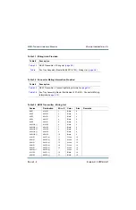
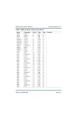
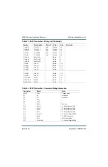
This section contains electrical schematics and logic diagrams for the transmitter. Block 

diagrams, simplified electrical schematics, and logic diagrams may be included. Refer to 

Table 4.1 on page 4-5

 for an itemized listing.

Component values

Unless otherwise specified on the logic or schematic diagram, the following defaults apply:

• Resistor values are shown in ohms (K = 1,000 and M = 1,000,000)

• Resistor power ratings are not shown when less than 0.5 W

• Capacitor values are shown in microfarads (uF)

• Unidentified diodes are part number 1N4938 (Nautel Part # QAP29)

Graphic symbols

The graphic symbols used on electrical schematics are in accordance with 

American National 

Standard ANSI Y32.2-1975 - Graphic Symbols for Electrical and Electronic Diagrams

.

Logic symbols

The logic symbols used on electrical schematics and logic diagrams are in accordance with 

American National Standard ANSI Y32.14-1975 - Graphic Symbols for Logic Diagrams

.

Reference designations

Referenced designations were assigned in accordance with 

American Society of Mechanical 

Engineers ASME Y14.44-2008 - Reference Designations for Electrical and Electronic Parts and 

Equipment

Each electrical symbol is identified with its basic reference designation. To obtain the full 

reference designation for a specific part, prefix this basic identifier with the reference 

designation assigned to all higher assemblies. For example, the complete designation for a 

resistor (

R1

) on a printed wiring board (

A1

), that is part of a larger board (

A2

), would be 

A2A1R1

.

Summary of Contents for NX50

Page 1: ...NX50 Transmitter Troubleshooting Manual Document NHB NX50 TRB Issue 6 0 2019 04 01 Status Standard...

Page 2: ......

Page 3: ...Fax 1 207 947 3693 Customer Service 24 hour support 1 877 628 8353 Canada USA only 1 902 823 5100 International Email support nautel com Web www nautel com The comparisons and other information provi...

Page 4: ......

Page 5: ...rface PWB replacement 1 66 Digital AM exciter PWB replacement 1 66 GPS Sync PWB replacement 1 71 USB Audio Interface PWB replacement 1 71 Exgine PWB replacement 1 72 PDM Drive Distribution PWB replace...

Page 6: ...s 2 4 Wiring connector lists 3 1 Wiring lists provided 3 1 Wiring lists not provided 3 1 Connector mating information 3 1 Wire colours 3 1 Printed wiring board patterns 3 1 Reading Electrical Schemati...

Page 7: ...NX50 Troubleshooting Manual Issue 6 0 2019 04 01 Page vii Mechanical Drawings 5 1 Identifying mechanical drawings 5 1 Content of mechanical drawings 5 1 List of terms 6 1...

Page 8: ...NX50 Troubleshooting Manual Page viii Issue 6 0 2019 04 01...

Page 9: ...NX50 Troubleshooting Manual Issue 6 0 2019 04 01 Page ix Release control record Issue Date Reason 6 0 2019 04 01 Supports release 6 of hardware NARA53E and software version NX SW 4 7 or higher...

Page 10: ...NX50 Troubleshooting Manual Page x Issue 6 0 2019 04 01...

Page 11: ...rocedures consist of identifying and correcting defects or deficiencies that arise during transmitter operation Local and or remote alarm signals are generated when a malfunction occurs If an alarm co...

Page 12: ...rs Analysis of this data will normally identify the type of fault and in most cases will determine what corrective action must be taken Refer to Identifying an alarm on page 1 5 to determine the remed...

Page 13: ...mbly from the transmitter and while handling the assembly for maintenance procedures Handling Storage An assembly should be placed in an anti static bag when it is not installed in a host transmitter...

Page 14: ...ution should be taken to ensure the static sensitive semiconductor devices are protected from unnecessary stress current This is achieved by ensuring that current is not flowing when an electrical con...

Page 15: ...bleshooting an alarm on page 1 7 The colour of the Status button at the bottom of the AUI indicates the severity of the highest offending alarm The button can display green amber or red When the Statu...

Page 16: ...b system apply to an exciter A or B Rack All Alarms in this sub system apply to a rack cabinet Rack 1 Module All Alarms in this sub system apply to a specific RF power module 1 through 20 Exgine For s...

Page 17: ...any troubleshooting record all AUI meter readings and note if any other alarms are displayed on the Transmitter Status page Record all alarms The most convenient way to do this is by using a web brow...

Page 18: ...the Operations Maintenance Manual for a description of the cutback routine Visually inspect the inside of the transmitter to locate the fault causing the arc detector to trigger Controller Brownout Re...

Page 19: ...e following settings from EEPROM upon boot up The transmitter will revert to its initial default settings which may be different from the values set before the transmitter was shipped The alarm will r...

Page 20: ...tter If the alarm persists replace the battery on the control interface PWB and retry the above steps If the alarm persists replace the control interface PWB see Control interface PWB replacement on p...

Page 21: ...e control interface PWB see Control interface PWB replacement on page 1 64 Controller Exciter Changeover This alarm indicates that an automatic exciter changeover has occurred This alarm will occur as...

Page 22: ...troller s reset pin If this alarm continues to occur unexpectedly replace the control interface PWB see Control interface PWB replacement on page 1 64 Controller Fast SWR Shutback This alarm indicates...

Page 23: ...curs when the GPS receiver is not responding to serial commands on the GPS sync PWB When this occurs the GPS sync PWB s phase lock loop will not be locked and the timing signals will be free running C...

Page 24: ...ect port on the transmitter Controller Host Not Booted This alarm indicates that the controller has not received any communication from the host since the last time the controller booted i e was power...

Page 25: ...lock is open and it will be necessary to locate the external device that is causing this condition If the impedance does not measure open circuit verify the interlock circuitry has been properly confi...

Page 26: ...that the PDM latch circuitry on the control interface PWB has tripped causing the transmitter to shut down and latch off If automatic changeovers are enabled and the transmitter is operating on the m...

Page 27: ...no AES data detected on the applicable AES 1 or 2 input and that same input is selected as the active input in either Analog or Digital settings for the active preset Verify there is valid AES data be...

Page 28: ...B sample has never been calibrated This alarm should only occur when replacing an exciter and indicates the configuration file was not properly uploaded see Digital AM exciter PWB replacement on page...

Page 29: ...replace the associated digital AM exciter PWB see Digital AM exciter PWB replacement on page 1 66 Exciter A B Entered Firmware Upgrade This alarm indicates that the exciter firmware is being upgraded...

Page 30: ...eing drawn from the B power supply as measured by the transmitter controller s Total B Current meter exceeded 245A The alarm will clear once the transmitter s forward power is no longer being reduced...

Page 31: ...Exciter A B Low B Voltage This alarm occurs when the B voltage measured by the exciter drops below 75 of the B setpoint for more than 10 seconds When this alarm is present the exciter will not allow t...

Page 32: ...layed for information only If the transmitter s Sync Source is set to GPS Sync Card check the connection between the GPS sync PWB and the control interface PWB If the connection is OK replace the GPS...

Page 33: ...hout the presence of the Controller s Fast SWR Shutback alarm verify the RF current sample RF voltage sample and the wiring between the sample point and the control interface PWB is not damaged If the...

Page 34: ...The exciter should automatically reboot itself however if the alarm persists press the reset button on the associated digital AM exciter PWB If the alarm persists replace the associated digital AM ex...

Page 35: ...y resetting transmitter alarms to clear power module faults If the alarm persists repair or replace RF power modules to clear this alarm see RF power module troubleshooting on page 1 47 Exciter A B Tr...

Page 36: ...XO value with the new DAC value as reported from the Exgine status screen Set the limits back to 0 95 ppm Restart the system and ensure the alarm is cleared Exgine Lost External 10MHz This alarm is oc...

Page 37: ...Removing and reinstalling RF power modules on page 1 51 Module External Disable Active This alarm indicates the PDM cable has been disconnected from the front of the RF power module which causes the...

Page 38: ...ciated RF power module to disable itself This alarm generally indicates that a modulator FET has failed See Troubleshooting RF power modules on page 1 56 to determine whether to replace the affected R...

Page 39: ...e 1 48 Module Low Fan 1 or 2 Speed This alarm occurs if the RF power module is expected to produce RF power and the fan 1 or 2 tachometer drops below 1650 RPM The affected RF power module is immediate...

Page 40: ...the RF power module see Removing and reinstalling RF power modules on page 1 51 If the alarm remains with the position replace the rack interface PWB see Rack Interface PWB replacement on page 1 76 Mo...

Page 41: ...shut down when this condition exists and prevent the transmitter from generating RF In a safe manner measure the voltage of each phase of the ac mains If a phase is missing check the ac mains fuses I...

Page 42: ...eding the shutback limit If it is not exceeding the limit verify the ac mains transformer is tapped correctly see Installing the power transformer on page 3 1 in the Installation Manual Rack High B Vo...

Page 43: ...ed correctly see Installing the power transformer on page 3 1 in the Installation Manual If so monitor the ac mains for transient conditions when this alarm occurs See Rack Low AC Voltage on page 1 49...

Page 44: ...terface PWB replacement on page 1 76 Rack 15 V A or B Fail The digital fault reporting output of either 15 V power supply U3 or U4 is active If the overall 15 V Fail alarm is active follow the trouble...

Page 45: ...B replacement on page 1 76 Rack 48 V A or B Fail If the overall 48 V Fail alarm is active follow the troubleshooting steps for that alarm Otherwise check continuity of the cabling between the associat...

Page 46: ...ter Fault Summary Exciter Summary This summary alarm is triggered if any of the following Exciter related alarms occur Controller alarms Audio Loss Shutdown High RF Drive Exciter Changeover Low RF Dri...

Page 47: ...r alarms GPS Not Responding GPS Receiver Not Responding GPS Unlocked GPS PLL Unlocked GPS Sync No 1 PPS High Reflected Power Summary Refl Power Summary This summary alarm is triggered if any of the fo...

Page 48: ...Voltage No External 10MHz External Inhibit Active No B Sample Precorrection Inhibited Exgine alarms AM FM Mode Mismatched FIFO Underflow Network Misconfigured DPLL Unlocked Lost External 10MHz System...

Page 49: ...ary alarm is triggered if any of the following output network related alarms occur Controller alarms Arc Shutback Fast SWR Shutback Exciter alarms Cutback Over Current Shutback SWR Shutback High Forwa...

Page 50: ...5V Fail 15V Fail High Rectifier Temp 15V A B Fail 15V A B Fail Low AC Voltage Rack Fault Summary Rack Summary This summary alarm is triggered if any of the following rack related alarms occur Controll...

Page 51: ...6 GPS Sync PWB See page 1 71 USB Audio Interface PWB See page 1 71 Exgine PWB See page 1 72 PDM Distribution PWB See page 1 73 RF Drive Distribution PWB See page 1 74 Rack Interface PWB See page 1 76...

Page 52: ...ol Exciter panel allows access to the Directional Coupler assembly A43 Rear Access The rear of the NX50 has a lockable hinged door for safety purposes Opening the door allows access to the power trans...

Page 53: ...ternal power supply using user provided shorting jumpers on terminal block TB1 see External PDM inhibit on page 8 3 of the Pre Installation Manual 1 Gain access to the control exciter panel A11 see Fi...

Page 54: ...see External system interlock on page 8 2 of the Pre Installation Manual 1 Gain access to the control exciter panel A11 see Figure 1 9 on page 1 65 by opening the control cabinet s front door 2 Conne...

Page 55: ...mal press the Status button on the AUI to check for other alarms that may have triggered the RF power module alarm 3 From the AUI s Meter List View page see Figure 1 2 click the i information button n...

Page 56: ...NX50 Troubleshooting Manual Responding to alarms Page 1 46 Issue 6 0 2019 04 01 Figure 1 3 RF Module Status Screen all modules Figure 1 4 RF Module Status Screen individual module...

Page 57: ...long red short off module has no valid serial number short red long off module has no valid serial address on the internal bus long amber short green module is producing RF but is receiving no serial...

Page 58: ...RF power modules and therefore has four B fuses F1 through F4 Refer to Figures MD 1 and MD 2 in the Mechanical Drawings section of this manual to locate the associated power module interface PWB and t...

Page 59: ...0 Installation Manual If necessary turn off the transmitter lock out the ac input voltage and retap the power transformer for the next lower voltage 4 If the transformer taps are correct the rectifier...

Page 60: ...pped as shown in Section 3 Installing the power transformer on page 3 1 of the NX50 Installation Manual If necessary turn off the transmitter lock out the ac input voltage and retap the power transfor...

Page 61: ...r module is disabled 3 When the RF power module is disabled you should hear a relay in the back of the cabinet drop out de energize Proceed to Step 4 if you hear the relay click If you do not hear the...

Page 62: ...nsmitter Figure 1 5 Disabling Enabling an RF Power Module NOTE To maintain proper airflow in the transmitter install the dummy module assembly Nautel part 207 1038 located in the NX50 ancillary kit if...

Page 63: ...ble RJ45 connector to the front of the RF power module 5 If the RF power module was disabled through the AUI enable it as follows From the Meters page click on the Modules Rack information i button Th...

Page 64: ...NX50 Troubleshooting Manual Responding to alarms Page 1 54 Issue 6 0 2019 04 01 Figure 1 6 RF Power Module Locations RF Power Modules Front Door Removed for Clarity...

Page 65: ...f and connect the RF output to a suitably rated 50 ohm test load 2 Using the AUI set the following items as instructed Overall Mode Analog AM Output Power rated power AM Source Unused 3 Set the transm...

Page 66: ...e A soldering iron and desoldering tool An NX50 spares kit contains replacement semi conductors Electrostatic Precautions The RF power module contains semiconductor devices that are susceptible to dam...

Page 67: ...w head terminals and Q11 through Q13 have solder pads see Figure 1 7 on page 1 59 Check for 1 000 between the gate and source Check for an open circuit between the gate and drain 3 If either measureme...

Page 68: ...e 1 7 on page 1 59 to identify the free wheel diodes on the RF power module 1 Use a digital multimeter on its diode setting to check free wheel diodes CR19 through CR21 noting the anode A and cathode...

Page 69: ...and Diode Location G D S G D S G D S Q13 Q12 Q11 Modulator MOSFETs Q11 Q12 and Q13 A CR9 K Protection diode CR9 A CR21 K CR20 A K A CR19 K Free wheel diodes CR19 CR20 and CR21 Some parts removed for c...

Page 70: ...4 Discard the defective MOSFET and its associated thermal pad between MOSFET and heatsink 5 Ensure the surface of the heatsink is clean and free of debris 6 Obtain a replacement MOSFET Nautel Part QR...

Page 71: ...NX50 Troubleshooting Manual Responding to alarms Issue 6 0 2019 04 01 Page 1 61 Figure 1 8 Power Amplifier FET Replacement...

Page 72: ...re the defective device s heatsink to the PWB Remove the heat sink and the device from the PWB 5 Remove the heatsink clip that holds the device on its heat sink Remove and discard the defective device...

Page 73: ...r the anode A and cathode K connections 10 Replace any other defective devices and then reinstall the PWB to the chassis by reversing the instructions in steps 1 2 and 3 Torque the 16 power amplifier...

Page 74: ...ctor labels on the cables and the PWB 4 Remove and retain the two screws securing the connector bracket in the upper right portion of the control interface PWB 5 Remove either the remote interface PWB...

Page 75: ...ngs Time Setup page 13 Measure the VSWR threshold voltage on the control interface PWB at R73 LHS Adjust VSWR THRESHOLD potentiometer R78 until the multimeter reading is 1 5 Vdc 14 Set the transmitter...

Page 76: ...nector loose with a screwdriver 6 Set the STATUS ALARM jumpers E1 through E16 on the new remote interface PWB to the same positions as the defective PWB 7 Use an indelible marker to identify the LED a...

Page 77: ...FTP site ftp www3 nautel com Utilities NCodeUploader 5 From the PC run the NCode Uploader version 1 8 or higher application see Figure 1 11 on page 1 67 Click Settings and ensure the COM port reflect...

Page 78: ...lick the Read Exciter Configuration button Select Save file to disk and click OK see Figure 1 13 to save the current calibration data Browse to a desired location to save the file 8 If the defective e...

Page 79: ...trol interface PWB A11A1 It may be helpful to gently pry the connectors loose with a screwdriver keeping to the far left or right edge of the connector alternating between connectors to avoid damage 1...

Page 80: ...file field see Figure 1 14 Figure 1 14 Upload DSP Firmware Menu Browse for configuration file 18 Click the Program Exciter Configuration checkbox see Figure 1 14 on page 1 70 so that the box contains...

Page 81: ...4 sets of mounting hardware from the GPS sync PWB from the exciter panel 4 Obtain a replacement GPS sync PWB Nautel Part NAPX46 Remove the jack screws from 9 pin D sub connector J1 on the new GPS sync...

Page 82: ...e Settings and record all fields with exception of the MAC Address 2 Set the transmitter to its RF Off state Turn off disable the ac power at the source Open the front door to gain access to the excit...

Page 83: ...on the cables and the PWB 3 Remove and retain six 6 sets of mounting hardware 4 Remove the defective PWB from the transmitter 5 Obtain a replacement PDM Drive Distribution PWB Nautel Part NAPI154 6 R...

Page 84: ...tion and Rack Interface PWBs WARNING Lethal voltages exist inside the transmitter when the power is turned on Turn off disable and lock out the power at the source and verify no dangerous ac or dc vol...

Page 85: ...ages at the ac input terminals There should be little or no ac or dc voltage DO NOT PROCEED if either the ac or dc voltage is greater than 5V 2 Carefully remove and retain the six 6 M3 screws used to...

Page 86: ...e across the and terminals of any of the large electrolytic capacitors on the floor of the cabinet as well as the line to line and line to ground voltages at the ac input terminals There should be lit...

Page 87: ...bles in Section 3 Wiring connector lists on page 3 1 9 Disengage all RF power modules in the transmitter before turning on the ac power see Removing and reinstalling RF power modules on page 1 51 10 C...

Page 88: ...ged For additional safety measure the dc voltage across the and terminals of any of the large electrolytic capacitors on the floor of the cabinet There should be little or no voltage WARNING Lethal vo...

Page 89: ...e SCR rectifier assembly from the transmitter 6 Obtain a replacement SCR rectifier assembly Nautel Part 207 7055 05 7 Reverse Step 3 through Step 5 to reinstall the new or repaired SCR rectifier assem...

Page 90: ...ter than 5V 2 Inspect the SCR rectifier assembly s cooling fans see Figure 1 18 on page 1 78 for debris that might restrict proper movement of the fan blades Try spinning the fan blades to loosen or f...

Page 91: ...or additional safety measure the dc voltage across the and terminals of any of the large electrolytic capacitors on the floor of the cabinet as well as the line to line and line to ground voltages at...

Page 92: ...bracket to the side skin of the transmitter 4 Remove the power supply module from the transmitter noting its reference designation U3 through U7 should be marked on the side panel near the module 5 Re...

Page 93: ...ule Reconnect all wiring and ensure all connections are tight noting there are special torque requirements for the L N G V and V terminals for each supply U3 and U4 require 60 in lb 6 78 Nm for V and...

Page 94: ...of mounting hardware Pull the fan tray assembly out of the transmitter 5 Obtain a replacement fan tray Nautel Part 207 8133 6 Reverse Step 1 through Step 4 to install the new fan tray assembly Ensure...

Page 95: ...wo 2 M4 screws that secure the fan to the tray 4 Obtain a replacement fan Nautel Part ZAP37 from the site spares kit if purchased vendor part is Sanyo Denki America Inc 109E5748C503 5 Reverse Step 2 a...

Page 96: ...lying the Single Board Computer Failure to do this step could result in hardware damage 3 Disconnect the three 3 cables connected to the LCD touchscreen monitor i e 12 V power VGA and Serial COM 4 Rem...

Page 97: ...ree targets from a position of normal use Touch each target After the third target the calibration is complete and the screen display returns to the Screen Configuration page The replacement procedure...

Page 98: ...lacement SBC Nautel Part 207 8710 01 Obtain the flash card see Figure 1 23 on page 1 87 from the SBC removed in Step 5 and insert it into the replacement SBC If a new flash card is used note that many...

Page 99: ...talled software versions and the selected software upgrade file should appear 9 In the Software Versions screen see Figure 1 24 if there are any red highlighted lines compare the Installed Version col...

Page 100: ...ion of Arc Detector Assembly WARNING Lethal voltages exist inside the transmitter when the power is turned on Turn off disable and lock out the power at the source and verify no dangerous ac or dc vol...

Page 101: ...he cable and the assembly 3 Carefully remove and retain the two 2 sets of mounting hardware and remove the arc detector assembly from the transmitter chassis Remove the UV sensor U2 from the arc detec...

Page 102: ...ge 1 92 Issue 6 0 2019 04 01 Figure 1 26 Arc Detector Assemble UV Photo Tube Sensor UB89 Figure 1 27 UB89 Orientation on Driver PWB U1 Assembly may not be exactly as shown Anode Lead Cathode Lead Conn...

Page 103: ...ation of RF Voltage Probe WARNING Lethal voltages exist inside the transmitter when the power is turned on Turn off disable and lock out the power at the source and verify no dangerous ac or dc voltag...

Page 104: ...floor of the cabinet as well as the line to line and line to ground voltages at the ac input terminals There should be little or no ac or dc voltage DO NOT PROCEED if either the ac or dc voltage is gr...

Page 105: ...n of RF Current Probe WARNING Lethal voltages exist inside the transmitter when the power is turned on Turn off disable and lock out the power at the source and verify no dangerous ac or dc voltages a...

Page 106: ...re 1 29 on page 1 95 for the location of the RF Current Probe A42 3 Remove the left hand side panel viewed from the front of the transmitter by removing and retaining the three M5 screws on the top of...

Page 107: ...Troubleshooting Manual Responding to alarms Issue 6 0 2019 04 01 Page 1 97 Figure 1 30 Location of Mounting Hardware M12 BOLT Partial View Rear Door and LHS panel removed for clarity M8 BOLTS Quantit...

Page 108: ...NX50 Troubleshooting Manual Responding to alarms Page 1 98 Issue 6 0 2019 04 01...

Page 109: ...P39C assigned to the assembly containing the part or the full reference designation including the reference designation of all higher assemblies must be known When the nautel nomenclature is known Ref...

Page 110: ...el Stock Code Column This column contains the Component Level number 01 through 10 as required and the Nautel Stock Code part number assigned to each part Component Level This number represents the le...

Page 111: ...ludes Nautel part numbers only It does not include original equipment manufacturer OEM information i e vendor part numbers Some vendor information is provided in the Responding to Alarms section of th...

Page 112: ...ations acronyms may appear in the Description of Part column SMT Denotes item is designed to be installed using Surface Mount Technology MTA Denotes item is a Mass Termination Assembly connector SIP S...

Page 113: ...B AUDIO INTERFACE PWB OPTIONAL NAPI151 CURRENT PROBE A42 207 6213 10 RF DRIVE DISTRIBUTION PWB NAPI98 A7 A11A4 REMOTE INTERFACE PWB NAPI106 B DISTRIBUTION ASSEMBLY A9 NAX243B 01 SAME AS A15 A16 A34 RF...

Page 114: ...HOKE A44 183 6059 A47U2 UV PHOTO TUBE SENSOR UB89 UG53 U3 15V POWER SUPPLY CAPACITOR ASSEMBLY A46 207 7120 04 A48U1 SCR 3 PH RECTIFIER UR92 UG54 U5 48V POWER SUPPLY A48 25 50 kW RECTIFIER ASSEMBLY 207...

Page 115: ...sistor Film 100 Ohms 5 2W R03 R04 RBP36 02 Resistor Film 39 Ohms 5 2W R01 UC89 02 Transducer Current 0 1V A 150Arms max Isolated T01 207 7055 05 01 15 25 50KW Rectifier Assy A48 207 7144 02 02 AC Powe...

Page 116: ...JR39 02 Conn Plug D Sub 25 pin HDP 20 P06 P07 P08 JT116 02 Conn Mate N Lok Plug 2 600V 36A 250 Centerl P35 JT16 02 Conn Lock Screw D Sub Male Kit P01 P02 P03 P04 P05 P06 P07 P08 P09 P10 P11 P14 P15 P...

Page 117: ...y Module Assy Nx Series 207 8428 02 AC Entry Adapter Plate Asy for WG53 207 8517 01 01 Cableform AC Rect O P Stn GND NX50 RLS 4 215 8065 01 Arc Detector Shielded Assy A47 CCF06 02 Capacitor Tantalum E...

Page 118: ...C143 C144 C146 C148 C151 C152 C157 C158 C160 C162 C163 C164 C167 C168 C169 C171 C172 C173 C176 C178 C180 C181 C182 C186 C187 C191 C192 C195 C197 C199 C200 C204 C205 C206 C207 C208 C211 C215 C218 C219...

Page 119: ...CR10 CR11 CR12 CR20 CR32 CR33 CR34 CR35 CR36 CR37 CR38 CR42 CR43 CR44 CR45 CR47 CR49 CR51 CR53 CR55 CR57 CR61 CR62 CR63 CR64 CR65 CR66 CR67 CR68 CR69 CR70 CR71 CR72 CR73 CR74 CR75 CR76 QDSS01 03 Diode...

Page 120: ...R256 R361 RFFS27 03 Resistor SMT MF 121ohms 1 1 10W 0603 R134 R147 R174 RFFS30 03 Resistor SMT MF 221ohms 1 1 10W 0603 R071 RFFS31 03 Resistor SMT MF 274ohms 1 1 10W 0603 R211 RFFS34 03 Resistor SMT...

Page 121: ...T MF 1 00Mohms 1 1 10W 0603 R035 R038 R041 R056 R057 R058 R059 R065 R067 RT16 03 Thermistor PTC 50 77 Ohms 0 5A Hold RT03 RT17 03 Thermistor PTC 15 25 Ohms 1 1A Hold RT01 RT02 RT04 RT20 03 Resistor SM...

Page 122: ...ual SO 8 U55 UT110 03 IC Voltage Regulator 1 5A ADJ Low Drop U34 UT70 03 IC SMT High Speed Comparator SOIC 8 U13 U31 U37 UT73 03 IC DC DC Converter 3kV ISO 5V 5V 1W U08 UT79 03 IC Variable Gain Amp SM...

Page 123: ...C131 C132 C133 C134 C135 C136 C137 C138 C139 C141 C142 C143 C144 C145 C146 C147 C148 C149 C150 C152 C153 C154 C155 C156 C157 C158 C159 C160 C161 C162 C163 C164 C165 C166 C167 C168 C169 C170 C171 C172...

Page 124: ...FFS38 03 Resistor SMT MF 1000ohms 1 1 10W 0603 R02 R26 R45 R74 R76 RFFS39 03 Resistor SMT MF 1210ohms 1 1 10W 0603 R72 RFFS40 03 Resistor SMT MF 1500ohms 1 1 10W 0603 R73 RFFS42 03 Resistor SMT MF 221...

Page 125: ...Temp U27 UX64 03 IC SMT Power Supervisor Dual I P 33 1 5V MSOP U22 UX65 03 IC SMT 3A Sync Buck Converter SO 20 w pwr pad U14 UX66 03 IC SMT Linear Regulator 150mA Adj MSOP 8 U10 UX67 03 IC SMT Linear...

Page 126: ...n PW B Mt J03 JS21 03 Conn BNC Recept Rt Angle P WB Mt J01 J02 LA16 03 Inductor Choke 2 5 Turns J Mtl L01 L02 RAB22 03 Resistor MF 562 Ohms 1PC 1 4W R14 RAB27 03 Resistor MF 1 50K Ohms 1PC 1 4W R13 R1...

Page 127: ...Elect 1000uF 50V C05 FA34 03 Fuse 20A 500Vdc Non Time De lay KLM F01 F02 F03 F04 FC27 03 Fuse Clip 20A 13 32 Dia Fuse PWBMt XF01 XF02 XF03 XF04 HAC55 03 Terminal PC Screw 10 32 30 Amp E01 E02 E03 E04...

Page 128: ...or SMT 0 054u NPO 5 J lead 4x2225 1 C116 C117 CTFS03 03 Cap SMT Tantalum 10uF 10 35V 2917 C005 C016 C021 C025 C144 C145 C146 C147 FA46 03 Fuse SMT Fuse Block 3A Very Fast Acting Installed F01 JF47 03...

Page 129: ...Resistor SMT MF 3320ohms 1 1 10W 0603 R048 R049 R050 R060 R086 RFFS49 03 Resistor SMT MF 8250ohms 1 1 10W 0603 R082 RFFS50 03 Resistor SMT MF 10 0Kohms 1 1 10W 0603 R007 R008 R009 R028 R032 R033 R034...

Page 130: ...C184 CCFS23 02 Cap SMT Ceramic 18pF 2 50V C0G 0603 C013 C018 CCFS52 02 Cap SMT Ceramic 0 1uF 10 25V X7R 0603 C001 C005 C009 C011 C014 C015 C017 C023 C025 C026 C027 C028 C029 C030 C031 C032 C033 C038...

Page 131: ...3 Q01 QR28 02 Thyristor SCR 65A 400V Q02 Q03 RAD17 02 Resistor SMT MF 221 Ohms 1 1 4W R044 R045 RAD25 02 Resistor SMT MF 1000 Ohms 1 1 4W R065 R084 R093 RAD39 02 Resistor SMT MF 15K Ohms 1 1 4W R005 R...

Page 132: ...R024 R034 R056 R060 R107 R133 RFFS54 02 Resistor SMT MF 22 1Kohms 1 1 10W 0603 R009 R013 R108 R150 R174 R175 R177 R178 RFFS57 02 Resistor SMT MF 39 2Kohms 1 1 10W 0603 R008 RFFS58 02 Resistor SMT MF...

Page 133: ...z Y01 NAPI154 01 PDM Drive Distribution PWB A08 CCFS07 02 Cap SMT Ceramic 0 1uF 10 50V X7R 0805 C001 C002 C003 C004 C005 C006 C007 C008 C013 C015 C019 C020 C022 C024 C026 C028 C030 C032 C034 C036 C038...

Page 134: ...80 C081 C082 C083 C084 C097 C098 C100 C102 CCFS10 02 Cap SMT Ceramic 1uF 10 25V X7R 1206 C013 C014 C015 C016 C017 C018 C019 C020 C021 C022 C023 C024 C037 C038 C039 C040 C041 C042 C043 C044 C045 C046 C...

Page 135: ...46 02 Resistor Film 470K Ohms 0 1 1W R01 R02 RC44 01 Resistor Cap Discharge 27Komhs 5 13W A46R1 A46R2 A46R3 A46R4 A46R5 A46R6 TF44B 01 Inductor Choke 8mH 60A L01 L02 L03 L04 UB89 01 Sensor Flame UV ph...

Page 136: ...anual for detailed wiring information for these assemblies if provided Assemblies that have their wiring information shown in tables on their assembly detail drawing s Refer to the Mechanical Drawings...

Page 137: ...ay Assembly Nautel Part Number 207 8133 Connector Mating Information page 3 12 Table 3 3 NX50 Transmitter Wiring List Source Destination Wire Color Size Remarks A9E1 A1A1E1 1 Black 6 A9E2 A2A1E1 2 Bla...

Page 138: ...e 22 P01 04 P06 02 104 White 22 P01 05 GND near A39 105 Black 22 P01 06 P07 11 106 White 22 P02 01 P06 04 107 White 22 P02 02 GND near A39 108 Black 22 P02 03 P07 23 109 White 22 P02 04 P06 05 110 Whi...

Page 139: ...r shielded P08 23 P14 23 Shield P08 12 P14 12 141A White 22 2 Conductor shielded P08 24 P14 24 141B Black 22 P08 25 P14 25 141 Shield P08 14 P14 14 143 Black 22 P08 15 P14 15 144 White 20 P08 16 P14 1...

Page 140: ...ack 20 P11 02 U5 V 172 Black 20 P11 03 U5 V 173 White 20 P11 06 P26 03 174 White 22 P11 07 P22 02 175 White 22 P11 08 P19 02 176 White 22 P11 09 P25 04 177 White 22 P11 10 P26 04 178 White 22 P11 11 A...

Page 141: ...L E4 T1XF1 4 203 White 14 XF1 4 LINE Fuse R U3 L T1XF1 2 204 White 14 U3 N T1XF1 4 205 White 14 U3 G GND near U3 206 Black 14 U3 L U4 L 207 White 14 U3 N U4 N 208 White 14 U3 G U4 G 209 Black 14 U6 L...

Page 142: ...U3 238 Black 8 A44 B GND near A44 239 Yellow 14 A44 A RF OUT STUD 240 Yellow 14 A43C1 Top RF OUT STUD 241 Yellow 14 T1 GND GND near L4 242 Grn Yel 6 U8E1 E5 243 Yellow 18 L1 1 A48U1 B 300 Black 2 L1...

Page 143: ...ine 3 2 Black 1 0 T1 LINE3 Line 3 2 Black 1 0 Fr Door GND GND 1 Braid 14 Rr Door GND GND 2 Braid 14 Ex Door GND GND 3 Braid 14 Table 3 4 NX50 Transmitter Connector Mating Information Connector Mate No...

Page 144: ...o Front Door Computer P33 A65A1U1F_PANEL1 To Front Door Computer P35 A48A1J1 AC Power Indicator P4 A38J1 Fan Tray P5 A39J1 Fan Tray P6 A6J8 To Rack Interface PWB P7 A6J9 To Rack Interface PWB P8 A6J11...

Page 145: ...J3B W23P2 A2A1J11 W24P1 A7J2H W24P2 A2A1J12 W25P1 A7J2F W25P2 A3A1J11 W26P1 A7J2D W26P2 A3A1J12 W27P1 A7J2B W27P2 A4A1J11 W28P1 A7J1H W28P2 A4A1J12 W29P1 A7J1F W29P2 A5A1J11 W2P1 A25A1J1 W2P2 A8J1C W3...

Page 146: ...0A1U1COM1 Serial Bus W69P1 A6J1 W69P2 A1A1J6 W6P1 A27A1J1 W6P2 A8J3C W70P1 A6J5 Add Labels to W70 W70P2 A5A1J6 W7P1 A18A1J1 W7P2 A8J4B W8P1 A28A1J1 W8P2 A8J4C W9P1 A19A1J1 W9P2 A8J5B Table 3 5 Fan Tra...

Page 147: ...nector Mating Information Connector Mate Note B1E1 E1 Fan 1 Red Wire V B1E2 E2 Fan 1 Black Wire V B1E3 E3 Fan 1 Yellow Wire TACH B2E1 E4 Fan 2 Red Wire V B2E2 E5 Fan 2 Black Wire V B2E3 E6 Fan 2 Yello...

Page 148: ...ls used on electrical schematics are in accordance with American National Standard ANSI Y32 2 1975 Graphic Symbols for Electrical and Electronic Diagrams Logic symbols The logic symbols used on electr...

Page 149: ...active true state of the signal The high suffix indicates the more positive of the two levels used to represent the logic states The low suffix indicates the less positive of the two levels Two types...

Page 150: ...a reference designation e g A2A1 refer to the family trees in Section 2 Parts Lists on page 2 1 Follow the family tree branches to the block that contains the desired reference designation and associa...

Page 151: ...ach family tree block in the path starting at the highest assembly this is normally Figure MD 1 to determine the figure number s for that assembly Example NAPA34A Modulator Power Amplifier PWB is show...

Page 152: ...Sheet 4 of 7 SD 11 NAPC160C 01 Control Interface PWB Sheet 5 of 7 SD 12 NAPC160C 01 Control Interface PWB Sheet 6 of 7 SD 13 NAPC160C 01 Control Interface PWB Sheet 7 of 7 SD 14 NAPI106 Remote Interf...

Page 153: ...NX50 Troubleshooting Manual Reading Electrical Schematics Page 4 6 Issue 6 0 2019 04 01...

Page 154: ...ETURN 2 B RETURN 1 CAPACITOR 13W 450V 10 000 C5 C4 B 5 B 4 B 3 B 2 B 1 GBPC3508 CONTROL STAGE STAGE RF POWER GND AC COM 3 AC 3 J1 P35 2 A DS2 A DS3 N SUPPLY V 12V POWER G A47 ASSY L N V 480W 48V POWER...

Page 155: ...J20 5 2 J8 P40 A11A1 CONTROL J2 18 13 17 20 9 19 5 AM EXCITER J19 3 A11A3 10 J2 8 13 9 19 12 10 3 J17 6 A11A2 2 10 8 GND GND GND PDM 9 EXCITER B PDM 4 EXCITER B GND GND GND DUMP 2 EXCITER A PDM 9 EXC...

Page 156: ...PUT 16 DIGITAL INPUT 12 N C DIGITAL INPUT 08 GND DIGITAL INPUT 03 AC DC POWER GPS PWB J1 INTERLOCK INHIBIT 15V 15V ANALOG J2 REMOTE INTERFACE PART 1 OF 2 ADDRESS GPS 10 MHz GPS INTERNAL BUS INTERFACE...

Page 157: ...RN 15V RETURN 11 22 15V RETURN 20 10 8 4 FAN TACH F FAN TACH R 6 A5A1J6 MODULE BUS 10KW POWER RF DR 1 RF DR 2 RF DR 1 RF DR 2 RF DR 1 RF DR 2 A5A1J12 RF DR 1 RF DR 2 RF DR 1 RF DR 1 A5A1J11 PDM CABLE...

Page 158: ...3 9100pF C4 9100pF C5 DRAIN A44 OPTIONAL STN GND KEY U8 1 0 C25 0 1 C24 10 C26 35V 0 5W 220 R12 0 1 C17 2 1 7 U1 A RF CURRENT PROBE PART OF A1 PART OF A2 SAME AS ABOVE PART OF A3 SAME AS ABOVE RF TRA...

Page 159: ...64 1 OF 4 61 59 56 54 51 P1 3 1N4004 CR2 1N4004 CR1 E3 E4 3 1N4004 CR3 P1 2 E5 E6 11 12 24 21 8 9 TRANSFORMER A24 A19 A5A3 PWB A4A1 A3A2 POWER B RETURN 7 8 3 DUMP PDM 3 PDM 1 100K 2W R3 470 450V C3 M...

Page 160: ...10 0K R82 10 0K R186 5V 5V 5V BT1 3V 10 0K R190 10 0K R192 10 0K R196 A10 A8 A11 A13 RD 5V 5V DS3 A DS2 A LS1 MSR516N 5V 5V 5V 5V 10 0K R185 10 0K R221 10 0K R252 6 SCL 8 VDD 5V DS6 A DS5 A RESET S7 4...

Page 161: ...10 0K R82 10 0K R186 5V 5V 5V BT1 3V 10 0K R190 10 0K R192 10 0K R196 A10 A8 A11 A13 RD 5V 5V DS3 A DS2 A LS1 MSR516N 5V 5V 5V 5V 10 0K R185 10 0K R221 10 0K R252 6 SCL 8 VDD 5V DS6 A DS5 A RESET S7 4...

Page 162: ...C 11 10 9 U17 C 11 10 9 U3 C 11 10 9 U2 C 11 10 9 U15 C 11 10 9 U5 C 5 6 7 U17 B 5 6 7 U3 B 5 6 7 U16 B 5 6 7 U14 B 5 6 7 U15 B 5 6 7 U5 B 3 2 1 U3 A 3 2 1 U16 A 3 2 1 U14 A 3 2 1 U4 A 3 2 1 U5 A R24...

Page 163: ...1 J19 22 J19 10 J17 C200 0 1 CS_DAC1 MOSI C191 0 1 L14 C198 1 0 10 0K R239 5V L16 7 CLK TLV5620ID U63 5 REFD 1 GND 3 REFB 2 REFA 4 REFC 6 DATA 13 LDAC 14 VDD 5V 5V C196 0 01 10 0K R230 10 0K R231 10 0...

Page 164: ...3 13 C 4750 R285 11 A 2 SO 15 CLK_INH 8 GND 0 1 C225 18 J24 16 J24 13 J24 11 J24 0 01 C232 CR61 10 0K R293 R313 4750 0 01 C234 CR63 10 0K R295 R315 4750 0 01 C236 CR65 10 0K R297 R316 4750 R318 4750 0...

Page 165: ...10 RESET 12 LATCH_CLK 4 QE 6 QG 2 QC 12 LATCH_CLK 7 QH 15 QA MC74HC595AD U72 10 RESET 5 QF 1 QB 3 QD 7 10 U84 G 4 13 U85 D 2 15 U85 B 15V 25 J19 B2 J3 13 J19 5V 24 J19 24 J17 12 J17 20 J23 R339 12 1...

Page 166: ...C135 49 9 R143 49 9 R144 0 01 C114 3 6 4 5 MOCD223 M U42 B 5V 49 9 R141 49 9 R142 49 9 R132 49 9 R133 0 1 C130 7 10 U47 G 5V 5V 8 7 3 2 U54 A R169 27 4K 1000 R178 DS36C278TM U40 9 10 11 U45 C C270 0 1...

Page 167: ...2 G DS1 B STATUS ALARM DS1 A R CR1 CR8 E8 2 STATUS E8 3 E8 1 G DS8 B E6 3 E6 1 1500 R6 15V 15V CR4 1500 R4 15V 15V G DS4 B E2 2 E2 1 STATUS G DS2 B E2 3 CR2 DIGITAL OUT 05 DIGITAL OUT 04 23 J1 24 J1...

Page 168: ...PS 3 3V 3 3V 0 1 C13 0 1 C17 TP4 5 I O GTS1 2 I O GTS2 27 F3M9 40 F3M12 42 F3M16 52 F4M12 29 TMS 53 TDO 25 F3M8 24 F3M5 14 GND 41 GND 63 F2M8 4 F2M12 20 F1M17 TP3 59 F2M4 34 F3M6 3 J4 JTAG 5 J4 R11 49...

Page 169: ...CK 5 DOUT 14 VOUTL 18pF C9 18pF C10 1 00M R8 Y1 12 000MHz 10 9 8 U2 C 4 5 6 U2 B 1 2 3 U2 A 13 12 11 U2 D 0 1 C11 R6 100 R7 100 221 R10 R4 100 R5 100 221 R9 4 J2 AES EBU 1 J2 AES EBU SHLD 3 J2 3 D 4 V...

Page 170: ...P50 29 PD4 IC1 5 PE3 OC3A AIN1 3 PE1 TXD0 PDO 20 RESET 5V R28 10 0K TP6 4750 R258 CS_ADDR R157 10 0K 63 GND 10 0K R100 10 0K R124 5V R38 274 0 1 C28 CE WR TP58 D0 D2 10 0K R26 D4 D6 TP64 TP62 TP70 5V...

Page 171: ...7 ADDRESS 15 CS 17 ADDRESS 0 1 C162 0 1 C163 0 1 C164 0 1 C166 7 A6 TLC1543IDW U21 0 1 C171 0 1 C169 8 A7 0 1 C168 0 1 C88 1 0 C87 0 01 C84 0 1 C78 BAT54HT1 CR5 5V BAT54HT1 CR8 0 01 C106 0 1 C102 0 1...

Page 172: ...BR1660 CR3 0 1 C172 R21 15 0K Q3 S4065K 9 10 8 U17 C 6 5 7 U17 B 0 1 C32 0 1 C33 1000 R59 1000 R32 R58 475K R33 475K 0 1 C59 0 1 C54 1000 R57 15 0K R56 R64 475K 0 1 C29 0 1 C25 10 0K R111 10 0K R30 R1...

Page 173: ...A 3 2 1 U18 A 5 6 7 U18 B 3 2 1 U6 A 3 2 1 U19 A 5 6 7 U19 B 3 2 1 U7 A 3 2 1 U20 A 5 6 7 U20 B 3 2 1 U8 A 5V 0 1 C83 0 1 C84 0 1 C72 10 GND 2 GND 20 VCC IDT74FCT807CTSO U30 1 IN 5 6 7 U21 B 3 2 1 U9...

Page 174: ...9 U20 C 13 14 15 U20 D 11 10 9 U8 C 5 O2 3 O1 13 GND 1 0 C93 6 GND 1 0 C57 IDT74FCT807CTSO U29 1 0 C94 4 VCC 8 VCC 1 IN 18 O9 16 O8 11 10 9 U9 C 14 O7 11 10 9 U21 C 13 14 15 U21 D 12 O6 11 10 9 U10 C...

Page 175: ...13 14 15 U29 D F8 J3 G1 J3 F5 J3 F6 J3 13 14 15 U26 D 11 10 9 U26 C E7 J3 E4 J3 F2 J3 13 14 15 U27 D 11 10 9 U27 C D5 J3 E3 J3 E1 J3 D8 J3 3 2 1 U27 A 13 14 15 U24 D D2 J3 C7 J3 D6 J3 13 14 15 U25 D...

Page 176: ...6C31TM U19 E 4 ENABLE 16 VCC 12 ENABLE 8 GND DS26C31TM U36 E 1 0 C43 4 ENABLE 16 VCC 12 ENABLE 8 GND DS26C31TM U17 E 4 ENABLE 16 VCC 12 ENABLE 8 GND DS26C31TM U34 E 1 0 C39 1 0 C41 4 ENABLE 16 VCC 12...

Page 177: ...H L10 0 15 C55 C113 1 0 C115 1 0 0 47 C134 4750 R125 0 47 C133 4750 R124 0 1 C78 CR9 STTH1212G 1000 R116 Q10 APT5010JLL Q9 APT5010JLL 57 P1 59 P1 62 P1 64 P1 52 P1 54 P1 37 P1 39 P1 42 P1 44 P1 34 P1...

Page 178: ...CR29 330 C129 25V 5V 5V R54 100K R74 100K 0 1 C26 1 0 C110 2 3 1 U21 A 5 6 7 U21 B R75 100K R95 10 0K CR10 1N4448HWS 1W R91 270 0 1 C69 R30 0 0 2 RE 1 RO L7 1000 R77 8250 R82 5V 12 13 14 U21 D 10 0K...

Page 179: ...ncluded where appropriate When a module or assembly is the subject of its own assembly detail drawing and it is also shown in a higher level assembly the detail depicted in the higher level assembly m...

Page 180: ...wer Module Interface PWB MD 5 NAE96C 01 Control Exciter Panel MD 6 NAPC160C 01 Control Interface PWB MD 7 NAPE78A 01 Digital AM Exciter PWB MD 8 NAPI106 Remote Interface PWB MD 9 NAPX46 GPS Sync PWB O...

Page 181: ...CITER PANEL A11 PDM DRIVE DISTRIBUTION ASSEMBLY A8 B DISTRIBUTION ASSEMBLY A9 RF OUTPUT U1 L1 FRONT DOOR A40 INNER OUTER SIDE PANELS and TOP REMOVED FOR CLARITY DIRECTIONAL COUPLER A43 RF POWER MODULE...

Page 182: ...C28 C29 C30 C17 C18 C19 C20 U3 U4 STATION REFERENCE GROUND T1 L1 A43 STATIC DRAIN CHOKE A44 L9 RACK INTERFACE PWB A6 RF DRIVE DISTRIBUTION PWB A7 are mounted on the underside of grill BACK PLANE RF C...

Page 183: ...Issue 6 0 2019 04 01 MD 3 Figure MD 3 NAH57C 01 RF Combiner Back Plane A1 A2 A3 A1 Power Module Interface PWB A2 A3 Transformer Assemblies...

Page 184: ...Issue 6 0 2019 04 01 MD 4 Figure MD 4 NAPI95A 01 Power Module Interface PWB...

Page 185: ...ure MD 5 NAE96C 01 Control Exciter Panel A1 A4 A2 A3 A7 Control Interface PWB Remote Interface PWB Exgine PWB optional A5 GPS Sync PWB optional USB Audio Interface PWB optional A6 Digital AM Exciter P...

Page 186: ...02 C195 U65 L15 C201 TP39 6 5 4 2 3 1 S5 R223 R225 R255 R286 C225 C212 R280 U70 R275 TP42 C224 R265 R263 U69 C223 C220 R266 R260 C214 U74 C219 U72 U73 R328 C247 R323 R326 C245 C244 C241 C243 C242 R316...

Page 187: ...89 C80 C83 C87 C99 C124 C119 C117 C116 C115 C118 C131 C128 C136 C139 C146 C147 C169 C167 C168 C145 C160 C161 C175 C171 C140 C200 C183 C199 C22 C191 C203 C186 C210 C219 C215 C213 DS4 DS1 R13 R16 C8 C7...

Page 188: ...Issue 6 0 2019 04 01 MD 8 Figure MD 8 NAPI106 Remote Interface PWB...

Page 189: ...R27 C45 C30 L1 C32 R10 R15 R24 DS4 R23 DS3 C6 C9 C12 C11 Q1 C13 C16 U3 R6 C3 U7 TP7 U9 U8 C42 C40 U10 R20 C41 R19 TP8 C35 C27 U11 U12 Y1 R28 TP5 TP6 C44 C29 R25 DS6 R26 DS5 TP9 R21 R22DS2 DS1 1 E1 TP...

Page 190: ...Figure MD 10 NAPI151 USB Audio Interface PWB Optional C4 R3 R10 R9 C8 C6 C2 R11 L1 C14 C12 C7 DS1 C3 C1 C5 R2 R1 R12 C11 T2 C13 C10 J1 T1 R7 R5 Y1 U2 R6 C9 U1 R4 R8 1 J2 B 1 2 A M2060292 V1 5V SER NA...

Page 191: ...C118 TP47 R161 TP44 R127 C119 U24 R146 R141 R149 R150 R151 R137 C170 C168 C169 TP66 RT17 RT18 U23 R144 R152 R153 R263 C201 U33 R264 R199 TP69 R157 TP67 C175 C174 R164 C129 L5 TP72 C131 C130 C179 U29 R...

Page 192: ...Issue 6 0 2019 04 01 MD 12 Figure MD 12 NAPI98 RF Drive Distribution PWB...

Page 193: ...0 U22 U24 U28 U30 U34 U36 U38 U42 1 J9 C26 R15 R16 C31 R12 C24 C23 R9 R10 R6 R4 R3 C66 C50 C42 C39 C63 C64 C48 C40 C47 C94 C91 C92 C102 C100 C99 C33 U2 U7 R14 R11 R13 C25 U11 R8 R5 R7 R1 R2 U1 U27 C65...

Page 194: ...Issue 6 0 2019 04 01 MD 14 Figure MD 14 NAX243B 01 B Distribution Assembly J1 R1 R2 R3 R4 Front View Rear View...

Page 195: ...Issue 6 0 2019 04 01 MD 15 Figure MD 15 NAP39C RF Power Module FRONT VIEW Q7 Q8 Q9 Q10 A1 MODULATOR POWER AMPLIFIER PWB CUTAWAY FROM A1 TO SHOW LOCATION ORIENTATION OF FETS Q7 TO Q10...

Page 196: ...8 R63 C91 H G C89 C87 C84 C94 R94 G nc S D Q6 Y1 R93 L5 C88 C83 C90 R81 R85 D G nc S Q5 D G nc S Q4 C135 C137 C136 R126 C93 U25 U30 R92 R96 C82 C81 L6 C78 C77 C98 C110 OUT IN GND U28 C104 C105 U27 C10...

Page 197: ...Rear View C D E G D S Q12 G D S Q13 CR20 K A CR21 K A CR19 K A 87 1 F A 4 3 1 2 4 3 1 2 3 4 1 2 4 3 1 2 6 12 7 1 L11 7 6 12 1 L10 G D S Q11 12 1 6 7 L12 1 7 12 6 L14 1 6 7 12 L13 B D S G S S S D S D G...

Page 198: ...Issue 6 0 2019 04 01 MD 18 Figure MD 18 Fan Tray Assembly 207 8133 B1 B2 J1 AIR FLOW AIR FLOW...

Page 199: ...Issue 6 0 2019 04 01 MD 19 Figure MD 19 Voltage Probe 207 6111 01 VOLTAGE PROBE REAR VIEW WITH FILTER PANEL REMOVED FOR CLARITY J1 C2 C1 E1...

Page 200: ...Issue 6 0 2019 04 01 MD 20 Figure MD 20 Current Probe 207 6213 10 Front View Rear View T1 R1 R2 R3 R4 J1 P1...

Page 201: ...Issue 6 0 2019 04 01 MD 21 Figure MD 21 NAFP106B 01 Directional Coupler A1 DETAIL...

Page 202: ...smitter circuitry Cutback A reduction in RF output power caused by a total power limit fault or the occurrence of three shutbacks within a five second period DAC Digital to Analog Converter DAM Dynami...

Page 203: ...and Exciter B IBOC The NX50 allows you to pre program multiple presets Shutback A complete loss of RF output power caused by any one of a variety of faults including high VSWR low B voltage high RF c...

Page 204: ......

Page 205: ...877 6NAUTEL 662 8835 Canada USA only or Phone 1 902 823 3900 or Fax 1 902 823 3183 Nautel Inc 201 Target Industrial Circle Bangor Maine USA 04401 Phone 1 207 947 8200 Fax 1 207 947 3693 Customer Serv...

Reviews: