CHAPTER 3 CAUTIONS ON DESIGNING TARGET SYSTEM
User’s Manual U16348EJ1V0UM
28
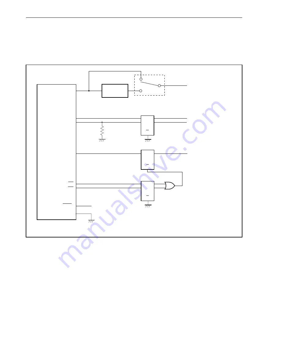
3.2.3 Interface Circuit and Cautions for ROM Probe
The interface circuit of the ROM probe is shown in Figure 3-6.
When using the ROM probe, note the cautions on designing the target system.
Figure 3-6. Interface Circuit Outline of ROM Probe
V
CC
A0 to A17
00-015
GND
(WORD/BYTE)
CE
OE
EP-16000C/EP-16384C
ROM socket (42-pin DIP)
DC-DC
Converter
Jumper switch
+3.3 V (to LVT244)
A18, A19
50 k
Ω
A
Y
G
LVT244
To IE-70000-MC-NW-A
To IE-70000-MC-NW-A
A
Y
G
LVT244
From IE-70000-MC-NW-A
A
Y
G
LVT244
OR gate
NC
Cautions 1. The bus load of the target system when the ROM probe is connected may be higher than
that when an actual ROM is connected. Caution must be paid when designing the bus of
the target system. It is recommended to mount a bus buffer in the ROM of the target
system.
2. A18 and A19 are pulled down (50 k
Ω
Ω
Ω
Ω
) inside the ROM probe, so they must be NC (no
connection) on the target system when they are not used on the target system.
3. When using the ROM emulation function, set the size of the ROM area set by the mapping
command of the debugger to the same size as the size of the ROM on the target system.
If these settings are different, the ROM emulation memory cannot be read with a correct
address from the target device.
4. Data cannot be written to the ROM emulation memory form the target device.
5. The access time of the ROM emulation memory is 60 ns. Set the wait count of the target
device to an appropriate value when using the ROM emulation memory.


