CHAPTER 4 CAUTIONS
28
4.2
NMI Signal
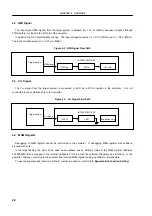
The input signal (NMI signal) from the target system is delayed (t
pD
= 10 ns (MAX.)) because it passes through
FPGA before it is input to the I/O chip of the emulator.
In addition, the DC characteristics change. The input voltage becomes V
IH
= 2.0 V (MIN.) and V
IL
= 0.8 V (MAX.).
The input current becomes I
IN
=
±
1.0
µ
A (MAX.).
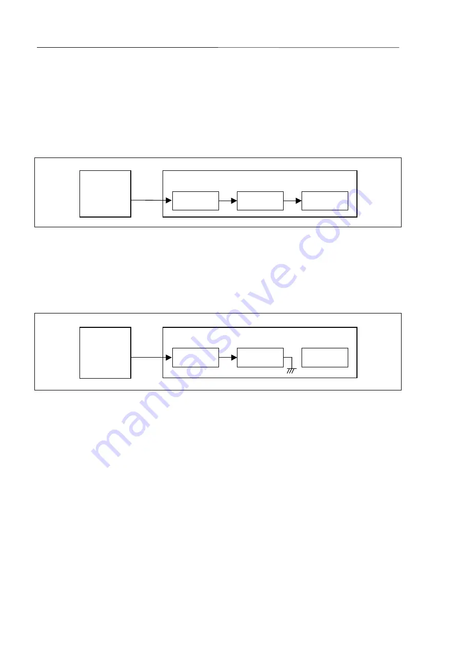
Figure 4-2. NMI Signal Flow Path
I/O chip
IE-703017-MC-EM1
NMI signal
Target system
NMI pin
FPGA
4.3
V
PP
Signal
The V
PP
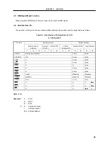
signal from the target system is connected to LED via a 330-
Ω
resistor in the emulator. It is not
connected to the evaluation chip in the emulator.
Figure 4-3. V
PP
Signal Flow Path
Evaluation chip
IE-703017-MC-EM1
V
PP
signal
Target system
330
Ω
LED
4.4
MAM Register
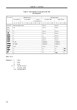
Debugging of MAM register cannot be performed in the emulator. If debugging MAM register with software,
proceed with care.
In the target device, the port can be used as an address bus by setting a value to the MAM register (address:
FFFFF068H) that is mapped in the internal peripheral I/O area with the software (Separate bus function). In the
emulator, however, switching to the separate bus through MAM register setting by software is impossible.
To use the separate bus function, set the J1 jumper in advance. (refer to 2.5 Separate Bus Function Setting)


