background image

User’s Manual  U16622EJ1V0UM

5

INTRODUCTION

Target Readers

This manual is intended for users who design and develop application systems

using the V850ES/SA2 and V850ES/SA3 microcontrollers.

Purpose

The purpose of this manual is to describe the basic specifications of the IE-

703204-G1-EM1 and its proper operation.

Organization

This manual is broadly divided into the following parts.

• Outline

•  Cautions

• Part names and functions

•  Restrictions

•  Setup procedure

How to Read This Manual

It is assumed that the reader of this manual has general knowledge in the fields of

electrical engineering, logic circuits, and microcontrollers.  Use the IE-703204-G1-EM1

connected to the in-circuit emulator (IE-V850ES-G1).  This manual describes the basic

setup procedures and switch settings of the IE-703204-G1-EM1 and IE-V850ES-G1.

For the part names, functions, and configuration parts of the IE-V850ES-G1, refer to the

IE-V850ES-G1 User’s Manual (U16313E)

 provided separately.

To learn about the basic specifications and operation

Read this manual in the order listed in 

CONTENTS

.

To learn software settings such as the operation methods, command functions, etc., of

the IE-V850ES-G1 or IE-703204-G1-EM1

Read the user’s manual of the debugger (sold separately) that is used.

Conventions

Note

:

Footnote for item marked with 

Note

 in the text

Caution

:

Information requiring particular attention

Remark

:

Supplementary information

Numeral representation:

Binary … 

××××

 or 

××××

B

Decimal ... 

××××

Hexadecimal ... 

××××

H

Prefix representing a power of 2 (address space, memory capacity):

K (kilo):

2

10

 = 1024

M (mega): 2

20

 = 1024

2

Terminology

The meanings of terms used in this manual are listed below.

Target device

This is the device to be emulated.

Target system

The system (user-built system) to be debugged.  This includes the target program and hardware

configured by the user.

Emulation CPU

The CPU that executes the program created by the user in the emulator.

Summary of Contents for IE-703204-G1-EM1

Page 1: ...User s Manual Target Devices V850ES SA2 V850ES SA3 IE 703204 G1 EM1 Emulation Board Document No U16622EJ1V0UM00 1st edition Date Published September 2003 N CP K Printed in Japan 2003 ...

Page 2: ...User s Manual U16622EJ1V0UM 2 MEMO ...

Page 3: ... of NEC Electronics products customers agree and acknowledge that the possibility of defects thereof cannot be eliminated entirely To minimize risks of damage to property or injury including death to persons arising from defects in NEC Electronics products customers must incorporate sufficient safety measures in their design such as redundancy fire containment and anti failure features NEC Electro...

Page 4: ...nch Seoul Korea Tel 02 558 3737 NEC Electronics Shanghai Ltd Shanghai P R China Tel 021 6841 1138 NEC Electronics Taiwan Ltd Taipei Taiwan Tel 02 2719 2377 NEC Electronics Singapore Pte Ltd Novena Square Singapore Tel 6253 8311 J03 4 NEC Electronics Europe GmbH Duesseldorf Germany Tel 0211 65 03 01 Sucursal en España Madrid Spain Tel 091 504 27 87 Vélizy Villacoublay France Tel 01 30 67 58 00 Succ...

Page 5: ... and configuration parts of the IE V850ES G1 refer to the IE V850ES G1 User s Manual U16313E provided separately To learn about the basic specifications and operation Read this manual in the order listed in CONTENTS To learn software settings such as the operation methods command functions etc of the IE V850ES G1 or IE 703204 G1 EM1 Read the user s manual of the debugger sold separately that is us...

Page 6: ... B 4 5 6 4 3 5 0 6 5 4 6 4 C 0 D 0 0 0 1 3 D 1 1 C B B D 9 1 2E D 52 6 2E 1 52 6 2 3 2 1 3 C F 1 G 1 71 7 1 0 01 2 3 4 2 ...

Page 7: ... 17 2 1 Part Names and Functions of IE 703204 G1 EM1 17 2 2 LEDs Controlled by IE 703204 G1 EM1 19 CHAPTER 3 SETUP PROCEDURE 20 3 1 Connecting IE V850ES G1 and IE 703204 G1 EM1 with Probe 20 3 2 Replacing Resonator 23 CHAPTER 4 CAUTIONS 24 4 1 Connection with Target System 24 4 2 Characteristics of Target Interface 24 CHAPTER 5 RESTRICTIONS 34 5 1 Clock Generator 34 5 2 Timing of Setting Releasing...

Page 8: ...ontrolled by IE 703204 G1 EM1 19 4 1 Equivalent Circuit A 24 4 2 Equivalent Circuit B 24 4 3 Equivalent Circuit C 25 4 4 Equivalent Circuit D 25 4 5 Equivalent Circuit E 25 4 6 Equivalent Circuit F 25 4 7 Equivalent Circuit G 26 4 8 Equivalent Circuit H 26 4 9 Equivalent Circuit I 26 4 10 Equivalent Circuit J 26 4 11 Equivalent Circuit K 27 4 12 Equivalent Circuit L 27 ...

Page 9: ...User s Manual U16622EJ1V0UM 9 LIST OF TABLES Figure No Title Page 4 1 Pin Correspondence List V850ES SA2 Pin Names 28 4 2 Pin Correspondence List V850ES SA3 Pin Names 31 ...

Page 10: ...03204 G1 EM1 can be used for efficient hardware and software debugging during system development using the V850ES SA2 and V850ES SA3 This manual describes the basic setup procedure and the switch settings of the IE V850ES G1 when connected to the IE 703204 G1 EM1 For the part names and functions of the IE V850ES G1 refer to the separate IE V850ES G1 User s Manual U16313E ...

Page 11: ... by installing the IE 703204 G1 EM1 board PC interface board IE 70000 PCI IF A IE 70000 CD IF A This is a board for connecting the IE V850ES G1 to a PC More than one such board can be installed using the PC s expansion slots IE 70000 PCI IF A For PCI bus IE 70000 CD IF A For PCMCIA socket SWEX 100SD 1 SWEX 120SE 1 General purpose probes made by TOKYO ELETECH CORPORATION Separately sold products So...

Page 12: ...n Connected to IE V850ES G1 Maximum operating frequency 20 MHz 2 2 V to 2 7 V The following pins can be masked NMI WAIT RESET HLDRQ The external dimensions of the IE 703204 G1 EM1 are listed below Item Value Height 35 mm Width 205 mm External dimensions Depth 140 mm ...

Page 13: ...External memory 1 MB Internal ROM 256 KB Branch destination entry count calculation coverage memory capacity External memory 1 MB Trace memory capacity 168 bits 32 K frames Time measurement function Internal timers 3 8 bit external trace possible External logic probe Trace break event setting possible Event break Step execution break Forced break Break function Fail safe break Illegal access to pe...

Page 14: ...ely device file obtained separately Note 1 3 PC interface board IE 70000 PCI IF A IE 70000 CD IF A Sold separately 4 PC interface cable supplied with IE V850ES G1 Sold separately 5 IE V850ES G1 sold separately 6 Emulation board this product 7 ProbeNote 2 SWEX 120SE 1 Sold separately 8 ProbeNote 2 SWEX 100SD 1 Sold separately 9 CSICE121A1312N03Note 2 sold separately 10 LSPACK121A1312N01Note 2 sold ...

Page 15: ...pply cable supplied with IE V850 G1 Sold separately Notes 1 The device file can be downloaded from the NEC Electronics website URL http www necel com micro 2 These are products of TOKYO ELETECH CORPORATION For further information contact Daimaru Kogyo Co Ltd Tokyo Electronics Department TEL 81 3 3820 7112 Osaka Electronics Department TEL 81 6 6244 6672 ...

Page 16: ...ics sales representative or distributor Figure 1 2 Contents in Carton 3 Guaranteed card 4 Packing list 1 IE 703204 G1 EM1 2 Accessory bag 1 IE 703204 G1 EM1 1 2 Accessory bag 1 3 Guarantee card 1 4 Packing list 1 Check whether the accessory bag contains the following items in addition to this manual and the packing list 1 a 7 pin header for resonator replacement 1 b NQPACK100SD for mounting board ...

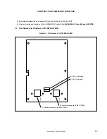
Page 17: ...he IE 703204 G1 EM1 For the part names and functions of the IE V850ES G1 refer to the IE V850ES G1 User s Manual U16313E 2 1 Part Names and Functions of IE 703204 G1 EM1 Figure 2 1 Part Names of IE 703204 G1 EM1 1 Socket for connecting SWEX 100SD 1 4 OSC2 subclock 3 OSC1 main clock 1 1 2 Socket for connecting SWEX 120SE 1 ...

Page 18: ...g the IE 703204 G1 EM1 as the emulator of the V850ES SA3 3 OSC1 main clock This is the socket in which the resonator that generates the main clock is mounted Use this socket when replacing the resonator for the main clock For details refer to 3 2 Resonator Replacement 4 OSC2 subclock This is the socket in which the resonator that generates the subclock is mounted The frequency of the subclock is f...

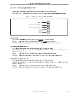
Page 19: ...al is inactive VDD level 2 Target VDD supply voltage 1 The status of the VDD signal connected to the target system is indicated as follows This LED indicates the status of pin 11 during V850ES SA2 emulation and the status of the F3 pin during V850ES SA3 emulation Lit ON The target system is connected and voltage is being applied to the VDD pin Unlit OFF Either the target system is not connected or...

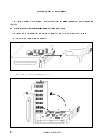
Page 20: ...G1 EM1 to related products and how to replace the resonator 3 1 Connecting IE V850ES G1 and IE 703204 G1 EM1 with Probe The following shows the procedure to connect the IE V850ES G1 and IE 703204 G1 EM1 with the probe 1 Pull off the front cover of the IE V850ES G1 2 Raise the frame of the IE V850ES G1 as shown ...

Page 21: ...rs on each side At this time align the board so that the socket YQSOCKET to connect the prove faces towards the probe exit side Insert the probe SWEX 100SD 1 or SWEX 120SE 1 in the socket corresponding to the target device refer to the following figure Socket to connect SWEX 120SE 1 for V850ES SA3 Socket to connect SWEX 100SD 1 for V850ES SA2 ...

Page 22: ...CHAPTER 3 SETUP PROCEDURE User s Manual U16622EJ1V0UM 22 4 Slowly lower the frame of the IE V850ES G1 5 Replace the front cover of the IE V850ES G1 ...

Page 23: ... OSC2 subclock 32 768 kHz oscillator To change the main clock frequency mount the resonator and capacitor on the included 7 pin header as shown and substitute it for the 7 pin header already mounted on OSC1 main clock 1 2 3 4 5 6 7 7 pin header Open 1 2 3 4 5 6 7 7 pin socket Open µPD70F3204Y Emulation CPU X1 X2 OSC1 main clock The frequency of the subclock is fixed to 32 768 kHz so the resonator ...

Page 24: ...unctionally operates as if an actual device is connected however the characteristics may be different than those of the actual device The target interface of the IE 703204 G1 EM1 is one of those shown in Figures 4 1 to 4 12 The target interface processing of each target device is shown in Tables 4 1 and 4 2 Figure 4 1 Equivalent Circuit A PD70F3204Y Emulation CPU Port pin Target system side IE sys...

Page 25: ...ser reset pin Target system side IE system side P174AVC16245 Voltage level shifter A B 3 6 V Same potential as VDD Same potential as VDD VCCB VCCA µ Figure 4 5 Equivalent Circuit E PD70F3204Y Emulation CPU AVREF0 AVREF1 G6H 2F Relay Note Target system side IE system side P174AVC16245 Voltage level shifter A B 3 6 V Same potential as VDD VCCB VCCA µ Note Conducts only when the target system is conn...

Page 26: ... when the target system is connected Figure 4 8 Equivalent Circuit H EP1K100FC484 FPGA 1 MΩ II Target system side IE system side P174AVC16245 Voltage level shifter A B 3 6 V Same potential as VDD VCCB VCCA Figure 4 9 Equivalent Circuit I Target system side AVDD IE system side PD70F3204Y Emulation CPU AVDD EVDD EVDD Open Open N C Same potential as VDD Open µ Figure 4 10 Equivalent Circuit J IE syst...

Page 27: ...Circuit K Target system side AVSS IE system side PD70F3204Y Emulation CPU AVSS VSS EVSS VSS EVSS µ Figure 4 12 Equivalent Circuit L IE system side Target system side X2 X1 Open Open XT2 XT1 Open Open PD70F3204 Emulation CPU XT1 XT2 1 27 pF 7 1 7 27 pF 32 768 kHz X1 X2 1 MΩ µ ...

Page 28: ...ation circuit D 16 XT1 Emulation circuit L 17 XT2 Emulation circuit L 18 VDD Emulation circuit G 19 VSS Emulation circuit K 20 P90 A0 Emulation circuit C 21 P91 A1 Emulation circuit C 22 P92 A2 INTP5 Emulation circuit C 23 P93 A3 INTP6 Emulation circuit C 24 P94 A4 TO2 Emulation circuit C 25 P95 A5 TO3 Emulation circuit C 26 P96 A6 TO4 Emulation circuit C 27 P97 A7 TO5 Emulation circuit C 28 P98 A...

Page 29: ...PDL3 AD3 Emulation circuit B 56 PDL4 AD4 Emulation circuit B 57 PDL5 AD5 FLMD1 Emulation circuit B 58 PDL6 AD6 Emulation circuit B 59 PDL7 AD7 Emulation circuit B 60 PDL8 AD8 Emulation circuit B 61 PDL9 AD9 Emulation circuit B 62 IC FLMD0 Emulation circuit B 63 EVSS Emulation circuit K 64 EVDD Emulation circuit I 65 PDL10 AD10 Emulation circuit B 66 PDL11 AD11 Emulation circuit B 67 PDL12 AD12 Emu...

Page 30: ...tion circuit A 85 P02 INTP1 TI3 Emulation circuit A 86 P03 INTP2 TI4 Emulation circuit A 87 P04 INTP3 TI5 Emulation circuit A 88 P05 INTP4 Emulation circuit A 89 P711 ANI11 Emulation circuit A 90 P710 ANI10 Emulation circuit A 91 P79 ANI9 Emulation circuit A 92 P78 ANI8 Emulation circuit A 93 P77 ANI7 Emulation circuit A 94 P76 ANI6 Emulation circuit A 95 P75 ANI5 Emulation circuit A 96 P74 ANI4 E...

Page 31: ...F0 Emulation circuit E B3 P72 ANI2 Emulation circuit A B4 P712 ANI12 Emulation circuit A B5 P75 ANI5 Emulation circuit A B6 P77 ANI7 Emulation circuit A B7 P710 ANI10 Emulation circuit A B8 PCD3 Emulation circuit B B9 P02 INTP1 TI3 Emulation circuit A B10 P46 INTP11 TO1 Emulation circuit A B11 P42 SCK0 SCL Emulation circuit A B12 P40 SI0 Emulation circuit A B13 PDH4 A20 Emulation circuit B C1 P80 ...

Page 32: ...n circuit F F11 PDL11 AD11 Emulation circuit B F12 PDL13 AD13 Emulation circuit B F13 PDL12 AD12 Emulation circuit B G1 RESET Emulation circuit D G2 XT1 Emulation circuit L G3 X2 Emulation circuit L G11 EVSS Emulation circuit K G12 PDL10 AD10 Emulation circuit B G13 EVDD Emulation circuit I H1 VSS Emulation circuit K H2 VDD Emulation circuit G H3 XT2 Emulation circuit L H11 PDL8 AD8 Emulation circ...

Page 33: ...ation circuit B M1 P95 A5 TO3 Emulation circuit C M2 P97 A7 TO5 Emulation circuit C M3 P99 A9 TXD1 Emulation circuit C M4 P913 A13 SI3 Emulation circuit C M5 EVSS Emulation circuit K M6 PCS5 Emulation circuit H M7 PCS4 Emulation circuit H M8 PCM0 WAIT Emulation circuit B M9 PCM2 HLDAK Emulation circuit B M10 PCT3 Emulation circuit H M11 PCT4 RD Emulation circuit B M12 PCT7 Emulation circuit B M13 ...

Page 34: ...however there may be a period in which the clock is not initialized to fXX 8 with the in circuit emulator depending on the timing of reset release 5 2 Timing of Setting Releasing Standby Mode The timing of setting releasing the standby mode is different between the target device and the in circuit emulator The difference is within 1 clock when standby mode is set and 2 or 3 clocks when it is relea...

Page 35: ...0 14 0 2 5 2 5 0 5 X 24 12 0 5 8 0 3 Slit width 3 R 2 2 0 5 0 1 0 16 6 13 0 20 2 5 8 3 1 0 φ SIDE VIEW 0 18 15 0 0 5 0 5 0 2 1 85 5 1 5 5 1 2 3 7 9 45 3 9 1 85 BOTTOM VIEW 17 0 9 0 0 2 Slit width 15 0 16 0 14 0 4 2 0 Projection height 1 8 φ Remark NQPACK100SD is a product of TOKYO ELETECH CORPORATION ...

Page 36: ... VIEW 3 1 0 4 R 3 2 φ 4 2 2 φ 4 R 2 2 13 4 21 0 23 0 16 6 10 9 13 3 15 7 18 1 0 5 X 24 12 0 5 8 0 5 5 8 SIDE VIEW 0 25 0 4 7 4 3 1 2 3 1 2 3 9 3 1 2 2 3 7 9 0 2 5 0 25 X 0 3 0 3 BOTTOM VIEW 13 4 15 3 16 1 14 1 0 2 17 3 C 1 5 Remark YQPACK100SD is a product of TOKYO ELETECH CORPORATION ...

Page 37: ... HQPACK100SD unit mm TOP VIEW 3 1 0 R 3 2 φ 4 2 2 φ R 2 2 13 4 21 0 23 0 16 6 0 5 X 24 12 0 5 8 0 5 5 8 SIDE VIEW 0 23 0 58 7 4 3 1 2 3 1 2 3 9 1 6 2 15 BOTTOM VIEW 13 4 15 12 17 1 14 1 0 2 17 3 C 1 5 Remark HQPACK100SD is a product of TOKYO ELETECH CORPORATION ...

Page 38: ...29 11 6 12 1 14 7 17 3 19 9 Pin 1 side 4 2 2 φ 3 3 φ Part hole C2 SIDE VIEW 4 1 03 2 4 3 9 0 8 8 1 0 32 φ φ BOTTOM VIEW A N 1 13 MADE IN JAPAN TET CSICE121A1312N03 CSI PWB 121A1312N01 Resist diameter 0 5 φ 121 land diameter 0 5 φ 0 8 0 8X12 9 6 0 8 0 8X12 9 6 4 3 Remark CSICE121A1312N03 is a product of TOKYO ELETECH CORPORATION ...

Page 39: ...r s Manual U16622EJ1V0UM 39 5 LSPACK121A1312N01 unit mm TOP VIEW 29 22 65 0 8 0 8X12 9 6 0 8 0 8X12 9 6 TET MADE IN JAPAN LSPACK121A SIDE VIEW 1 65 6 7 1 BOTTOM VIEW Remark LSPACK121A1312N01 is a product of TOKYO ELETECH CORPORATION ...

Page 40: ... Manual U16622EJ1V0UM 40 6 CSSOCKET121A1312N01 unit mm TOP VIEW 0 8 4 0 8X12 9 6 C1 Pin 1 side 0 8 9 6 0 8X12 9 6 4 12 SIDE VIEW 3 4 2 2 5 8 1 1 2 0 65 0 25 0 7 φ φ φ Remark CSSOCKET121A1312N01 is a product of TOKYO ELETECH CORPORATION ...

Page 41: ...User s Manual U16622EJ1V0UM 41 7 CSSOCKET121A1312N01N unit mm TOP VIEW 0 8 4 0 8X12 9 6 C1 Pin 1 side 0 8 9 6 0 8X12 9 6 4 12 SIDE VIEW 3 4 2 1 2 0 65 0 25 φ φ Remark CSSOCKET121A1312N01N is a product of TOKYO ELETECH CORPORATION ...

Page 42: ...ser s Manual U16622EJ1V0UM 42 8 CSSOCKET121A1312N01S1 unit mm TOP VIEW 0 8 4 0 8X12 9 6 C1 Pin 1 side 0 8 9 6 0 8X12 9 6 4 12 SIDE VIEW 3 4 2 1 2 0 65 0 25 φ φ Remark CSSOCKET121A1312N01S1 is a product of TOKYO ELETECH CORPORATION ...

Page 43: ... 0 8X12 9 6 External dimensions of CSSOCKET 12 23 0 8X12 9 6 Remarks 1 After CSSOCKET has been fixed on the board by soldering it is recommended to solder the guide pin of the connector from the lower side of the board or to fix the portion around the connector with resin for reinforcement 2 The soldering reflow conditions are the same as for the CSPACK Remark CSSOCKET121A1312N01 is a product of T...

Page 44: ... TOP VIEW TET JAPAN 295 8 48 48 38 5 38 5 6 13 1 19 5 6 4 20 13 1 19 5 20 Ground Wire TET CN2 CN4 FG SG FG SG FG SG FG SG 1 25 50 51 75 76 5 45 Black Red 26 CN1 CN3 Target 100 IC1 f SWEX 100SD1 MADE IN JAPAN SWEX 100SD E2 Remark SWEX 100SD 1 is a product of TOKYO ELETECH CORPORATION ...

Page 45: ...P VIEW TET JAPAN 55 5 47 5 TET MADE IN JAPAN 55 5 47 5 CN4 1 36 37 72 73 108 109 144 FG FG SG FG SG FG 19 5 24 295 8 7 6 4 12 5 19 5 24 12 5 5 45 Black Red Ground Wire f SWEX 144SD 1 Target CN2 CN3 CN1 SWEX 144SD E2 Remark SWEX 120SE 1 is a product of TOKYO ELETECH CORPORATION SIDE VIEW ...

Reviews: