125
CHAPTER 5 PORT FUNCTIONS
User’s Manual U12697EJ3V0UM
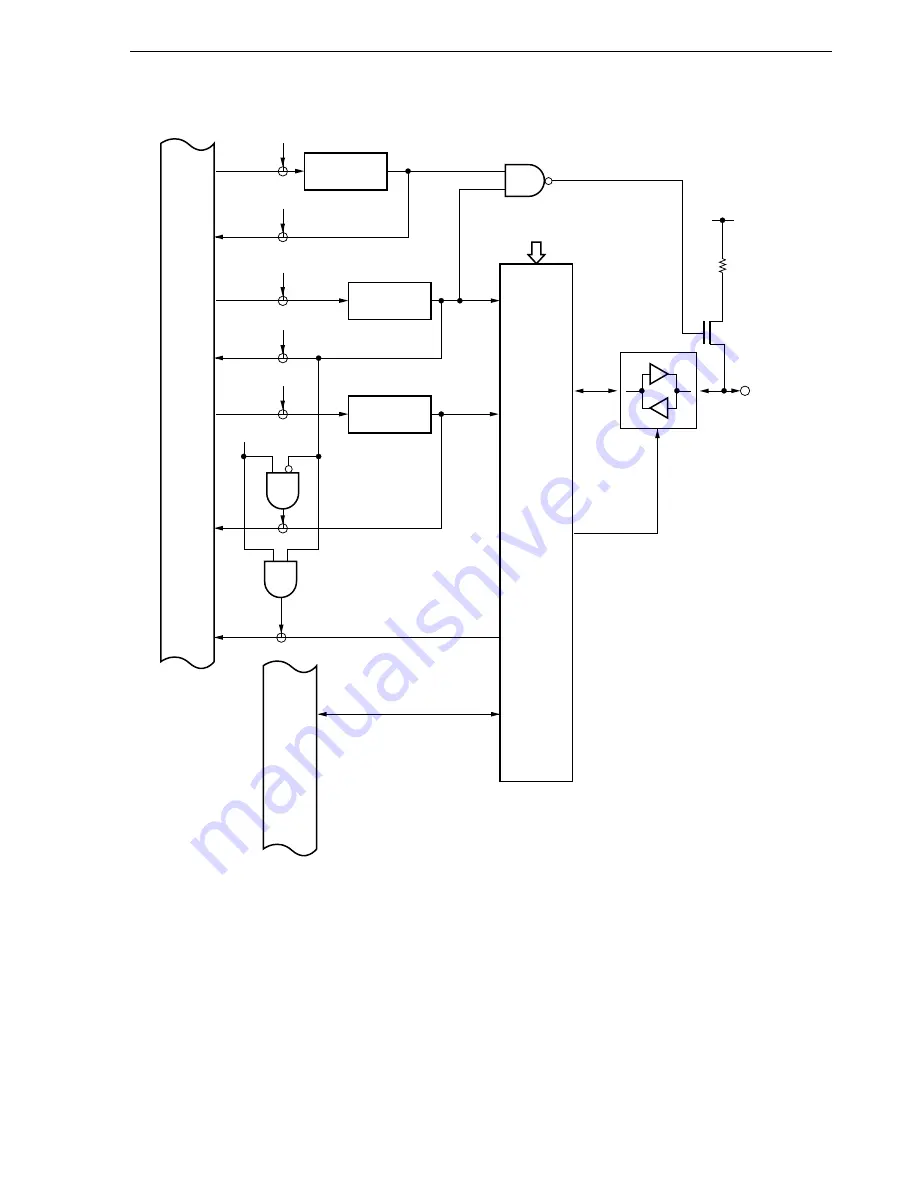
Figure 5-12. Block Diagram of P60 to P63
PUO: Pull-up resistor option register
PM:
Port mode register
RD:
Port 6 read signal
WR:
Port 6 write signal
MM0 to MM3: Bits 0 to 3 of the memory expansion mode register (MM)
WR
PU0
PUO6
WR
PM6
PM60 to PM63
RD
PU0
WR
P6
RD
P6
Output latch
(P60 to P63)
RD
PM6
V
DD
P60/A16 to
P63/A19
Internal address bus
Internal data bus
I/O controller
MM0 to MM3


