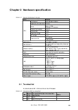
Table 3-6 On-chip debug mode settings for the TK-850/SG2+UZ
SW1
Bit 1
ON
Bit 2
ON
Bit 3
ON
Bit 4
OFF
JP1
USB side (1-2-pin short)
3.2.1.3
N-Wire Connecting Mode
Change to the following settings when you connect to N-Wire emulator to the
TK-850/SG2+UZ board.
Table 3-7 N-wire connecting mode settings for the TK-850/SG2-UZ
SW1
Bit 1
ON or OFF
Note
Bit 2
OFF
Bit 3
OFF
Bit 4
OFF
JP1
USB side (1-2-pin short)
Note: Please set ON, if you make COM communication to host machine using the
P30/TXDA0,P31/RXDA0 pin.
3.2.1.4
Normal Operation Mode
Change to the following settings when you execute the program normally. Select
the power source chosen with the JP1.
Table 3-8 Normal operation mode settings for the TK-850/SG2+UZ
SW1
Bit 1
OFF
Bit 2
OFF
Bit 3
OFF
Bit 4
OFF
JP1
USB powered (1-2-pin short)
Battery powered with CN2 (2-3-pin short)
3.2.1.5
General purpose setting port
Bit 5, 6, 7 and 8 of SW1 are general purpose setting ports.
The port state is “Low” because it is connected to GND when the switch is ON.
The port state is “High” because it is connected to a 10kΩ pull-up resistor, when
the switch is OFF.
Table 3-9 Switch SW1 terminal list
SW1
Signal name
Terminal CPU name at connection destination
Bit 5
P74
P74/ANI4
Bit 6
P75
P75/ANI5
Bit 7
P76
P76/ANI6
Bit 8
P77
P77/ANI7
Hardware specification
Chapter 3
User's Manual U19026EE3V0UM00
23


