1047
User’s Manual U16580EE3V1UD00
Appendix B
Revision History
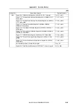
The following shows the revision history up to present. Application portions signifies the chapter of each
edition.
(1/5)
Edition No.
Major items revised
Revised Sections
EE2
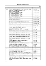
Due to the new guideline of wording and terminology,
the nickname “PHOENIX-F” removed throughout the UM
whole User’s Manual
“Burst flash memory” removed throughout the UM
whole User’s Manual
BCLK (Burst clock output), STST and STNXT ((Burst control output)
removed
whole User’s Manual
1.4 “Ordering Information”, Note deleted
1.4, p.35
Figure 1-1 “Pin Configuration 208-pin Plastic LQFP” changed
1.5, p. 36
Table 1-1 “256-pin Plastic BGA” changed
1.5, p.38
Section “Pin identification” changed
1.5, p.40
Figure 1-3 “Internal Block Diagram” changed
1.6.1, p.41
Table 2-1 “Port Pins” changed
2.1, p.48
Table 2-2 “Non-Port Pins” changed
2.1, p.50, p.52
Table 3-5 “Peripheral I/O Registers” changed
3.4.6, p.101, 104, 107
Figure 3-20 “Programmable Peripheral Area Control Register BPC” bits 13
and 12 changed
3.4.7 (1), p.112
3.4.8 (1), Setting data to specific registers changed, Caution 2 added
3.4.8 (1), p.127
3.4.10, DMA wait control register 0 (DMAWC0) set value changed
3.4.10, p.130
Figure 4-11 “Bus Clock Dividing Control Register (DVC)” address value
changed
4.7 (2), p.166
Table 3-5 “Peripheral I/O Registers” changed
3.4.6, p.101, 104, 107
Chapter 5.2 “Burst Mode Flash” removed
5.2, p.180
6.1 “Features of the DMA” added
6.1, p.181
Figure 6-1 “DMA Transfer Memory Start Address Registers 0 to 7 (MAR0 to
MAR7)”, Caution 2 added
6.2 (1), p.182
Figure 6-2 “DMA Transfer SFR Start Address Registers 2, 3 (SAR2,
SAR3)”, Caution added
6.2 (2), p.183
Figure 6-3 “DMA Transfer Count Registers 0 to 7 (DTCR0 to DTCR7)”,
Caution 3 deleted
6.2 (3), p.184
Figure 6-8 “Initialization of DMA Transfer for A/D Conversion Result”
changed
6.4.1, p.189
Figure 6-9 “Operation of DMA Channel 0/1” added
6.4.1, p.190
Figure 6-10 “DMA Channel 0 and 1 Trigger Signal Timing”, added
6.4.1, p.191
6.4.2 “DMA transfer of PWM timer reload (TMR0, TMR1)”,
DMA trigger count changed
6.4.2, p.192
Figure 6-11 “Initialization of DMA Transfer for TMRn Compare Registers”,
changed
6.4.2, p.193
Figure 6-12 “Operation of DMA Channel 2/3”, added
6.4.2, p.194
Figure 6-13 “DMA Channel 2 and 3 Trigger Signal Timing”, added
6.4.2, p.195
Table 6-2 “DMA Configuration of Serial Data Reception”,
DMA trigger factor changed
6.4.3 (1), p.196
Summary of Contents for V850E/PH2
Page 6: ...6 Preface User s Manual U16580EE3V1UD00...
Page 16: ...16 User s Manual U16580EE3V1UD00...
Page 28: ...28 User s Manual U16580EE3V1UD00...
Page 32: ...32 User s Manual U16580EE3V1UD00...
Page 84: ...84 Chapter 2 Pin Functions User s Manual U16580EE3V1UD00 MEMO...
Page 144: ...144 Chapter 3 CPU Functions User s Manual U16580EE3V1UD00 MEMO...
Page 192: ...192 Chapter 5 Memory Access Control Function PD70F3187 only User s Manual U16580EE3V1UD00 MEMO...
Page 312: ...312 Chapter 9 16 Bit Timer Event Counter P User s Manual U16580EE3V1UD00 MEMO...
Page 534: ...534 Chapter 11 16 bit Timer Event Counter T User s Manual U16580EE3V1UD00...
Page 969: ...969 Chapter 20 Port Functions User s Manual U16580EE3V1UD00 MEMO...
Page 970: ...970 Chapter 20 Port Functions User s Manual U16580EE3V1UD00...
Page 976: ...976 Chapter 22 Internal RAM Parity Check Function User s Manual U16580EE3V1UD00 MEMO...
Page 984: ...984 Chapter 23 On Chip Debug Function OCD User s Manual U16580EE3V1UD00 MEMO...
Page 1006: ...1006 Chapter 24 Flash Memory User s Manual U16580EE3V1UD00 MEMO...
Page 1036: ...1036 Chapter 27 Recommended Soldering Conditions User s Manual U16580EE3V1UD00 MEMO...
Page 1046: ...1046 Appendix A Index User s Manual U16580EE3V1UD00 MEMO...
Page 1052: ...1052 User s Manual U16580EE3V1UD00...
Page 1053: ......


