635
Chapter 15
Asynchronous Serial Interface C (UARTC)
User’s Manual U16580EE3V1UD00
15.5.7 UART
receive
operation
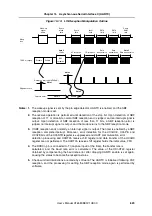
The reception wait status is set by setting the UCnPWR bit of the UCnCTL0 register to 1 and then
setting the UCnRX bit of the UCnCTL0 register to 1. In the reception wait status, the RXDCn pin is
monitored and start bit detection is performed.
Start bit detection is performed using a two-step detection routine.
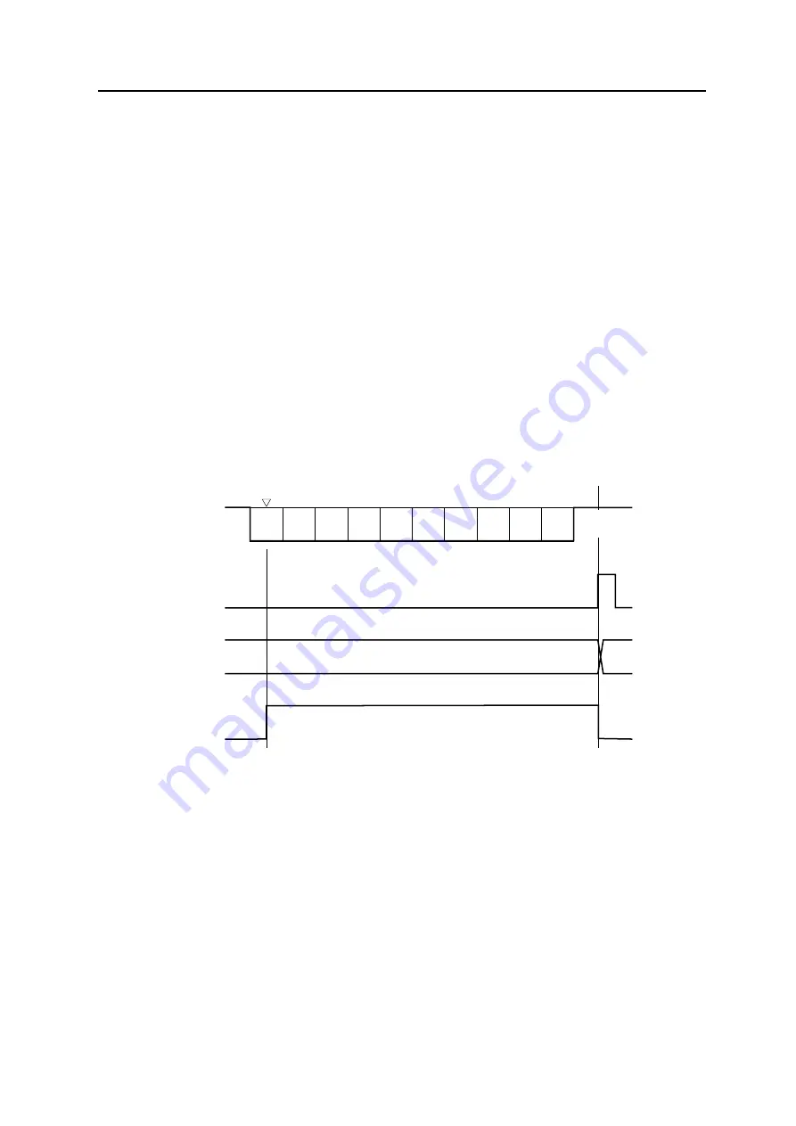
First, an 8-bit counter starts upon detection of the falling edge of the RXDCn pin. When the 8-bit
counter has counted the UCnCTL2 register setting value, the level of the RXDCn pin is monitored again
(corresponds to the
∇
mark in Figure 15-19). If the RXDCn pin is low level at this time too, a start bit is
recognized. After a start bit has been recognized, the receive operation starts, and serial data is saved
to the UARTCn receive shift register according to the set baud rate. Additionally the UCnRSF flag of
UCnSTR1 register is set (1) to indicate the receive operation status.
When the reception complete interrupt (INTUCnR) is output upon reception of the stop bit, the data of
the UARTCn receive shift register is written to the UCnRX register, and the UCnRSF flag is cleared (0)
simultaneously. However, if an overrun error occurs (UCnOVE bit = 1), the receive data at this time is
not written to the UCnRX register, and a reception error interrupt (INTUCnRE) is output.
Even if a parity error (UCnPE bit = 1) or a framing error (UCnFE bit = 1) occurs during reception,
reception continues until the stop bit reception position, but a reception error interrupt (INTUCnRE) is
output following reception completion.
Figure 15-19:
UART Reception Timing
Cautions: 1. Be sure to read the UCnRX register even when a reception error occurs. If the
UCnRX register is not read, an overrun error occurs during reception of the next
data, and reception errors continue occurring indefinitely.
2. The operation during reception is performed assuming that there is only one stop
bit. A second stop bit is ignored.
Start
bit
D0
D1
D2
D3
D4
D5
D6
D7
Parity
bit
Stop
bit
INTUCnR
UCnRX
UCnRSF
Summary of Contents for V850E/PH2
Page 6: ...6 Preface User s Manual U16580EE3V1UD00...
Page 16: ...16 User s Manual U16580EE3V1UD00...
Page 28: ...28 User s Manual U16580EE3V1UD00...
Page 32: ...32 User s Manual U16580EE3V1UD00...
Page 84: ...84 Chapter 2 Pin Functions User s Manual U16580EE3V1UD00 MEMO...
Page 144: ...144 Chapter 3 CPU Functions User s Manual U16580EE3V1UD00 MEMO...
Page 192: ...192 Chapter 5 Memory Access Control Function PD70F3187 only User s Manual U16580EE3V1UD00 MEMO...
Page 312: ...312 Chapter 9 16 Bit Timer Event Counter P User s Manual U16580EE3V1UD00 MEMO...
Page 534: ...534 Chapter 11 16 bit Timer Event Counter T User s Manual U16580EE3V1UD00...
Page 969: ...969 Chapter 20 Port Functions User s Manual U16580EE3V1UD00 MEMO...
Page 970: ...970 Chapter 20 Port Functions User s Manual U16580EE3V1UD00...
Page 976: ...976 Chapter 22 Internal RAM Parity Check Function User s Manual U16580EE3V1UD00 MEMO...
Page 984: ...984 Chapter 23 On Chip Debug Function OCD User s Manual U16580EE3V1UD00 MEMO...
Page 1006: ...1006 Chapter 24 Flash Memory User s Manual U16580EE3V1UD00 MEMO...
Page 1036: ...1036 Chapter 27 Recommended Soldering Conditions User s Manual U16580EE3V1UD00 MEMO...
Page 1046: ...1046 Appendix A Index User s Manual U16580EE3V1UD00 MEMO...
Page 1052: ...1052 User s Manual U16580EE3V1UD00...
Page 1053: ......

