651
Chapter 16
Clocked Serial Interface B (CSIB)
User’s Manual U16580EE3V1UD00
(2)
CSIBn control register 1 (CBnCTL1)
The CBnCTL1 register is an 8-bit register that controls the CSIB serial transfer operation.
This register can be read or written in 8-bit or 1-bit units.
Reset input clears this register to 00H.
Caution:
The CBnCTL1 register can be rewritten when the CBnPWR bit of the CBnCTL0
register is 0 or when both the CBnTXE and CBnRXE bits are 0.
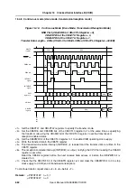
Figure 16-5:
CSIBn Control Register 1 (CBnCTL1)
Notes: 1.
For details on the baud rate generator refer to
16.7 ”Baud Rate Generator” on page 673
2.
Not available on
μ
PD70F3447
Remark:
μ
PD70F3187:
n = 0, 1
μ
PD70F3447:
n = 0
After reset:
00H
R/W
Address:
CB0CTL1 FFFFFD01H,
CB1CTL1 FFFFFD21H
Note 2
7
6
5
4
3
2
1
0
CBnCTL1
0
0
0
CBnCKP
CBnDAP CBnCKS2 CBnCKS1 CBnCKS0
CBnCKP
CBnDAP
Specification of Data Transmission/Reception Timing in Relation to
Clock Phase
0
0
0
1
1
0
1
1
CBnCKS2 CBnCKS1 CBnCKS0
Base Clock (f
XCCLK
)
Mode
0
0
0
f
BRG0
Note 1
Master mode
0
0
1
f
BRG1
Note 1
Master mode
0
1
0
f
XX
/8
Master mode
0
1
1
f
XX
/16
Master mode
1
0
0
f
XX
/32
Master mode
1
0
1
f
XX
/64
Master mode
1
1
0
f
XX
/128
Master mode
1
1
1
External clock (SCKBn)
Slave mode
D7
D6
D5
D4
D3
D2
D1
D0
SCKBn (I/O)
SIBn capture
SOBn (output)
D7
D6
D5
D4
D3
D2
D1
D0
SCKBn (I/O)
SIBn capture
SOBn (output)
D7
D6
D5
D4
D3
D2
D1
D0
SCKBn (I/O)
SIBn capture
(output)
D7
D6
D5
D4
D3
D2
D1
D0
SCKBn (I/O)
SIBn capture
(output)
Summary of Contents for V850E/PH2
Page 6: ...6 Preface User s Manual U16580EE3V1UD00...
Page 16: ...16 User s Manual U16580EE3V1UD00...
Page 28: ...28 User s Manual U16580EE3V1UD00...
Page 32: ...32 User s Manual U16580EE3V1UD00...
Page 84: ...84 Chapter 2 Pin Functions User s Manual U16580EE3V1UD00 MEMO...
Page 144: ...144 Chapter 3 CPU Functions User s Manual U16580EE3V1UD00 MEMO...
Page 192: ...192 Chapter 5 Memory Access Control Function PD70F3187 only User s Manual U16580EE3V1UD00 MEMO...
Page 312: ...312 Chapter 9 16 Bit Timer Event Counter P User s Manual U16580EE3V1UD00 MEMO...
Page 534: ...534 Chapter 11 16 bit Timer Event Counter T User s Manual U16580EE3V1UD00...
Page 969: ...969 Chapter 20 Port Functions User s Manual U16580EE3V1UD00 MEMO...
Page 970: ...970 Chapter 20 Port Functions User s Manual U16580EE3V1UD00...
Page 976: ...976 Chapter 22 Internal RAM Parity Check Function User s Manual U16580EE3V1UD00 MEMO...
Page 984: ...984 Chapter 23 On Chip Debug Function OCD User s Manual U16580EE3V1UD00 MEMO...
Page 1006: ...1006 Chapter 24 Flash Memory User s Manual U16580EE3V1UD00 MEMO...
Page 1036: ...1036 Chapter 27 Recommended Soldering Conditions User s Manual U16580EE3V1UD00 MEMO...
Page 1046: ...1046 Appendix A Index User s Manual U16580EE3V1UD00 MEMO...
Page 1052: ...1052 User s Manual U16580EE3V1UD00...
Page 1053: ......


