683
Chapter 17
Clocked Serial Interface 3 (CSI3)
User’s Manual U16580EE3V1UD00
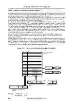
Figure 17-3:
Clocked Serial Interface Clock Select Register 3n (CSIC3n) (2/3)
Note:
If the CKPn bit is set to 1 in the master mode (CKS3n2 to CKS3n0 bits are other than 111B), the
SCK3n pin outputs a low level when it is inactive. If the CTXEn bit of the CSIM3n register is
cleared to 0 (disabling transmission) and CRXEn bit is cleared to 0 (disabling reception), the
SCK3n pin outputs a high level.
Therefore, take the following measures to fix the SCK3n pin to low level when CSI3n is not
used.
[SCK3n pin]
<1> Clear the corresponding port bit (P82 of the P8 register for CSI30, or P92 of the P9 register
for CSI31) to 0:
The port output level is set to low.
<2> Clear the corresponding bit in the port mode register (PM82 of the PM8 register for CSI30,
or PM92 of the PM9 register for CSI31) to 0:
The pin is set into output mode.
<3> Clear the corresponding bit in the port mode control register (PMC82 of the PMC8 register
for CSI30, or PMC92 of the PMC9 register for CSI31) to 0:
The pin is set into port mode (fixed to low-level output).
<4> Clear the CTXEn and CRXEn bits of the CSIM3n register to 0:
Transmission and reception are disabled.
<5> Set the CTXEn or CRXEn bit of the CSIM3n register to 1:
Transmission or reception is enabled (both transmission and reception can also be
enabled).
<6> Set the corresponding bit in the port mode control register (PMC82 of the PMC8 register for
CSI30, or PMC92 of the PMC9 register for CSI31) to 1:
The pin is set in the control mode (SCK3n pin output).
Because the register set values <1> and <2> are retained, control can be performed only by <3>
to <6> once they have been set.
Remark:
μ
PD70F3187:
n = 0, 1
μ
PD70F3447:
n = 0
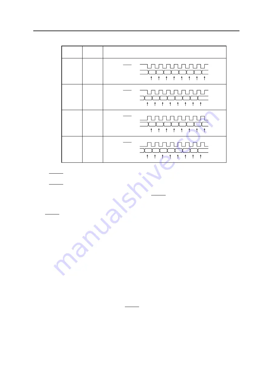
CKPn
DAPn
Specification of Data Transmission/Reception Timing in Relation to
Clock Phase
0
0
0
1
1
Note
0
1
Note
1
D7
D6
D5
D4
D3
D2
D1
D0
SCK3n (I/O)
SI3n capture
SO3n (output)
D7
D6
D5
D4
D3
D2
D1
D0
SCK3n (I/O)
SI3n capture
SO3n (output)
D7
D6
D5
D4
D3
D2
D1
D0
SCK3n (I/O)
SI3n capture
SO3n (output)
D7
D6
D5
D4
D3
D2
D1
D0
SCK3n (I/O)
SI3n capture
SO3n (output)
Summary of Contents for V850E/PH2
Page 6: ...6 Preface User s Manual U16580EE3V1UD00...
Page 16: ...16 User s Manual U16580EE3V1UD00...
Page 28: ...28 User s Manual U16580EE3V1UD00...
Page 32: ...32 User s Manual U16580EE3V1UD00...
Page 84: ...84 Chapter 2 Pin Functions User s Manual U16580EE3V1UD00 MEMO...
Page 144: ...144 Chapter 3 CPU Functions User s Manual U16580EE3V1UD00 MEMO...
Page 192: ...192 Chapter 5 Memory Access Control Function PD70F3187 only User s Manual U16580EE3V1UD00 MEMO...
Page 312: ...312 Chapter 9 16 Bit Timer Event Counter P User s Manual U16580EE3V1UD00 MEMO...
Page 534: ...534 Chapter 11 16 bit Timer Event Counter T User s Manual U16580EE3V1UD00...
Page 969: ...969 Chapter 20 Port Functions User s Manual U16580EE3V1UD00 MEMO...
Page 970: ...970 Chapter 20 Port Functions User s Manual U16580EE3V1UD00...
Page 976: ...976 Chapter 22 Internal RAM Parity Check Function User s Manual U16580EE3V1UD00 MEMO...
Page 984: ...984 Chapter 23 On Chip Debug Function OCD User s Manual U16580EE3V1UD00 MEMO...
Page 1006: ...1006 Chapter 24 Flash Memory User s Manual U16580EE3V1UD00 MEMO...
Page 1036: ...1036 Chapter 27 Recommended Soldering Conditions User s Manual U16580EE3V1UD00 MEMO...
Page 1046: ...1046 Appendix A Index User s Manual U16580EE3V1UD00 MEMO...
Page 1052: ...1052 User s Manual U16580EE3V1UD00...
Page 1053: ......


