703
Chapter 17
Clocked Serial Interface 3 (CSI3)
User’s Manual U16580EE3V1UD00
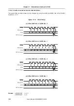
17.5.8 Transfer clock selection function
In the master mode (CKS3n2 to CKS3n0 bits of the CSIC3n register other than 111B), the bit transfer
rate can be selected by setting the CKS3n2 to CKS3n0 and MDLn2 to MDLn0 bits of the CSIC3n
register (ref. to
(2) Clocked serial interface clock select register 3n (CSIC30, CSIC31)
).
17.5.9 Single
mode
The single mode is set when the TRMDn bit of the CSIM3n register is 0 (
μ
PD70F3187: n = 0, 1,
μ
PD70F3447: n = 0).
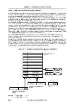
In this mode, transfer is started when the CTXEn bit or CRXEn bit is set to 1 and when data is in the
CSIBUFn register (SFEMPn bit = 0 in the SFA3n register).
If no data is in the CSIBUFn register (SFEMPn bit = 1), transfer is kept waiting until a given start
condition is satisfied.
When data is written to the CSIBUFn register while the CTXEn or CRXEn bit is 1, the CSOTn bit of the
SFA3n register (transfer status flag) is set to 1, and the chip select data (CS data) corresponding to
SIO3n load CSIBUFn pointer is transferred to the chip select output buffer. However, in slave mode
(CKS3n2 to CKS3n0 bits of the CSIC3n register = 111B) the chip select outputs (SCS3n0 to SCS3n3)
keep always the inactive level.
If transfer is not in the wait status, the transfer data indicated by the SIO3n load CSIBUFn pointer is
loaded from the CSIBUFn register to the SIO3n register, and transfer processing is started.
If the SIRB3n register is empty when one data has been transferred in the reception mode or
transmission/reception mode, the received data is stored from the SIO3n register to the SIRB3n
register, the transmission/reception completion interrupt (INTC3n) is output, and the SIO3n load
CSIBUFn pointer is incremented. If the SIRB3n register is not empty, the next transfer processing is
started. However, storing the receive data in the SIRB3n register, outputting the INTC3n interrupt, and
incrementing the SIO3n load CSIBUFn pointer are held pending, until the previously received data is
read from the SIRB3n register and the SIRB3n register becomes empty.
In the transmission mode, the INTC3n interrupt is output and the SIO3n load pointer is incremented
when transfer processing of one data has been completed (the SIRB3n register is always empty
because no data is stored from the SIO3n register to the SIRB3n register).
In all modes (transmission, reception, and transmission/reception modes), if the CSIBUFn register is
empty (write CSIBUFn pointer value = SIO3n load CSIBUFn pointer value) when transfer processing of
one data has been completed, the CSOTn bit is cleared to 0. The value of the “number of remaining
data in the CSIBUFn register (write CSIBUFn pointer – SIO3n load pointer)” can always be read from
the SFPn3 to SFPn0 bits of the SFA3n register.
Caution:
When writing data to the SFDB3n register, be sure to confirm that the SFFULn bit of
the SFA3n register is 0. Even if data is written to this register when SFFULn bit is 1,
the CSIBUFn overflow interrupt (INTC3nOVF) is output, and the written data is
ignored.
Summary of Contents for V850E/PH2
Page 6: ...6 Preface User s Manual U16580EE3V1UD00...
Page 16: ...16 User s Manual U16580EE3V1UD00...
Page 28: ...28 User s Manual U16580EE3V1UD00...
Page 32: ...32 User s Manual U16580EE3V1UD00...
Page 84: ...84 Chapter 2 Pin Functions User s Manual U16580EE3V1UD00 MEMO...
Page 144: ...144 Chapter 3 CPU Functions User s Manual U16580EE3V1UD00 MEMO...
Page 192: ...192 Chapter 5 Memory Access Control Function PD70F3187 only User s Manual U16580EE3V1UD00 MEMO...
Page 312: ...312 Chapter 9 16 Bit Timer Event Counter P User s Manual U16580EE3V1UD00 MEMO...
Page 534: ...534 Chapter 11 16 bit Timer Event Counter T User s Manual U16580EE3V1UD00...
Page 969: ...969 Chapter 20 Port Functions User s Manual U16580EE3V1UD00 MEMO...
Page 970: ...970 Chapter 20 Port Functions User s Manual U16580EE3V1UD00...
Page 976: ...976 Chapter 22 Internal RAM Parity Check Function User s Manual U16580EE3V1UD00 MEMO...
Page 984: ...984 Chapter 23 On Chip Debug Function OCD User s Manual U16580EE3V1UD00 MEMO...
Page 1006: ...1006 Chapter 24 Flash Memory User s Manual U16580EE3V1UD00 MEMO...
Page 1036: ...1036 Chapter 27 Recommended Soldering Conditions User s Manual U16580EE3V1UD00 MEMO...
Page 1046: ...1046 Appendix A Index User s Manual U16580EE3V1UD00 MEMO...
Page 1052: ...1052 User s Manual U16580EE3V1UD00...
Page 1053: ......


