968
Chapter 20
Port Functions
User’s Manual U16580EE3V1UD00
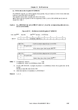
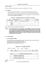
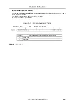
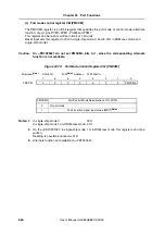
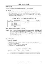
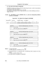
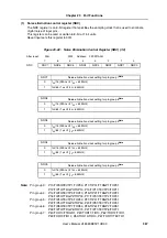
Figure 20-82:
Noise Elimination Control Register (NRC) (2/2)
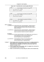
Note: Pin group 1:
(on
μ
PD70F31187) P03/INTP2/ADTRG0, P04/INTP3/ADTRG1, P30/RXDC0/INTP4,
P32/RXDC1/INTP5, P83/SCS300/INTP6, P84/SCS301/INTP7,
P85/SCS302/INTP8, P93/SCS310/INTP9, P94/SCS310/INTP10,
P95/SCS310/INTP11
(on
μ
PD70F3447)
P03/INTP2/ADTRG0, P04/INTP3/ADTRG1, P30/RXDC0/INTP4,
P32/RXDC1/INTP5, P83/SCS300/INTP6, P84/SCS301/INTP7,
P85/SCS302/INTP8, P93/INTP9, P94/INTP10,P95/INTP11
Pin group 2:
(on
μ
PD70F31187) P100/TCLR0/TICC00/TOP81, P101/TCUD0/TICC01, P102/TIUD0/TO1,
P70/TIT00/TEVTT1/TOT00, P71/TIT01/TTRGT1/TOT01,
P72/TECRT0/INTP12, P73/TIT10/TTRGT0/TOT10,
P74/TIT11/TEVTT0/TOT11, P75/TECRT1/AFO
(on
μ
PD70F3447)
P70/TIT00/TEVTT1/TOT00, P71/TIT01/TTRGT1/TOT01,
P72/TECRT0/INTP12, P73/TIT10/TTRGT0/TOT10,
P74/TIT11/TEVTT0/TOT11, P75/TECRT1/AFO
Cautions: 1. If the input pulse lasts for the duration of 4 to 5 clocks, it is undefined whether the
pulse is detected as a valid edge or eliminated as noise. So that the pulse is
actually detected as a valid edge, the same pulse level must be input for the
duration of 5 clocks or more.
2. If noise is generated in synchronization with the sampling clock, eliminate the
noise by attaching a filter to the input pin.
3. Noise is not eliminated if the corresponding pin is used as normal input port pin.
NRC2
Noise elimination clock setting for pin group 2
Note
0
f
XX
/16 (250 ns @ f
XX
= 64 MHz)
1
f
XX
/64 (1 µs @ f
XX
= 64 MHz)
NRC1
Noise elimination clock setting for pin group 1
Note
0
f
XX
/16 (250 ns @ f
XX
= 64 MHz)
1
f
XX
/64 (1 µs @ f
XX
= 64 MHz)
NRC0
Noise elimination clock setting for P00/NMI pin
0
f
XX
/16 (250 ns @ f
XX
= 64 MHz)
1
f
XX
/64 (1 µs @ f
XX
= 64 MHz)
Summary of Contents for V850E/PH2
Page 6: ...6 Preface User s Manual U16580EE3V1UD00...
Page 16: ...16 User s Manual U16580EE3V1UD00...
Page 28: ...28 User s Manual U16580EE3V1UD00...
Page 32: ...32 User s Manual U16580EE3V1UD00...
Page 84: ...84 Chapter 2 Pin Functions User s Manual U16580EE3V1UD00 MEMO...
Page 144: ...144 Chapter 3 CPU Functions User s Manual U16580EE3V1UD00 MEMO...
Page 192: ...192 Chapter 5 Memory Access Control Function PD70F3187 only User s Manual U16580EE3V1UD00 MEMO...
Page 312: ...312 Chapter 9 16 Bit Timer Event Counter P User s Manual U16580EE3V1UD00 MEMO...
Page 534: ...534 Chapter 11 16 bit Timer Event Counter T User s Manual U16580EE3V1UD00...
Page 969: ...969 Chapter 20 Port Functions User s Manual U16580EE3V1UD00 MEMO...
Page 970: ...970 Chapter 20 Port Functions User s Manual U16580EE3V1UD00...
Page 976: ...976 Chapter 22 Internal RAM Parity Check Function User s Manual U16580EE3V1UD00 MEMO...
Page 984: ...984 Chapter 23 On Chip Debug Function OCD User s Manual U16580EE3V1UD00 MEMO...
Page 1006: ...1006 Chapter 24 Flash Memory User s Manual U16580EE3V1UD00 MEMO...
Page 1036: ...1036 Chapter 27 Recommended Soldering Conditions User s Manual U16580EE3V1UD00 MEMO...
Page 1046: ...1046 Appendix A Index User s Manual U16580EE3V1UD00 MEMO...
Page 1052: ...1052 User s Manual U16580EE3V1UD00...
Page 1053: ......

