1010
Chapter 25
Electrical Specifications
User’s Manual U16580EE3V1UD00
25.3 DC
Characteristics
Unless specified otherwise, the following conditions are assumed for all characteristics in this chapter.
V
DD3x
= AV
DD
= 3.0 V to 3.6 V
V
DD1x
= CV
DD
= 1.35 V to 1.65 V
V
SS1x
= CV
SS
= V
SS3x
= AV
SSx
= 0 V
μ
PD70F3187: T
A
= -40 °C to +85 °C
μ
PD70F3187(A1): T
A
= -40 °C to +110 °C
μ
PD70F3187(A2): T
A
= -40 °C to +125 °C
Notes: 1.
Pins other than analog input pins ANI00 to ANI19
2.
Analog input pins ANI00 to ANI19
3.
No external loads considered (C
L
= 0pF). External loads cause additional pin currents. Pin
current for each pin can be calculated according to following formula:
I[µA] = 3.63
×
C
L
[pF]
×
F [MHz]
where C
L
is external load capacitance and F is the average pin toggle frequency.
Load dependent pin currents must be summed up and added to I
DD3
.
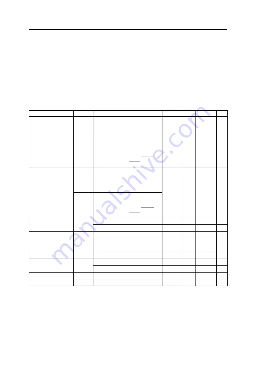
Table 25-5:
DC Characteristics
Parameter
Symbol
Conditions
MIN.
TYP.
MAX.
Unit
Input voltage, high
V
IH1
PAL0 to PAL15, PAH0 to PAH5, PDL0
to PDL15, PDH0 to PDH15, PCS0,
PCS1, PCS3, PCS4, PCD2 to PCD5,
PCT4, PCT5, PCM0, PCM1, PCM6,
PCM7, DCK, DMS, DDI, DDO
0.7 V
DD3
V
DD3
+ 0.3
V
V
IH3
P00 to P04, P10 to P17, P20 to P27,
P30 to P37, P40 to P45, P50 to P57,
P60 to P67, P70 to P75, P80 to P86,
P90 to P96, P100 to P102, RESET,
MODE0 to MODE2, DRST
Input voltage, low
V
IL1
PAL0 to PAL15, PAH0 to PAH5, PDL0
to PDL15, PDH0 to PDH15, PCS0,
PCS1, PCS3, PCS4, PCD2 to PCD5,
PCT4, PCT5, PCM0, PCM1, PCM6,
PCM7, DCK, DMS, DDI, DDO
-0.5
0.3 V
DD3
V
V
IL3
P00 to P04, P10 to P17, P20 to P27,
P30 to P37, P40 to P45, P50 to P57,
P60 to P67, P70 to P75, P80 to P86,
P90 to P96, P100 to P102, RESET,
MODE0 to MODE2, DRST
Output voltage, high
V
OH1
I
OH
= -2.5 mA
V
DD3
- 1.0
V
I
OH
= -100 µA
V
DD3
- 0.4
V
Output voltage, low
V
OL1
I
OL
= 2.5 mA
0.8
V
I
OL
= 100 µA
0.4
V
Input leakage current,
high
I
LIH
V
IH
= V
DD3
,
Note 1
10
µA
V
IH
= AV
DD
,
Note 2
3
µA
Input leakage current,
low
I
LIL
V
IL
= 0 V,
Note 1
-10
µA
V
IL
= 0 V,
Note 2
-3
µA
Power supply current
I
DD1
V
DD1
+ CV
DD
200
mA
I
DD3
V
DD3
,
Note 3
50
mA
Summary of Contents for V850E/PH2
Page 6: ...6 Preface User s Manual U16580EE3V1UD00...
Page 16: ...16 User s Manual U16580EE3V1UD00...
Page 28: ...28 User s Manual U16580EE3V1UD00...
Page 32: ...32 User s Manual U16580EE3V1UD00...
Page 84: ...84 Chapter 2 Pin Functions User s Manual U16580EE3V1UD00 MEMO...
Page 144: ...144 Chapter 3 CPU Functions User s Manual U16580EE3V1UD00 MEMO...
Page 192: ...192 Chapter 5 Memory Access Control Function PD70F3187 only User s Manual U16580EE3V1UD00 MEMO...
Page 312: ...312 Chapter 9 16 Bit Timer Event Counter P User s Manual U16580EE3V1UD00 MEMO...
Page 534: ...534 Chapter 11 16 bit Timer Event Counter T User s Manual U16580EE3V1UD00...
Page 969: ...969 Chapter 20 Port Functions User s Manual U16580EE3V1UD00 MEMO...
Page 970: ...970 Chapter 20 Port Functions User s Manual U16580EE3V1UD00...
Page 976: ...976 Chapter 22 Internal RAM Parity Check Function User s Manual U16580EE3V1UD00 MEMO...
Page 984: ...984 Chapter 23 On Chip Debug Function OCD User s Manual U16580EE3V1UD00 MEMO...
Page 1006: ...1006 Chapter 24 Flash Memory User s Manual U16580EE3V1UD00 MEMO...
Page 1036: ...1036 Chapter 27 Recommended Soldering Conditions User s Manual U16580EE3V1UD00 MEMO...
Page 1046: ...1046 Appendix A Index User s Manual U16580EE3V1UD00 MEMO...
Page 1052: ...1052 User s Manual U16580EE3V1UD00...
Page 1053: ......


