217
Chapter 6
DMA Functions (DMA Controller)
User’s Manual U16580EE3V1UD00
6.5 DMA Interrupt Function
The peripheral I/O interrupts of the A/D converters and the serial interfaces, which serve as DMA
trigger factors, are shared with the DMA transfer completion interrupt of the corresponding channel n
(INTDMAn) (n = 0, 1, 4 to 7). When a DMA channel is enabled the specified peripheral I/O interrupt is
no longer applied to the interrupt controller. Instead of it the corresponding DMA transfer completion
interrupt is applied to the appropriate interrupt handler address.
In opposite to the other interrupts serving as DMA trigger factors, the TMR0 interrupts INTTR0OD and
INTTR0CD, and the TMR1 interrupts INTTR1OD and INTTR1CD respectively, are not shared with DMA
transfer completion interrupt of channel 2 (INTDMA2) and channel 3 (INTDMA3) respectively. These
DMA completion interrupts have dedicated entries in the interrupt source list (refer to
”Interrupt/Exception Source List” on page 219
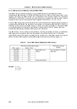
Table 6-4 shows the relations between DMA trigger factors and DMA completion interrupts.
Notes: 1.
Not available on
μ
PD70F3447.
2.
An interrupt request is not generated for a signal, which serves as DMA trigger factor.
Instead of this the defined DMA completion interrupt request is executed on the same inter-
rupt entry address of the DMA trigger factor.
Table 6-4:
Relations Between DMA Trigger Factors and DMA Completion Interrupts
DMA channel
DMA trigger factor
DMA completion interrupt
Remark
Name
Entry
Handler
Address
0
INTAD0
INTDMA0
INTAD0
00000670H
Note 2
1
INTAD1
INTDMA1
INTAD1
00000680H
Note 2
2
INTTR0CD or
INTR0OD
INTDMA2
INTDMA2
000006F0H
3
INTTR1CD or
INTR1OD
INTDMA3
INTDMA3
00000700H
4, 5
INTC30
INTDMA4,
INTDMA5
INTC30
000005E0H
Note 2
INTC31
Note 1
INTC31
Note 1
00000600H
Note 2
INTCB0R
INTCB0R
00000580H
Note 2
INTCB1R
Note 1
INTCB1R
Note 1
000005B0H
Note 2
INTUC0R
INTUC0R
00000620H
Note 2
INTUC1R
INTUC1R
00000650H
Note 2
6, 7
INTC30
INTDMA6,
INTDMA7
INTC30
000005E0H
Note 2
INTC31
Note 1
INTC31
Note 1
00000600H
Note 2
INTCB0T
INTCB0T
00000570H
Note 2
INTCB1T
Note 1
INTCIB1T
Note 1
000005A0H
Note 2
INTUC0T
INTUC0T
00000630H
Note 2
INTUC1T
INTUC1T
00000660H
Note 2
Summary of Contents for V850E/PH2
Page 6: ...6 Preface User s Manual U16580EE3V1UD00...
Page 16: ...16 User s Manual U16580EE3V1UD00...
Page 28: ...28 User s Manual U16580EE3V1UD00...
Page 32: ...32 User s Manual U16580EE3V1UD00...
Page 84: ...84 Chapter 2 Pin Functions User s Manual U16580EE3V1UD00 MEMO...
Page 144: ...144 Chapter 3 CPU Functions User s Manual U16580EE3V1UD00 MEMO...
Page 192: ...192 Chapter 5 Memory Access Control Function PD70F3187 only User s Manual U16580EE3V1UD00 MEMO...
Page 312: ...312 Chapter 9 16 Bit Timer Event Counter P User s Manual U16580EE3V1UD00 MEMO...
Page 534: ...534 Chapter 11 16 bit Timer Event Counter T User s Manual U16580EE3V1UD00...
Page 969: ...969 Chapter 20 Port Functions User s Manual U16580EE3V1UD00 MEMO...
Page 970: ...970 Chapter 20 Port Functions User s Manual U16580EE3V1UD00...
Page 976: ...976 Chapter 22 Internal RAM Parity Check Function User s Manual U16580EE3V1UD00 MEMO...
Page 984: ...984 Chapter 23 On Chip Debug Function OCD User s Manual U16580EE3V1UD00 MEMO...
Page 1006: ...1006 Chapter 24 Flash Memory User s Manual U16580EE3V1UD00 MEMO...
Page 1036: ...1036 Chapter 27 Recommended Soldering Conditions User s Manual U16580EE3V1UD00 MEMO...
Page 1046: ...1046 Appendix A Index User s Manual U16580EE3V1UD00 MEMO...
Page 1052: ...1052 User s Manual U16580EE3V1UD00...
Page 1053: ......


