558
Chapter 12
16-bit 2-Phase Encoder Input Up/Down Counter/General Purpose Timer (TMENC10)
User’s Manual U16580EE3V1UD00
12.5.3 Operation in UDC mode
(1)
Overview of operation in UDC mode
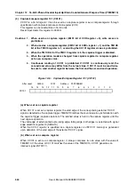
The count clock input to TMENC10 in the UDC mode (CMD bit of TUM10 register = 1) can only be
externally input from the TIUD1 and TCUD1 pins. Up/down count judgment in the UDC mode is
determined based on the phase difference of the TIUD1 and TCUD1 pin inputs according to the
PRM10 register setting (there is a total of four choices).
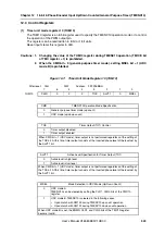
The UDC mode is further divided into two modes according to the TMENC10 clear conditions (count
operation is performed only with TIUD1, TCUD1 input in both modes).
•
UDC mode A (TUM register’s CMD bit = 1, MSEL bit = 0)
The TMENC10 clear source can be selected as only external clear input (TCLR1), a match signal
between the TMENC10 count value and the CM100 set value during up count operation, or logical
sum (OR) of the two signals, using bits CLR1 and CLR0 of the TMC10 register.
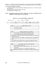
TMENC10 can transfer (reload) the value of CM100 upon occurrence of TMENC10 underflow,
when the RLEN bit of the TMC10 register is set (1).
•
UDC mode B (TUMn register’s CMD bit = 1, MSEL bit = 1)
The status of TMENC10 after match of the TMENC10 count value and CM100 set value is as
follows.
<1> In case of an up count operation, TMENC10 is cleared (0000H), and the INTCM10 interrupt
is generated.
<2> In case of a down count operation, the TMENC10 count value is decremented (-1).
The status of TMENC10 after match of the TMENC10 count value and CM101 set value is as
follows.
<1> In case of an up count operation, the TMENC10 count value is incremented (+1).
<2> In case of a down count operation, TMENC10 is cleared (0000H), and the INTCM11
interrupt is generated.
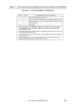
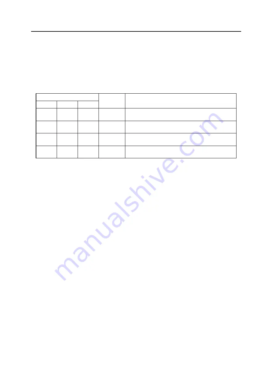
Table 12-4:
List of Count Operations in UDC Mode
PRM10 Register
Operation
Mode
TM1n Operation
PRM102
PRM101
PRM100
1
0
0
Mode 1
Down count when TCUD1 = high level
Up count when TCUD1 = low level
1
0
1
Mode 2
Up count upon detection of valid edge of TIUD1 input
Down count upon detection of valid edge of TCUD1 input
1
1
0
Mode 3
Automatic judgment in TCUD1 input level upon detection
of valid edge of TIUD1 input
1
1
1
Mode 4
Automatic judgment upon detection of both edges of
TIUD1 input and both edges of TCUD1 input
Summary of Contents for V850E/PH2
Page 6: ...6 Preface User s Manual U16580EE3V1UD00...
Page 16: ...16 User s Manual U16580EE3V1UD00...
Page 28: ...28 User s Manual U16580EE3V1UD00...
Page 32: ...32 User s Manual U16580EE3V1UD00...
Page 84: ...84 Chapter 2 Pin Functions User s Manual U16580EE3V1UD00 MEMO...
Page 144: ...144 Chapter 3 CPU Functions User s Manual U16580EE3V1UD00 MEMO...
Page 192: ...192 Chapter 5 Memory Access Control Function PD70F3187 only User s Manual U16580EE3V1UD00 MEMO...
Page 312: ...312 Chapter 9 16 Bit Timer Event Counter P User s Manual U16580EE3V1UD00 MEMO...
Page 534: ...534 Chapter 11 16 bit Timer Event Counter T User s Manual U16580EE3V1UD00...
Page 969: ...969 Chapter 20 Port Functions User s Manual U16580EE3V1UD00 MEMO...
Page 970: ...970 Chapter 20 Port Functions User s Manual U16580EE3V1UD00...
Page 976: ...976 Chapter 22 Internal RAM Parity Check Function User s Manual U16580EE3V1UD00 MEMO...
Page 984: ...984 Chapter 23 On Chip Debug Function OCD User s Manual U16580EE3V1UD00 MEMO...
Page 1006: ...1006 Chapter 24 Flash Memory User s Manual U16580EE3V1UD00 MEMO...
Page 1036: ...1036 Chapter 27 Recommended Soldering Conditions User s Manual U16580EE3V1UD00 MEMO...
Page 1046: ...1046 Appendix A Index User s Manual U16580EE3V1UD00 MEMO...
Page 1052: ...1052 User s Manual U16580EE3V1UD00...
Page 1053: ......

