612
Chapter 15
Asynchronous Serial Interface C (UARTC)
User’s Manual U16580EE3V1UD00
15.3 Control
Registers
(1)
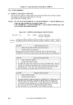
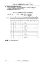
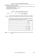
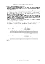
UARTCn control register 0 (UCnCTL0)
The UCnCTL0 register is an 8-bit register that controls the UARTCn serial transfer operation.
This register can be read or written in 8-bit or 1-bit units.
Reset input sets this register to 10H.
Caution:
Be sure to set the UCnPWR bit = 1 and the UCnRXE bit = 1 while the RXDCn pin is
high level (when UCnRDL bit of UCnOP0 register = 0).
If the UCnPWR bit = 1 and the UCnRXE bit = 1 are set while the RXDCn pin is low
level, reception will inadvertently start.
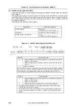
Figure 15-2:
UARTCn Control Register 0 (UCnCTL0) (1/2)
After reset:
10H
R/W
Address:
UC0CTL0 FFFFFA00H,
UC1CTL0 FFFFFA20H
7
6
5
4
3
2
1
0
UCnCTL0
UCnPWR UCnTXE
UCnRXE
UCnDIR
UCnPS1
UCnPS0
UCnCL
UCnSL
(n = 0, 1)
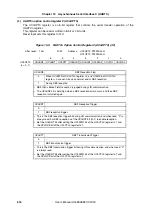
UCnPWR
UARTCn Operation Control
0
Stops clock operation (UARTCn reset asynchronously)
1
Enables operating clock operation
Operating clock control and UARTCn asynchronous reset are performed with the
UCnPWR bit. The TXDCn pin output is fixed to high level by setting the UCnPWR bit to 0.
UCnTXE
Transmission Operation Enable
0
Stops transmission operation
1
Enables transmission operation
•
The TXDCn pin output is fixed to high level by setting the UCnPWR bit to 0. Since the
UCnTXE bit is initialized by the operating clock, to initialize the transmission unit, set
UCnTXE from 0 to 1, and 2 clocks later, the transmission enabled status is entered.
•
When UCnPWR bit = 0, the value written to the UCnTXE bit is ignored.
UCnRXE
Reception Operation Enable
0
Stops reception operation
1
Enables reception operation
•
The receive operation is stopped by setting the UCnRXE bit to 0. Therefore, even if the
prescribed data is transferred, no reception completion interrupt is output and the
UARTCn reception data register (UCnRX) is not updated. Since the UCnRXE bit is
synchronized using the operating clock, to initialize the reception unit, set UCnRXE
from 0 to 1, and 2 clocks later, the reception enabled status is entered.
•
When UCnPWR bit = 0, the value written to the UCnRXE bit is ignored.
Summary of Contents for V850E/PH2
Page 6: ...6 Preface User s Manual U16580EE3V1UD00...
Page 16: ...16 User s Manual U16580EE3V1UD00...
Page 28: ...28 User s Manual U16580EE3V1UD00...
Page 32: ...32 User s Manual U16580EE3V1UD00...
Page 84: ...84 Chapter 2 Pin Functions User s Manual U16580EE3V1UD00 MEMO...
Page 144: ...144 Chapter 3 CPU Functions User s Manual U16580EE3V1UD00 MEMO...
Page 192: ...192 Chapter 5 Memory Access Control Function PD70F3187 only User s Manual U16580EE3V1UD00 MEMO...
Page 312: ...312 Chapter 9 16 Bit Timer Event Counter P User s Manual U16580EE3V1UD00 MEMO...
Page 534: ...534 Chapter 11 16 bit Timer Event Counter T User s Manual U16580EE3V1UD00...
Page 969: ...969 Chapter 20 Port Functions User s Manual U16580EE3V1UD00 MEMO...
Page 970: ...970 Chapter 20 Port Functions User s Manual U16580EE3V1UD00...
Page 976: ...976 Chapter 22 Internal RAM Parity Check Function User s Manual U16580EE3V1UD00 MEMO...
Page 984: ...984 Chapter 23 On Chip Debug Function OCD User s Manual U16580EE3V1UD00 MEMO...
Page 1006: ...1006 Chapter 24 Flash Memory User s Manual U16580EE3V1UD00 MEMO...
Page 1036: ...1036 Chapter 27 Recommended Soldering Conditions User s Manual U16580EE3V1UD00 MEMO...
Page 1046: ...1046 Appendix A Index User s Manual U16580EE3V1UD00 MEMO...
Page 1052: ...1052 User s Manual U16580EE3V1UD00...
Page 1053: ......

