696
Chapter 17
Clocked Serial Interface 3 (CSI3)
User’s Manual U16580EE3V1UD00
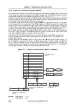
17.5.2 Function of CSI data buffer register (CSIBUFn)
By consecutively writing the transmit data to the SFCS3n register and the SFDB3n register from where
it is transferred, the data can be stored in the CSIBUFn register while the CSIBUFn pointer for writing is
automatically incremented (the CSIBUFn register size is 20 bits × 16) (n = 0, 1).
When the chip select outputs SCS3n0 to SCS3n3 are used, write SFCS3n register before the SFDB3n
register. However, in slave mode the chip select outputs SCS3n0 to SCSS3n3 keep the inactive level
and therefore writing to the SFCS3n register is not necessary.
The condition under which transfer is to be started (SFEMPn bit of the SFA3n register = 0) is satisfied
when data is written to the lower 8 bits of the SFDB3n register (or SFDB3nL register). If a transfer data
length of 9 bits or more is specified (CCLn3 to CCLn0 bits of the CSIL3n register = 0000B, or 1001B to
1111B), data must be written to the SFDB3n register in 16-bit units or to the SFDB3nH and SFDB3nL
registers, in that order, in 8-bit units. If the transfer data length is set to 8 bits (CCLn3 to CCLn0
bits = 1000B), data must be written to the SFDB3nL register in 8-bit units or to the SFDB3n register in
16-bit units. If data is written to the SFDB3nL register in 16-bit units, however, the higher 8 bits of the
data (of the SFDB3nH register) are ignored and not transferred.
The SFFULn bit of the SFA3n register is set to 1 when 16 data exist in the CSIBUFn register and
outputs a CSIBUFn overflow interrupt (INTC3nOVF) when the SFFULn bit = 1 and when the 17th
transfer data is written.
Sixteen data exist in the CSIBUFn register in the single mode (TRMDn bit of the CSIM3n register = 0)
when “CSIBUFn pointer value for writing = CSIBUFn pointer value for SIO3n loading, and SFFULn
bit = 1”. When the CSIBUFn pointer for SIO3n loading is incremented after completion of transfer, the
CSIBUFn register has a vacancy of one data (in the consecutive mode (TRMDn bit = 1), the CSIBUFn
register does not have a vacancy even if one data has been transferred).
Figure 17-11:
Function of CSI Data Buffer Register n (CSIBUFn)
Remark:
μ
PD70F3187:
n = 0, 1
μ
PD70F3447:
n = 0
CSI data buffer register n
(CSIBUFn)
15
16
19
15
0
0
Transfer data 0
CS data 0
CS data 1
CS data 2
CS data 3
CS data 4
Transfer data 1
Transfer data 2
Transfer data 3
Transfer data 4
SFPn3 to
SFPn0
7
0
3
4
3
4
CSIBUF status register
3n (SFA3n)
Incremented
SIO3n load
CSIBUFn pointer
Incremented
Write
CSIBUFn pointer
Transmit data CSI buffer register 3n
(SFDB3n)
SFDB3nH
SFDB3nL
15
8 7
0
Chip select CSI buffer register 3n
(SFCS3n)
15
8 7
0
SFCS3n3 to
SFCS3n0
Summary of Contents for V850E/PH2
Page 6: ...6 Preface User s Manual U16580EE3V1UD00...
Page 16: ...16 User s Manual U16580EE3V1UD00...
Page 28: ...28 User s Manual U16580EE3V1UD00...
Page 32: ...32 User s Manual U16580EE3V1UD00...
Page 84: ...84 Chapter 2 Pin Functions User s Manual U16580EE3V1UD00 MEMO...
Page 144: ...144 Chapter 3 CPU Functions User s Manual U16580EE3V1UD00 MEMO...
Page 192: ...192 Chapter 5 Memory Access Control Function PD70F3187 only User s Manual U16580EE3V1UD00 MEMO...
Page 312: ...312 Chapter 9 16 Bit Timer Event Counter P User s Manual U16580EE3V1UD00 MEMO...
Page 534: ...534 Chapter 11 16 bit Timer Event Counter T User s Manual U16580EE3V1UD00...
Page 969: ...969 Chapter 20 Port Functions User s Manual U16580EE3V1UD00 MEMO...
Page 970: ...970 Chapter 20 Port Functions User s Manual U16580EE3V1UD00...
Page 976: ...976 Chapter 22 Internal RAM Parity Check Function User s Manual U16580EE3V1UD00 MEMO...
Page 984: ...984 Chapter 23 On Chip Debug Function OCD User s Manual U16580EE3V1UD00 MEMO...
Page 1006: ...1006 Chapter 24 Flash Memory User s Manual U16580EE3V1UD00 MEMO...
Page 1036: ...1036 Chapter 27 Recommended Soldering Conditions User s Manual U16580EE3V1UD00 MEMO...
Page 1046: ...1046 Appendix A Index User s Manual U16580EE3V1UD00 MEMO...
Page 1052: ...1052 User s Manual U16580EE3V1UD00...
Page 1053: ......


