709
Chapter 17
Clocked Serial Interface 3 (CSI3)
User’s Manual U16580EE3V1UD00
17.5.15 Transfer
wait
function
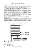
In the master mode (CKS3n2 to CKS3n0 bits of the CSIC3n register other than 111B), starting transfer
can be delayed by one clock, depending on the setting of the CSWEn bit of the CSIM3n register
(CSWEn bit = 1). The CSWEn bit is valid only in the master mode. In the slave mode (CKS3n2 to
CKS3n0 bits = 111B), setting the CSWEn bit to 1 is prohibited (even if set, transfer wait is not inserted).
When the transfer wait function is enabled (CSWEn bit = 1), the chip select outputs can be
During transfer wait (CSWE bit = 1) the chip select outputs (SCS3n0 to SCS3n3) can be configured for
an intermediate inactive level output of half a clock period by setting the CSMDn bit of the CSIM3n
register to 1.
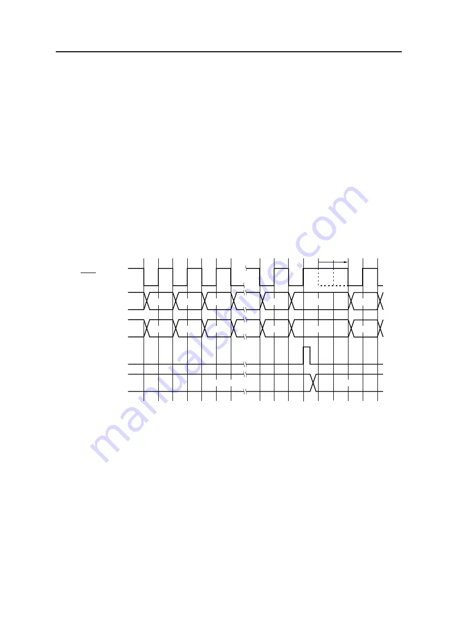
Figure 17-21:
Transfer Wait Function (1/3)
(a) Transfer Wait Enabled (CSWEn Bit = 1),
INTC3n Delay Disabled (CSITn Bit = 0),
CKPn and DAPn Bits = 00B,
Transfer Data Length: 8 Bits (CCLn3 to CCLn0 bits = 1000B)
Intermediate Inactive Chip Select Level Disabled (CSMDn = 0)
Remark:
μ
PD70F3187:
n = 0, 1
μ
PD70F3447:
n = 0
DI7
DI6
DI5
DO7
CS data
CS data
DO6
DO5
SCK3n (output)
SI3n (input)
SO3n (output)
INTC3n interrupt
SCS3n0 to
SCS3n3 (outputs)
DI7
DI1
DI0
Wait
DO1
DO0
DO7
Summary of Contents for V850E/PH2
Page 6: ...6 Preface User s Manual U16580EE3V1UD00...
Page 16: ...16 User s Manual U16580EE3V1UD00...
Page 28: ...28 User s Manual U16580EE3V1UD00...
Page 32: ...32 User s Manual U16580EE3V1UD00...
Page 84: ...84 Chapter 2 Pin Functions User s Manual U16580EE3V1UD00 MEMO...
Page 144: ...144 Chapter 3 CPU Functions User s Manual U16580EE3V1UD00 MEMO...
Page 192: ...192 Chapter 5 Memory Access Control Function PD70F3187 only User s Manual U16580EE3V1UD00 MEMO...
Page 312: ...312 Chapter 9 16 Bit Timer Event Counter P User s Manual U16580EE3V1UD00 MEMO...
Page 534: ...534 Chapter 11 16 bit Timer Event Counter T User s Manual U16580EE3V1UD00...
Page 969: ...969 Chapter 20 Port Functions User s Manual U16580EE3V1UD00 MEMO...
Page 970: ...970 Chapter 20 Port Functions User s Manual U16580EE3V1UD00...
Page 976: ...976 Chapter 22 Internal RAM Parity Check Function User s Manual U16580EE3V1UD00 MEMO...
Page 984: ...984 Chapter 23 On Chip Debug Function OCD User s Manual U16580EE3V1UD00 MEMO...
Page 1006: ...1006 Chapter 24 Flash Memory User s Manual U16580EE3V1UD00 MEMO...
Page 1036: ...1036 Chapter 27 Recommended Soldering Conditions User s Manual U16580EE3V1UD00 MEMO...
Page 1046: ...1046 Appendix A Index User s Manual U16580EE3V1UD00 MEMO...
Page 1052: ...1052 User s Manual U16580EE3V1UD00...
Page 1053: ......

