Data Port Interface Protocol
92
•
SPACELBS interfaces the N-595 with a SpaceLabs monitor
•
MARQ interfaces the N-595 with a GE Marquette monitor
•
DATEX interfaces the N-595 with a Datex-Ohmeda AS/3 monitor
Note:
Selecting AGILEN, SPACELBS, MARQ, or DATEX automatically
sets the baud rate to the rate applicable for that protocol.
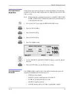
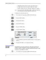
To change the communication protocol:
1. Turn on the N-595 by pressing the POWER ON/OFF button.
2. Press the SETUP softkey.
3. Press the NEXT softkey.
4. Press the NEXT softkey.
5. Press the COMM softkey.
6. Press the SELECT softkey.
7. Use the ADJUST UP and ADJUST DOWN buttons to select the desired
protocol.
8. Press the EXIT softkey to save the protocol setting.
Language
Selection
Eight languages can be viewed on the screen and sent to the printer. The
languages are ENGLISH, FRANCAIS (French), DEUTSCH (German),
ITALIANO (Italian), ESPANOL (Spanish), NEDERLANDS (Dutch), PORT
(Portuguese), and SVERIGE (Swedish).
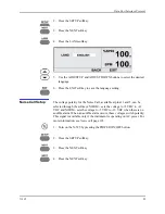
1. Turn on the N-595 by pressing the POWER ON/OFF button.
Summary of Contents for OXIMAX N-595
Page 1: ......
Page 8: ...This page intentionally left blank...
Page 13: ...Introduction N 595 5 Figure 4 Trend Softkey Map...
Page 50: ...This page intentionally left blank...
Page 76: ...This page intentionally left blank...
Page 82: ...This page intentionally left blank...
Page 96: ...This page intentionally left blank...
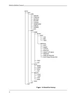
Page 98: ...Data Port Interface Protocol 90 Figure 19 Data Port Setup...
Page 116: ...This page intentionally left blank...
Page 125: ...Figure 27 Main PCB Schematic Diagram Sheet 1 of 13 117...
Page 126: ...Figure 28 Main PCB Schematic Diagram Sheet 2 of 13 119...
Page 127: ...Figure 29 Main PCB Schematic Diagram Sheet 3 of 13 121...
Page 128: ...Figure 30 Main PCB Schematic Diagram Sheet 4 of 13 123...
Page 129: ...Figure 31 Main PCB Schematic Diagram Sheet 5 of 13 125...
Page 130: ...Figure 32 Main PCB Schematic Diagram Sheet 6 of 13 127...
Page 131: ...Figure 33 Main PCB Schematic Diagram Sheet 7 of 13 129...
Page 132: ...Figure 34 Main PCB Schematic Diagram Sheet 8 of 13 131...
Page 133: ...Figure 35 Main PCB Schematic Diagram Sheet 9 of 13 133...
Page 134: ...Figure 36 Main PCB Schematic Diagram Sheet 10 of 13 135...
Page 135: ...Figure 37 Main PCB Schematic Diagram Sheet 11 of 13 137...
Page 136: ...Figure 38 Main PCB Schematic Diagram Sheet 12 of 13 139...
Page 137: ...Figure 39 Main PCB Schematic Diagram Sheet 13 of 13 141...
Page 138: ...Figure 40 Main PCB Assembly Drawing Front View 143...
Page 141: ...Figure 43 Linear Power Supply Assembly Drawing 149 AC FERRITE DC FERRITE...


