Data Port Interface Protocol
N-595
103
Patient Data and
Operating Status
Time
The Time column represents the N-595 real-time clock.
Patient Data
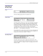
Patient data and the operating status of the unit are highlighted in the display
above. Parameter values, at the time of the printout, are displayed directly
beneath the heading for each parameter. In this example the %SpO
2
is 100,
and the pulse rate (BPM) is 190 beats per minute. The asterisk (*) next to the
190 indicates that 190 beats per minute is outside of the alarm limits,
indicated in the top row, for pulse rate. If no data for a parameter is available,
three dashes (- - -) will be displayed in the printout.
Pulse Amplitude (PA) can range from 0 to 254. There are no alarm parameters
for this value. It can be used for trending information and is an indication of a
change in pulse volume, pulse strength, or circulation.
Operating Status
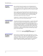
The Status column indicates alarm conditions and operating status of the
N-595. In this example the PH means Pulse High. The status codes are listed
in Table 19 on page 104. As many as 4 codes can be displayed at one time in
the Status column.
Summary of Contents for OXIMAX N-595
Page 1: ......
Page 8: ...This page intentionally left blank...
Page 13: ...Introduction N 595 5 Figure 4 Trend Softkey Map...
Page 50: ...This page intentionally left blank...
Page 76: ...This page intentionally left blank...
Page 82: ...This page intentionally left blank...
Page 96: ...This page intentionally left blank...
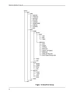
Page 98: ...Data Port Interface Protocol 90 Figure 19 Data Port Setup...
Page 116: ...This page intentionally left blank...
Page 125: ...Figure 27 Main PCB Schematic Diagram Sheet 1 of 13 117...
Page 126: ...Figure 28 Main PCB Schematic Diagram Sheet 2 of 13 119...
Page 127: ...Figure 29 Main PCB Schematic Diagram Sheet 3 of 13 121...
Page 128: ...Figure 30 Main PCB Schematic Diagram Sheet 4 of 13 123...
Page 129: ...Figure 31 Main PCB Schematic Diagram Sheet 5 of 13 125...
Page 130: ...Figure 32 Main PCB Schematic Diagram Sheet 6 of 13 127...
Page 131: ...Figure 33 Main PCB Schematic Diagram Sheet 7 of 13 129...
Page 132: ...Figure 34 Main PCB Schematic Diagram Sheet 8 of 13 131...
Page 133: ...Figure 35 Main PCB Schematic Diagram Sheet 9 of 13 133...
Page 134: ...Figure 36 Main PCB Schematic Diagram Sheet 10 of 13 135...
Page 135: ...Figure 37 Main PCB Schematic Diagram Sheet 11 of 13 137...
Page 136: ...Figure 38 Main PCB Schematic Diagram Sheet 12 of 13 139...
Page 137: ...Figure 39 Main PCB Schematic Diagram Sheet 13 of 13 141...
Page 138: ...Figure 40 Main PCB Assembly Drawing Front View 143...
Page 141: ...Figure 43 Linear Power Supply Assembly Drawing 149 AC FERRITE DC FERRITE...


