Performance Verification
12
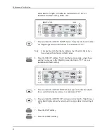
alarm limit for %SpO
2
will indicate an alarm limit of “100” (or
institutional default setting) inside a box.
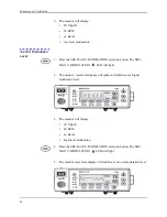
3. Press and hold the ADJUST DOWN button. Verify that the boxed number
for %SpO
2
upper alarm limit reduces to a minimum of “86.”
Note:
A decimal point in the display indicates that the alarm limits have
been changed from factory default values.
4. Press the SELECT softkey. Verify that the monitor emits a single beep
and the box moves to the %SpO
2
lower alarm limit of “85” (or your
institutional default setting).
5. Press and hold the ADJUST DOWN button and verify that the %SpO
2
lower alarm limit display reduces to a minimum of “20.”
6. Press and hold the ADJUST UP button and verify that the %SpO
2
lower
alarm limit display cannot be raised past the upper alarm limit setting of
“85.”
7. Press the EXIT softkey.
8. Press the LIMITS softkey
Summary of Contents for OXIMAX N-595
Page 1: ......
Page 8: ...This page intentionally left blank...
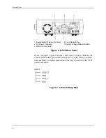
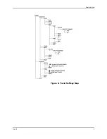
Page 13: ...Introduction N 595 5 Figure 4 Trend Softkey Map...
Page 50: ...This page intentionally left blank...
Page 76: ...This page intentionally left blank...
Page 82: ...This page intentionally left blank...
Page 96: ...This page intentionally left blank...
Page 98: ...Data Port Interface Protocol 90 Figure 19 Data Port Setup...
Page 116: ...This page intentionally left blank...
Page 125: ...Figure 27 Main PCB Schematic Diagram Sheet 1 of 13 117...
Page 126: ...Figure 28 Main PCB Schematic Diagram Sheet 2 of 13 119...
Page 127: ...Figure 29 Main PCB Schematic Diagram Sheet 3 of 13 121...
Page 128: ...Figure 30 Main PCB Schematic Diagram Sheet 4 of 13 123...
Page 129: ...Figure 31 Main PCB Schematic Diagram Sheet 5 of 13 125...
Page 130: ...Figure 32 Main PCB Schematic Diagram Sheet 6 of 13 127...
Page 131: ...Figure 33 Main PCB Schematic Diagram Sheet 7 of 13 129...
Page 132: ...Figure 34 Main PCB Schematic Diagram Sheet 8 of 13 131...
Page 133: ...Figure 35 Main PCB Schematic Diagram Sheet 9 of 13 133...
Page 134: ...Figure 36 Main PCB Schematic Diagram Sheet 10 of 13 135...
Page 135: ...Figure 37 Main PCB Schematic Diagram Sheet 11 of 13 137...
Page 136: ...Figure 38 Main PCB Schematic Diagram Sheet 12 of 13 139...
Page 137: ...Figure 39 Main PCB Schematic Diagram Sheet 13 of 13 141...
Page 138: ...Figure 40 Main PCB Assembly Drawing Front View 143...
Page 141: ...Figure 43 Linear Power Supply Assembly Drawing 149 AC FERRITE DC FERRITE...


