Performance Verification
16
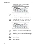
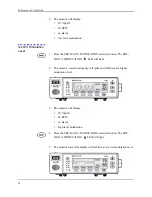
9. Press the ADJUST UP button until the SpO
2
lower alarm limit indicates
99.
10. Press the SELECT softkey three times to select pulse rate lower alarm
limit.
11. Press the ADJUST UP button until the pulse rate lower alarm limit
indicates 160.
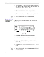
12. Verify the following monitor reactions:
•
The plethysmograph waveform tracks your pulse rate.
•
The pulse tone is heard.
•
Your SpO
2
and pulse rate are flashing in the %SpO
2
and BPM
displays.
•
The audible alarm sounds indicating that both parameters have
violated the alarm limits.
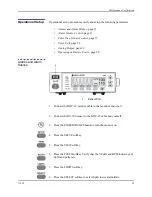
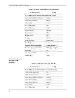
13. Press and hold the ALARM SILENCE button until the the BPM display
indicates “SEC.” Continue to press the ALARM SILENCE button and
press the ADJUST DOWN button until “60” is displayed in the %SPO2
display.
14. Press the ALARM SILENCE button.
15. With the monitor’s alarm silenced, verify the following:
•
The alarm remains silenced for 60 seconds.
•
The ALARM SILENCE indicator lights.
•
The %SpO
2
and BPM displays continue to flash.
•
The pulse tone is still audible.
•
The audible alarm returns in approximately 60 seconds.
16. Press and hold the ALARM SILENCE button until the the BPM display
indicates “SEC.” Continue to press the ALARM SILENCE button and
press the ADJUST DOWN button until “30” is displayed in the %SPO2
display.
17. Press the ADJUST UP button and verify that the displays indicate
60 SEC, 90 SEC, 120 SEC, and OFF. Release the ADJUST UP button
when the display indicates “OFF.”
Summary of Contents for OXIMAX N-595
Page 1: ......
Page 8: ...This page intentionally left blank...
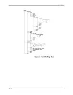
Page 13: ...Introduction N 595 5 Figure 4 Trend Softkey Map...
Page 50: ...This page intentionally left blank...
Page 76: ...This page intentionally left blank...
Page 82: ...This page intentionally left blank...
Page 96: ...This page intentionally left blank...
Page 98: ...Data Port Interface Protocol 90 Figure 19 Data Port Setup...
Page 116: ...This page intentionally left blank...
Page 125: ...Figure 27 Main PCB Schematic Diagram Sheet 1 of 13 117...
Page 126: ...Figure 28 Main PCB Schematic Diagram Sheet 2 of 13 119...
Page 127: ...Figure 29 Main PCB Schematic Diagram Sheet 3 of 13 121...
Page 128: ...Figure 30 Main PCB Schematic Diagram Sheet 4 of 13 123...
Page 129: ...Figure 31 Main PCB Schematic Diagram Sheet 5 of 13 125...
Page 130: ...Figure 32 Main PCB Schematic Diagram Sheet 6 of 13 127...
Page 131: ...Figure 33 Main PCB Schematic Diagram Sheet 7 of 13 129...
Page 132: ...Figure 34 Main PCB Schematic Diagram Sheet 8 of 13 131...
Page 133: ...Figure 35 Main PCB Schematic Diagram Sheet 9 of 13 133...
Page 134: ...Figure 36 Main PCB Schematic Diagram Sheet 10 of 13 135...
Page 135: ...Figure 37 Main PCB Schematic Diagram Sheet 11 of 13 137...
Page 136: ...Figure 38 Main PCB Schematic Diagram Sheet 12 of 13 139...
Page 137: ...Figure 39 Main PCB Schematic Diagram Sheet 13 of 13 141...
Page 138: ...Figure 40 Main PCB Assembly Drawing Front View 143...
Page 141: ...Figure 43 Linear Power Supply Assembly Drawing 149 AC FERRITE DC FERRITE...

