Performance Verification
18
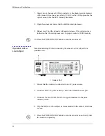
3. Press the ADJUST UP button to return the beep volume to a comfortable
level.
4. Remove the sensor from your finger. Disconnect the DOC-10 monitor
cable and the sensor.
Nurse Call
1.
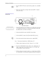
Data Port Connector
1. Connect the negative lead of a voltmeter to pin 5 and positive lead to pin
11 of the data port connector (1) on the back of the monitor. Ensure that
the audible alarm is not silenced or turned off.
2. Connect the SRC-MAX tester to the DOC-10 sensor cable.
3. Connect the DOC-10 sensor cable to the monitor SpO
2
connector.
4. Turn on the monitor and wait for the monitor to complete POST.
Note:
The monitor should indicate a %SPO2 alarm of 75.
5. Verify an output voltage at pins 5 and 11 b5 to +12 VDC.
6. Press the ALARM SILENCE button. With no active audible alarm, the
output voltage at pins 5 and 11 must be between -5 to -12 VDC. This
verifies the RS-232 Nurse Call function.
7. With the instrument in an alarm condition, use a digital voltmeter (DVM)
to verify that there is no continuity (1 megohms or greater) between pins 8
Summary of Contents for OXIMAX N-595
Page 1: ......
Page 8: ...This page intentionally left blank...
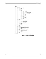
Page 13: ...Introduction N 595 5 Figure 4 Trend Softkey Map...
Page 50: ...This page intentionally left blank...
Page 76: ...This page intentionally left blank...
Page 82: ...This page intentionally left blank...
Page 96: ...This page intentionally left blank...
Page 98: ...Data Port Interface Protocol 90 Figure 19 Data Port Setup...
Page 116: ...This page intentionally left blank...
Page 125: ...Figure 27 Main PCB Schematic Diagram Sheet 1 of 13 117...
Page 126: ...Figure 28 Main PCB Schematic Diagram Sheet 2 of 13 119...
Page 127: ...Figure 29 Main PCB Schematic Diagram Sheet 3 of 13 121...
Page 128: ...Figure 30 Main PCB Schematic Diagram Sheet 4 of 13 123...
Page 129: ...Figure 31 Main PCB Schematic Diagram Sheet 5 of 13 125...
Page 130: ...Figure 32 Main PCB Schematic Diagram Sheet 6 of 13 127...
Page 131: ...Figure 33 Main PCB Schematic Diagram Sheet 7 of 13 129...
Page 132: ...Figure 34 Main PCB Schematic Diagram Sheet 8 of 13 131...
Page 133: ...Figure 35 Main PCB Schematic Diagram Sheet 9 of 13 133...
Page 134: ...Figure 36 Main PCB Schematic Diagram Sheet 10 of 13 135...
Page 135: ...Figure 37 Main PCB Schematic Diagram Sheet 11 of 13 137...
Page 136: ...Figure 38 Main PCB Schematic Diagram Sheet 12 of 13 139...
Page 137: ...Figure 39 Main PCB Schematic Diagram Sheet 13 of 13 141...
Page 138: ...Figure 40 Main PCB Assembly Drawing Front View 143...
Page 141: ...Figure 43 Linear Power Supply Assembly Drawing 149 AC FERRITE DC FERRITE...

