Specifications
80
Manufacturer’s
Declaration
WARNING: The use of accessories, transducers, and cables other than
those specified may result in increased emission and/or decreased
immunity of the N-595 pulse oximeter.
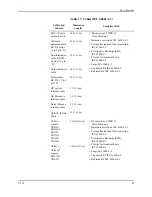
Electrical fast transient/burst
immunity
IEC 61000-4-4, level 3
Item
Compliant With
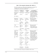
Table 13: Electromagnetic Emissions (IEC 60601-1-2)
The N-595 is suitable for use in the specified electromagnetic environment. The
customer and/or user of the N-595 should assure that it is used in an
electromagnetic environment as described below:
Emissions Test
Compliance
Electromagnetic Environment
Guidance
RF emission
CISPR 11
Class B/
Group 1
The N-595 must emit electromagnetic
energy in order to perform its intended
function. Nearby electronic equipment
may be affected.
RF emissions
CISPR 11
Class B/
Group 1
The N-595 is suitable for use in all
establishments.
Harmonic emissions
IEC 61000-3-2
Complies
Voltage fluctuations/
flicker emission
IEC 61000-3-3
Complies
Summary of Contents for OXIMAX N-595
Page 1: ......
Page 8: ...This page intentionally left blank...
Page 13: ...Introduction N 595 5 Figure 4 Trend Softkey Map...
Page 50: ...This page intentionally left blank...
Page 76: ...This page intentionally left blank...
Page 82: ...This page intentionally left blank...
Page 96: ...This page intentionally left blank...
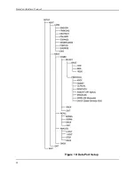
Page 98: ...Data Port Interface Protocol 90 Figure 19 Data Port Setup...
Page 116: ...This page intentionally left blank...
Page 125: ...Figure 27 Main PCB Schematic Diagram Sheet 1 of 13 117...
Page 126: ...Figure 28 Main PCB Schematic Diagram Sheet 2 of 13 119...
Page 127: ...Figure 29 Main PCB Schematic Diagram Sheet 3 of 13 121...
Page 128: ...Figure 30 Main PCB Schematic Diagram Sheet 4 of 13 123...
Page 129: ...Figure 31 Main PCB Schematic Diagram Sheet 5 of 13 125...
Page 130: ...Figure 32 Main PCB Schematic Diagram Sheet 6 of 13 127...
Page 131: ...Figure 33 Main PCB Schematic Diagram Sheet 7 of 13 129...
Page 132: ...Figure 34 Main PCB Schematic Diagram Sheet 8 of 13 131...
Page 133: ...Figure 35 Main PCB Schematic Diagram Sheet 9 of 13 133...
Page 134: ...Figure 36 Main PCB Schematic Diagram Sheet 10 of 13 135...
Page 135: ...Figure 37 Main PCB Schematic Diagram Sheet 11 of 13 137...
Page 136: ...Figure 38 Main PCB Schematic Diagram Sheet 12 of 13 139...
Page 137: ...Figure 39 Main PCB Schematic Diagram Sheet 13 of 13 141...
Page 138: ...Figure 40 Main PCB Assembly Drawing Front View 143...
Page 141: ...Figure 43 Linear Power Supply Assembly Drawing 149 AC FERRITE DC FERRITE...

