N-595
1
I n t r o d u c t i o n
Warnings
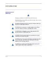
Warnings are identified by the WARNING symbol shown above.
Warnings alert the user to potential serious outcomes (death, injury, or adverse
events) to the patient or user.
WARNING: Explosion hazard. Do not use the N-595 pulse oximeter in
the presence of flammable anesthetics.
WARNING: Do not spray, pour, or spill any liquid on the N-595, its
accessories, connectors, switches, or openings in the chassis.
WARNING: Before attempting to open or disassemble the N-595,
disconnect the power cord from the N-595.
WARNING: The LCD panel contains toxic chemicals. Do not ingest
chemicals from a broken LCD panel.
WARNING: The use of accessories, transducers, and cables other than
those specified may result in increased emission and/or decreased
immunity of the N-595 pulse oximeter.
WARNING: Do not silence the N-595 audible alarm or decrease its
volume if patient safety could be compromised.
Summary of Contents for OXIMAX N-595
Page 1: ......
Page 8: ...This page intentionally left blank...
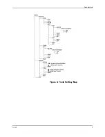
Page 13: ...Introduction N 595 5 Figure 4 Trend Softkey Map...
Page 50: ...This page intentionally left blank...
Page 76: ...This page intentionally left blank...
Page 82: ...This page intentionally left blank...
Page 96: ...This page intentionally left blank...
Page 98: ...Data Port Interface Protocol 90 Figure 19 Data Port Setup...
Page 116: ...This page intentionally left blank...
Page 125: ...Figure 27 Main PCB Schematic Diagram Sheet 1 of 13 117...
Page 126: ...Figure 28 Main PCB Schematic Diagram Sheet 2 of 13 119...
Page 127: ...Figure 29 Main PCB Schematic Diagram Sheet 3 of 13 121...
Page 128: ...Figure 30 Main PCB Schematic Diagram Sheet 4 of 13 123...
Page 129: ...Figure 31 Main PCB Schematic Diagram Sheet 5 of 13 125...
Page 130: ...Figure 32 Main PCB Schematic Diagram Sheet 6 of 13 127...
Page 131: ...Figure 33 Main PCB Schematic Diagram Sheet 7 of 13 129...
Page 132: ...Figure 34 Main PCB Schematic Diagram Sheet 8 of 13 131...
Page 133: ...Figure 35 Main PCB Schematic Diagram Sheet 9 of 13 133...
Page 134: ...Figure 36 Main PCB Schematic Diagram Sheet 10 of 13 135...
Page 135: ...Figure 37 Main PCB Schematic Diagram Sheet 11 of 13 137...
Page 136: ...Figure 38 Main PCB Schematic Diagram Sheet 12 of 13 139...
Page 137: ...Figure 39 Main PCB Schematic Diagram Sheet 13 of 13 141...
Page 138: ...Figure 40 Main PCB Assembly Drawing Front View 143...
Page 141: ...Figure 43 Linear Power Supply Assembly Drawing 149 AC FERRITE DC FERRITE...

