Specifications
84
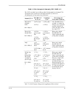
Table 16: Recommended Separation Distances
Recommended Separation Distances between Portable and Mobile RF
Communications Equipment and the N-595 (IEC 60601-1-2)
Frequency of
Transmitter
150 kHz to
80 MHz
80 MHz to
800 MHz
800 MHz to
2.5 GHz
Equation
d
= 1.2
√
P
d
= 1.2
√
P
d
= 2.3
√
P
Rated Maximum
Output Power of
Transmitter in
Watts
Separation
Distance in
Meters
Separation
Distance in
Meters
Separation
Distance in
Meters
0.01
0.12
0.12
0.23
0.1
0.38
0.38
0.73
1
1.2
1.2
2.3
10
3.8
3.8
7.3
100
12
12
23
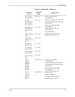
For transmitters rated at a maximum output power not listed above, the separation
distance can be estimated using the equation in the corresponding column, where
P
is the maximum output [power rating of the transmitter in watts (W)] according
to the transmitter manufacturer.
Note: These guidelines may not apply in all situations. Electromagnetic
propagation is affected by absorption and reflection from structures, objects,
and people.
Summary of Contents for OXIMAX N-595
Page 1: ......
Page 8: ...This page intentionally left blank...
Page 13: ...Introduction N 595 5 Figure 4 Trend Softkey Map...
Page 50: ...This page intentionally left blank...
Page 76: ...This page intentionally left blank...
Page 82: ...This page intentionally left blank...
Page 96: ...This page intentionally left blank...
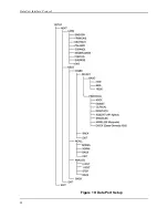
Page 98: ...Data Port Interface Protocol 90 Figure 19 Data Port Setup...
Page 116: ...This page intentionally left blank...
Page 125: ...Figure 27 Main PCB Schematic Diagram Sheet 1 of 13 117...
Page 126: ...Figure 28 Main PCB Schematic Diagram Sheet 2 of 13 119...
Page 127: ...Figure 29 Main PCB Schematic Diagram Sheet 3 of 13 121...
Page 128: ...Figure 30 Main PCB Schematic Diagram Sheet 4 of 13 123...
Page 129: ...Figure 31 Main PCB Schematic Diagram Sheet 5 of 13 125...
Page 130: ...Figure 32 Main PCB Schematic Diagram Sheet 6 of 13 127...
Page 131: ...Figure 33 Main PCB Schematic Diagram Sheet 7 of 13 129...
Page 132: ...Figure 34 Main PCB Schematic Diagram Sheet 8 of 13 131...
Page 133: ...Figure 35 Main PCB Schematic Diagram Sheet 9 of 13 133...
Page 134: ...Figure 36 Main PCB Schematic Diagram Sheet 10 of 13 135...
Page 135: ...Figure 37 Main PCB Schematic Diagram Sheet 11 of 13 137...
Page 136: ...Figure 38 Main PCB Schematic Diagram Sheet 12 of 13 139...
Page 137: ...Figure 39 Main PCB Schematic Diagram Sheet 13 of 13 141...
Page 138: ...Figure 40 Main PCB Assembly Drawing Front View 143...
Page 141: ...Figure 43 Linear Power Supply Assembly Drawing 149 AC FERRITE DC FERRITE...

