Data Port Interface Protocol
N-595
91
Communication
Baud Rate
The baud rate may need to be changed to match the abilities of the attached
equipment. Perform the following procedure to change the baud rate to 2400,
9600, or 19200.
Note:
When setting the communication protocol to AGILENT, SPACELBS,
MARQ, or DATEX the communication baud rate is automatically set
to the applicable baud rate.
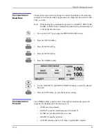
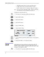
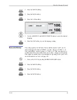
1. Turn on the N-595 by pressing the POWER ON/OFF button.
2. Press the SETUP softkey.
3. Press the NEXT softkey.
4. Press the NEXT softkey.
5. Press the COMM softkey.
6. Use the ADJUST UP and ADJUST DOWN buttons to select the desired
baud rate.
7. Press the EXIT softkey to save the baud rate setting.
Communication
Protocol
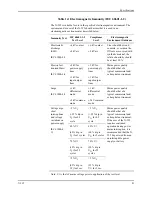
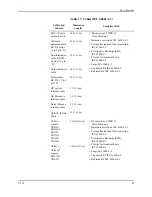
The COMM softkey is used to select from eight communication protocols
supported by the data port. The selections are:
•
ASCII used for printouts
•
OXINET to enable communication with Oxinet II
•
CLINICAL intended for Nellcor use only
•
GRAPH for graphic printouts
•
AGILEN interfaces the N-595 with an Agilent (HP) monitor
Summary of Contents for OXIMAX N-595
Page 1: ......
Page 8: ...This page intentionally left blank...
Page 13: ...Introduction N 595 5 Figure 4 Trend Softkey Map...
Page 50: ...This page intentionally left blank...
Page 76: ...This page intentionally left blank...
Page 82: ...This page intentionally left blank...
Page 96: ...This page intentionally left blank...
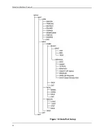
Page 98: ...Data Port Interface Protocol 90 Figure 19 Data Port Setup...
Page 116: ...This page intentionally left blank...
Page 125: ...Figure 27 Main PCB Schematic Diagram Sheet 1 of 13 117...
Page 126: ...Figure 28 Main PCB Schematic Diagram Sheet 2 of 13 119...
Page 127: ...Figure 29 Main PCB Schematic Diagram Sheet 3 of 13 121...
Page 128: ...Figure 30 Main PCB Schematic Diagram Sheet 4 of 13 123...
Page 129: ...Figure 31 Main PCB Schematic Diagram Sheet 5 of 13 125...
Page 130: ...Figure 32 Main PCB Schematic Diagram Sheet 6 of 13 127...
Page 131: ...Figure 33 Main PCB Schematic Diagram Sheet 7 of 13 129...
Page 132: ...Figure 34 Main PCB Schematic Diagram Sheet 8 of 13 131...
Page 133: ...Figure 35 Main PCB Schematic Diagram Sheet 9 of 13 133...
Page 134: ...Figure 36 Main PCB Schematic Diagram Sheet 10 of 13 135...
Page 135: ...Figure 37 Main PCB Schematic Diagram Sheet 11 of 13 137...
Page 136: ...Figure 38 Main PCB Schematic Diagram Sheet 12 of 13 139...
Page 137: ...Figure 39 Main PCB Schematic Diagram Sheet 13 of 13 141...
Page 138: ...Figure 40 Main PCB Assembly Drawing Front View 143...
Page 141: ...Figure 43 Linear Power Supply Assembly Drawing 149 AC FERRITE DC FERRITE...


