background image

Chapter 5  BIOS 

68 

Chapter 5 

BIOS 


5.1  Introduction 


The BIOS is programmed onto the BIOS chip.  The BIOS setup program 

allows changes to certain system settings.  This chapter outlines the options 

that can be changed. 


NOTE: 


Some of the BIOS options may vary throughout the life cycle of the 

product and are subject to change without prior notice.


5.1.1 

Starting Setup 


The UEFI BIOS is activated when the computer is turned on.  The setup 

program can be activated in one of two ways. 

1.  Press the 

DEL 

or 

F2 

key as soon as the system is turned on or 

2.  Press the 

DEL 

or 

F2 

key when the “

Press DEL or F2 to enter SETUP

” 

message appears on the screen. 

If the message disappears before the 

DEL or F2 

key is pressed, restart the 

computer and try again. 


5.1.2 

Using Setup 

Use the arrow keys to highlight items, press 

ENTER 

to select, use the 

PageUp and PageDown keys to change entries, press 

F1 

for help and press 

ESC 

to quit.  Navigation keys are shown in. 


Key


Function


Up arrow 

Move to previous item 

Down arrow  Move to next item 

Left arrow 

Move to the item on the left hand side 

Right arrow 

Move to the item on the right hand side 

Increase the numeric value or make changes 

Decrease the numeric value or make changes 

Page Up key  Increase the numeric value or make changes 

Summary of Contents for AESQ67-967

Page 1: ...AESQ67 967 Single Board Computer Full Size PICMG 1 3 CPU Card supports Intel Q67 Chipset User s Manual Rev 2 01 Date September 12 2014 ...

Page 2: ...tors 22 3 1 1 AESQ67 967 Series Layout 22 3 1 2 Peripheral Interface Connectors 22 3 1 3 External Interface Panel Connectors 23 3 2 Internal Peripheral Connectors 23 3 2 1 12V Power Connector 23 3 2 2 Audio Kit Connector 24 3 2 3 Battery Connector 25 3 2 4 DDR3 DIMM Slots 26 3 2 5 Digital I O Connector 27 3 2 6 DVI D Connector DVI Model Only 27 3 2 7 Fan Connector CPU 28 3 2 8 Front Panel Connecto...

Page 3: ... Clear CMOS Jumper 54 4 3 3 Wake on LAN Jumper 55 4 4 Chassis Installation 56 4 4 1 Airflow 56 4 4 2 CPU Card Installation 56 4 5 Internal Peripheral Device Connections 57 4 5 1 Dual RS 232 Cable with Slot Bracket 57 4 5 2 DVI D USB Kit Installation DVI Model Only 58 4 5 3 SATA Drive Connection 59 4 5 4 USB Cable Dual Port with Slot Bracket 60 4 5 5 PCIe Mini Card Installation 62 4 6 External Peri...

Page 4: ...5 4 1 Northbridge Configuration 87 5 4 2 Southbridge Configuration 89 5 4 3 Integrated Graphics 92 5 4 4 ME Subsystem 93 5 5 Boot 94 5 6 Security 95 5 7 Exit 96 Appendix A BIOS Options 97 Appendix B Terminology 99 Appendix C Digital I O Interface 102 C 1 Introduction 102 C 2 Assembly Language Sample 1 102 C 3 Assembly Language Sample 2 103 Appendix D Watchdog Timer 104 Appendix E Intel Matrix Stor...

Page 5: ...oard Mouse Connector Location 33 Figure 3 13 Parallel Port Connector Location 34 Figure 3 14 PCIe Mini Card Slot Location 35 Figure 3 15 SATA 3Gb s Drive Connector Location 36 Figure 3 16 SATA 6Gb s Drive Connector Location 37 Figure 3 17 Serial Port Connector Location 38 Figure 3 18 RS 422 485 Connector Location 39 Figure 3 19 SMBus Connector Location 40 Figure 3 20 SPI Connector Location 41 Figu...

Page 6: ...Cable Installation 57 Figure 4 11 DVI D USB Kit Installation 58 Figure 4 12 SATA Drive Cable Connection 59 Figure 4 13 SATA Power Drive Connection 60 Figure 4 14 Dual USB Cable Connection 62 Figure 4 15 PCIe Mini Card Installation 63 Figure 4 16 LAN Connection 64 Figure 4 17 USB Device Connection 65 Figure 4 18 VGA Connector 66 ...

Page 7: ...eyboard Mouse Connector Pinouts 33 Table 3 13 Parallel Port Connector Pinouts 34 Table 3 14 PCIe Mini Card Slot Pinouts 36 Table 3 15 SATA 3Gb s Drive Connector Pinouts 37 Table 3 16 SATA 6Gb s Drive Connector Pinouts 38 Table 3 17 Serial Port Connector Pinouts 38 Table 3 18 RS 422 485Connector Pinouts 39 Table 3 19 DB 9 RS 422 485 Pinouts 39 Table 3 20 SMBus Connector Pinouts 40 Table 3 21 SPI Co...

Page 8: ...Preface 7 Table D 1 AH 6FH Sub function 104 ...

Page 9: ...8 BIOS Menu 10 Super IO Configuration 79 BIOS Menu 11 Serial Port n Configuration Menu 80 BIOS Menu 12 Parallel Port Configuration Menu 82 BIOS Menu 13 H W Monitor 84 BIOS Menu 14 FAN 1 Configuration 85 BIOS Menu 15 Serial Port Console Redirection 86 BIOS Menu 16 Chipset 87 BIOS Menu 17 Northbridge Chipset Configuration 88 BIOS Menu 18 Southbridge Chipset Configuration 90 BIOS Menu 19 Integrated G...

Page 10: ... Copyright Notice The information in this document is subject to change without prior notice in order to improve reliability design and function and does not represent a commitment on the part of the manufacturer In no event will the manufacturer be liable for direct indirect special incidental or consequential damages arising out of the use or inability to use the product or documentation even if...

Page 11: ...Preface 10 Trademarks All registered trademarks and product names mentioned herein are used for identification purposes only and may be trademarks and or registered trademarks of their respective owners ...

Page 12: ...dules up to 16 0 GB The AESQ67 967 Series supports two GbE interfaces through the Intel 82579 Ethernet PHY with Intel AMT 7 0 support and the Intel 82583V Ethernet controller The integrated Intel Q67 chipset supports two SATA 6Gb s and four SATA 3Gb s drives Two USB 2 0 on the rear panel six USB 2 0 by pin header and one PCIe Mini interface provide flexible expansion options High Definition Audio ...

Page 13: ...of the AESQ67 967 Series motherboard features are listed below PICMG 1 3 full size graphics grade solution LGA1155 CPU socket Intel Q67 chipset Dual channel DDR3 DIMMs support up to 16 0 GB Dual independent display by VGA and DVI D DVI model only One PCIe Mini expansion slot Two Intel PCIe Gigabit Ethernet connectors LAN2 with Intel AMT 7 0 support Two SATA 6Gb s connectors with RAID function Four...

Page 14: ...Chapter 1 Introduction 13 1 4 Connectors The connectors on the AESQ67 967 Series are shown in the figure below Figure 1 2 Connectors ...

Page 15: ...Chapter 1 Introduction 14 1 5 Dimensions The main dimensions of the AESQ67 967 Series are shown in the diagram below Figure 1 3 AESQ67 967 Series Dimensions mm ...

Page 16: ...Chapter 1 Introduction 15 Figure 1 4 External Interface Panel Dimensions mm ...

Page 17: ...w Figure 1 5 shows the data flow between the system chipset the CPU and other components installed on the motherboard Figure 1 5 Data Flow Diagram 1 7 Technical Specifications The AESQ67 967 Series technical specifications are listed below ...

Page 18: ...ogrammable supports 1 255 sec system reset Expansion One PCIe Mini slot with USB 2 0 1 1 signal PCIe signal and PCI signal via golden fingers Supports PCIex1 or x4 slots on backplane I O Interface Connectors Audio Connector One internal audio connector 10 pin header Digital I O 8 bit 4 bit input 4 bit output Display Output One VGA integrated in the Intel Q67 rear I O One DVI D integrated in the In...

Page 19: ...pin header USB Ports Two external USB 2 0 ports on rear IO Six internal USB 2 0 ports by three pin headers Environmental and Power Specifications Power Supply 5V 12V AT ATX power supported Power Consumption 3 3V 1 69A 5V 3 45A 12V 0 32A Vcore 5 24A 5VSb 0 17 3 40 GHz Intel Core i7 2600 CPU with two 1333 MHz 2GB DDR3 memory Operating Temperature 10 60 Storage Temperature 20 70 Humidity 5 95 non con...

Page 20: ...nti static pad When configuring any circuit board place it on an anti static mat Only handle the edges of the PCB Don t touch the surface of the motherboard Hold the motherboard by the edges when handling 2 2 Unpacking Precautions When the AESQ67 967 Series is unpacked please do the following Follow the antistatic guidelines above Make sure the packing box is facing upwards when opening Make sure ...

Page 21: ...ntity Item and Part Number Image 1 AESQ67 967 Series CPU card 4 SATA cable P N 32000 062800 RS 1 Dual RS 232 cable P N 19800 000051 RS 1 Dual USB cable with bracket P N 19800 003100 300 RS 1 Mini jumper pack 1 DVI D USB kit DVI model only P N IO KIT 001 R20 1 Utility CD Table 2 1 Packing List ...

Page 22: ...RS 422 485 cable 200 mm P N 32205 003800 300 RS KB MS cable with bracket P N 19800 000075 RS SATA to IDE CF converter board P N SAIDE KIT01 R10 SATA power cable P N 32102 000100 200 RS LPT cable P N 19800 000049 RS 7 1 channel HD audio kit with Realtek ALC892 audio codec supporting dual audio stream P N AC KIT 892HD R10 Table 2 2 Optional Items ...

Page 23: ...l Interface Connectors The table below lists all the connectors on the board Connector Type Label 12V ATX power supply connector 4 pin Molex power connector CPU12V1 Audio kit connector 10 pin header J_AUDIO1 Battery connector 2 pin wafer BT2 DDR3 DIMM sockets 240 pin socket CHA_DIMM1 CHB_DIMM1 Digital I O connector 10 pin header DIO1 DVI D connector DVI model only 26 pin header DVI1 Fan connector ...

Page 24: ... header COM1 COM2 COM3 COM4 SMBus connector 4 pin wafer SMBUS_1 SPI ROM connector 8 pin header JSPI1 TPM connector 20 pin header TPM1 USB connectors 8 pin header USB1 USB2 USB3 Table 3 1 Peripheral Interface Connectors 3 1 3 External Interface Panel Connectors The table below lists the connectors on the external I O panel Connector Type Label Ethernet connector RJ 45 LAN1 Ethernet connector RJ 45 ...

Page 25: ...tor supports the 12V power supply Figure 3 2 ATX Power Connector Pinout Location Pin Description Pin Description 1 GND 2 GND 3 12V 4 12V Table 3 3 ATX Power Connector Pinouts 3 2 2 Audio Kit Connector CN Label J_AUDIO1 CN Type 10 pin header CN Location See Figure 3 3 CN Pinouts See Table 3 4 This connector connects to an external audio kit ...

Page 26: ...3 2 3 Battery Connector CAUTION Risk of explosion if battery is replaced by an incorrect type Only certified engineers should replace the on board battery Dispose of used batteries according to instructions and local regulations CN Label BAT1 CN Type 2 pin wafer CN Location See Figure 3 4 CN Pinouts See Table 3 5 This is connected to the system battery The battery provides power to the system cloc...

Page 27: ...ation Pin Description 1 GND 2 Battery Table 3 5 Battery Connector Pinouts 3 2 4 DDR3 DIMM Slots CN Label CHA_DIMM1 CHB_DIMM1 CN Type DDR3 DIMM slot CN Location See Figure 3 5 The DIMM slots are for DDR3 DIMM memory modules Figure 3 5 DDR3 DIMM Slot Locations ...

Page 28: ...xternal devices The digital I O provides 4 bit output and 4 bit input Figure 3 6 Digital I O Connector Location PIN NO DESCRIPTION PIN NO DESCRIPTION 1 GND 2 VCC 3 Output 3 4 Output 2 5 Output 1 6 Output 0 7 Input 3 8 Input 2 9 Input 1 10 Input 0 Table 3 6 Digital I O Connector Pinouts 3 2 6 DVI D Connector DVI Model Only CN Label DVI1 CN Type 26 pin header CN Location See Figure 3 7 CN Pinouts Se...

Page 29: ...Connector Location Pin Description Pin Description 1 Data 2 2 Data 2 3 GND 4 NC 5 NC 6 DDC Clock 7 DDC Data 8 NC 9 Data 1 10 Data 1 11 GND 12 NC 13 NC 14 VCC 15 GND 16 Hot Plug Detect 17 Data 0 18 Data 0 19 GND 20 NC 21 NC 22 GND 23 Clock 24 Clock 25 GND 26 NC Table 3 7 DVI D Connector Pinouts 3 2 7 Fan Connector CPU CN Label CPU_FAN1 ...

Page 30: ...8 CPU Fan Connector Location PIN NO DESCRIPTION 1 GND 2 12 V 3 Rotation Signal 4 PWM Control Signal Table 3 8 CPU Fan Connector Pinouts 3 2 8 Front Panel Connector CN Label F_PANEL1 CN Type 14 pin header CN Location See Figure 3 9 CN Pinouts See Table 3 9 The front panel connector connects to the indicator LEDs and buttons on the computer s front panel ...

Page 31: ...5V Speaker 2 5V 3 N C 4 N C 5 GROUND 6 N C Power Button 7 PWR_BTN 8 Speaker 9 PWR_BTN Reset 10 N C HDD LED 11 5V 12 RESET 13 HDD_LED 14 GROUND Table 3 9 Front Panel Connector Pinouts 3 2 9 I2 C Connector CN Label I2C_1 CN Type 4 pin wafer CN Location See Figure 3 10 CN Pinouts See Table 3 10 The I2C connector is for system debug ...

Page 32: ...GND 2 PCH_GP38_PU 3 PCH_GP39_PU 4 5VS Table 3 10 I2C Connector Pinouts 3 2 10 Infrared Interface Connector CN Label IR1 CN Type 5 pin header CN Location See Figure 3 11 CN Pinouts See Table 3 11 The infrared connector attaches to an infrared receiver for use with remote controls ...

Page 33: ...C 3 IR RX 4 GND 5 IR TX Table 3 11 Infrared Connector Pinouts 3 2 11 Keyboard Mouse Connector CN Label KB_MS1 CN Type 6 pin wafer CN Location See Figure 3 12 CN Pinouts See Table 3 12 The keyboard mouse connector connects to a PS 2 Y cable that can be connected to a PS 2 keyboard and mouse ...

Page 34: ...rd Data 5 Keyboard Clock 6 GROUND Table 3 12 Keyboard Mouse Connector Pinouts 3 2 12 Parallel Port Connector CN Label LPT1 CN Type 26 pin box header CN Location See Figure 3 13 CN Pinouts See Table 3 13 The parallel port connector connects to a parallel port connector interface or some other parallel port device such as a printer ...

Page 35: ...A5 8 DATA6 9 DATA7 10 ACKNOWLEDGE 11 BUSY 12 PAPER EMPTY 13 PRINTER SELECT 14 AUTO FORM FEED 15 ERROR 16 INITIALIZE 17 PRINTER SELECT LN 18 GND 19 GND 20 GND 21 GND 22 GND 23 GND 24 GND 25 GND Table 3 13 Parallel Port Connector Pinouts 3 2 13 PCIe Mini Card Slot CN Label CN3 CN Type PCIe Mini card slot CN Location See Figure 3 14 CN Pinouts See Table 3 14 ...

Page 36: ...ption Pin Description 1 PCIE_WAKE 2 VCC3 3 NC 4 GND 5 NC 6 1 5V 7 CLKREQ 8 LFRAME 9 GND 10 LAD3 11 CLK 12 LAD2 13 CLK 14 LAD1 15 GND 16 LAD0 17 PCIRST 18 GND 19 LPC 20 VCC3 21 GND 22 PCIRST 23 PERN2 24 3VDual 25 PERP2 26 GND 27 GND 28 1 5V 29 GND 30 SMBCLK 31 PETN2 32 SMBDATA 33 PETP2 34 GND 35 GND 36 USBD 37 NC 38 USBD 39 NC 40 GND 41 NC 42 NC ...

Page 37: ...lot Pinouts 3 2 14 SATA 3Gb s Drive Connector CN Label SATA3 SATA4 SATA5 SATA6 CN Type 7 pin SATA drive connector CN Location See Figure 3 15 CN Pinouts See Table 3 15 The SATA drive connectors can be connected to SATA drives and support up to 3Gb s data transfer rate Figure 3 15 SATA 3Gb s Drive Connector Location Pin Description Pin Description 1 GND 2 TX ...

Page 38: ...Gb s Drive Connector CN Label SATA1 SATA2 CN Type 7 pin SATA drive connector CN Location See Figure 3 16 CN Pinouts See Table 3 16 The SATA drive connectors can be connected to SATA drives and support up to 6Gb s data transfer rate Figure 3 16 SATA 6Gb s Drive Connector Location Pin Description Pin Description 1 GND 2 TX 3 TX 4 GND 5 RX 6 RX ...

Page 39: ... of these connectors provides RS 232 connections Figure 3 17 Serial Port Connector Location Pin Description Pin Description 1 Data Carrier Direct DCD 2 Receive Data RXD 3 Transmit Data TXD 4 Data Terminal Ready DTR 5 Ground GND 6 Data Set Ready DSR 7 Request To Send RTS 8 Clear To Send CTS 9 Ring Indicator RI 10 N C Table 3 17 Serial Port Connector Pinouts 3 2 17 Serial Port Connector RS 422 485 C...

Page 40: ... Location PIN NO DESCRIPTION PIN NO DESCRIPTION 1 RXD422 3 TXD422 TXD485 2 RXD422 4 TXD422 TXD485 Table 3 18 RS 422 485Connector Pinouts Use the optional RS 422 485 cable to connect to a serial device The pinouts of the DB 9 connector are listed below RS 422 Pinouts RS 485 Pinouts Table 3 19 DB 9 RS 422 485 Pinouts 3 2 18 SMBus Connector ...

Page 41: ...Bus System Management Bus connector provides low speed system management communications Figure 3 19 SMBus Connector Location Pin Description 1 GND 2 SMB_DATA 3 SMB_CLK 4 V5S Table 3 20 SMBus Connector Pinouts 3 2 19 SPI ROM Connector CN Label JSPI1 CN Type 8 pin header CN Location See Figure 3 20 CN Pinouts See Table 3 21 ...

Page 42: ...Location PIN NO DESCRIPTION PIN NO DESCRIPTION 1 3 3V 2 GND 3 SPI_CS0 4 SPI_CLK 5 SPI_SO0 6 SPI_SI 7 NC 8 NC Table 3 21 SPI Connector Pinouts 3 2 20 TPM Connector CN Label TPM1 CN Type 20 pin header CN Location See Figure 3 21 CN Pinouts See Table 3 22 The TPM connector connects to a TPM module ...

Page 43: ...AD2 9 3V 10 AD1 11 AD0 12 GND 13 SMB_CLK 14 SMB_DATA 15 SB3V 16 SERIRQ 17 GND 18 CLKRUN 19 PM_SUS_STAT 20 DRQ Table 3 22 TPM Connector Pinouts 3 2 21 USB Connectors CN Label USB1 USB2 USB3 CN Type 8 pin header CN Location See Figure 3 22 CN Pinouts See Table 3 23 The USB connectors connect to USB devices Each pin header provides two USB ports ...

Page 44: ...ort Connector Pinouts 3 3 External Peripheral Interface Connector Panel The figure below shows the external peripheral interface connector EPIC panel The EPIC panel consists of the following Figure 3 23 External Peripheral Interface Connector 3 3 1 Ethernet Connectors CN Label LAN1 and LAN2 CN Type RJ 45 CN Location See Figure 3 23 CN Pinouts See Figure 3 24 and Table 3 24 ...

Page 45: ...DIA0 Table 3 24 LAN Pinouts Figure 3 24 Ethernet Connector LED Description LED Description A on linked blinking data is being sent received B off 10 Mb s green 100 Mb s orange 1000 Mb s Table 3 25 Connector LEDs 3 3 2 USB Connectors CN Label USB_C1 and USB_C2 CN Type USB port CN Location See Figure 3 23 CN Pinouts See Table 3 26 The AESQ67 967 Series has two external USB 2 0 ports The ports connec...

Page 46: ...N Location See Figure 3 23 CN Pinouts See Figure 3 25 and Table 3 27 The VGA connector connects to a monitor that accepts a standard VGA input Pin Description Pin Description 1 RED 2 GREEN 3 BLUE 4 NC 5 GND 6 GND 7 GND 8 GND 9 VGAVCC 10 GND 11 NC 12 DDCDAT 13 HSYNC 14 VSYNC 15 DDCCLK Table 3 27 VGA Connector Pinouts Figure 3 25 VGA Connector ...

Page 47: ...nti static wristband can help to prevent ESD from damaging the board Self grounding Before handling the board touch any grounded conducting material During the time the board is handled frequently touch any conducting materials that are connected to the ground Use an anti static pad When configuring the AESQ67 967 Series place it on an antic static pad This reduces the possibility of ESD damaging ...

Page 48: ...otential ESD damage Turn all power to the AESQ67 967 Series off When working with the AESQ67 967 Series make sure that it is disconnected from all power supplies and that no electricity is being fed into the system Before and during the installation of the AESQ67 967 Series DO NOT Remove any of the stickers on the PCB board These stickers are required for warranty validation Use the product before...

Page 49: ...e lever See Figure 4 1 Figure 4 1 Disengage the CPU Socket Load Lever Step 2 Open the socket and remove the protective cover The black protective cover can be removed by pulling up on the tab labeled Remove See Figure 4 2 Figure 4 2 Remove Protective Cover Step 3 Inspect the CPU socket Make sure there are no bent pins and make sure the socket contacts are free of foreign material If any ...

Page 50: ...wo orientation notches on the CPU with the socket alignment keys Step 7 Insert the CPU Gently insert the CPU into the socket If the CPU pins are properly aligned the CPU should slide into the CPU socket smoothly See Figure 4 3 Figure 4 3 Insert the Socket LGA1155 CPU Step 8 Close the CPU socket Close the load plate and pull the load lever back a little to have the load plate be able to secure to t...

Page 51: ...tion The cooling kit has a heatsink and fan WARNING Do not wipe off accidentally or otherwise the pre sprayed layer of thermal paste on the bottom of the heat sink The thermal paste between the CPU and the heat sink is important for optimum heat dissipation To install the cooling kit follow the instructions below Step 1 A cooling kit bracket is pre installed on the rear of the motherboard See Figu...

Page 52: ...ure the four threaded screws on the corners of the cooling kit properly pass through the holes of the cooling kit bracket Step 4 Secure the cooling kit by fastening the four retention screws of the cooling kit Step 5 Connect the fan cable Connect the cooling kit fan cable to the fan connector on the AESQ67 967 Series Carefully route the cable and avoid heat generating chips and fan blades 4 2 3 DI...

Page 53: ...DIMM with the socket Align the DIMM so the notch on the memory lines up with the notch on the memory socket See Figure 4 6 Step 3 Insert the DIMM Once aligned press down until the DIMM is properly seated Clip the two handles into place See Figure 4 6 Step 4 Removing a DIMM To remove a DIMM push both handles outward The memory module is ejected by a mechanism in the socket ...

Page 54: ...stic clip from a jumper The hardware jumpers must be set before installation Jumpers are shown in Table 4 1 Description Label Type AT ATX power select JATX_AT1 2 pin header Clear CMOS jumper J_CMOS1 3 pin header Wake on LAN WOL_SEL1 3 pin header Table 4 1 Jumpers 4 3 1 AT ATX Power Select Jumper Jumper Label JATX_AT1 Jumper Type 2 pin header Jumper Settings See Table 4 2 Jumper Location See Figure...

Page 55: ...CMOS1 Jumper Type 3 pin header Jumper Settings See Table 4 3 Jumper Location See Figure 4 8 To reset the BIOS move the jumper to the Clear BIOS position for 3 seconds or more and then move back to the default position Setting Description Short 1 2 Normal Short 2 3 Clear BIOS Table 4 3 Clear BIOS Jumper Settings ...

Page 56: ...WOL_SEL1 CN Type 3 pin header CN Location See Figure 4 9 CN Pinouts See Table 4 4 The Wake on LAN connector allows the user to enable or disable the Wake on LAN WOL function PIN NO DESCRIPTION Short 1 2 Enable Wake on LAN Default Short 2 3 Disable Wake on LAN Table 4 4 Wake on LAN Connector Pinouts ...

Page 57: ...th ventilation holes on the sides allowing airflow to travel through the heat sink surface In a system with an individual power supply unit the cooling fan of a power supply can also help generate airflow through the board surface 4 4 2 CPU Card Installation To install the CPU card onto the backplane carefully align the CPU card edge connector with the CPU card socket on the backplane To do this p...

Page 58: ...is mounted onto a slot To install the dual RS 232 cable please follow the steps below Step 1 Locate the connectors The locations of the RS 232 connectors are shown in Chapter 3 Step 2 Insert the cable connectors Insert one connector into each serial port box headers Figure 4 10 A key on the front of the cable connectors ensures the connector can only be installed in one direction Figure 4 10 Dual ...

Page 59: ...ESQ67 967 Series To install the DVI D USB kit please follow the steps below Step 1 Connect the cables to the DVI D USB kit Connect the included cables to the DVI D USB kit Step 2 Connect the cables to the board Connect the other ends of the included cables to the board Figure 4 11 DVI D USB Kit Installation Step 3 Mount the DVI D USB kit onto the chassis Once the DVI D USB kit is connected to the ...

Page 60: ...nectors The locations of the SATA drive connectors are shown in Chapter 3 Step 2 Insert the cable connector Insert the cable connector into the on board SATA drive connector until it clips into place See Figure 4 12 Figure 4 12 SATA Drive Cable Connection Step 3 Connect the cable to the SATA disk Connect the connector on the other end of the cable to the connector at the back of the SATA drive See...

Page 61: ...ATA drive See Figure 4 13 Figure 4 13 SATA Power Drive Connection 4 5 4 USB Cable Dual Port with Slot Bracket The AESQ67 967 Series is shipped with a dual port USB 2 0 cable To connect the USB cable connector please follow the steps below Step 1 Locate the connectors The locations of the USB connectors are shown in Chapter 3 ...

Page 62: ...rs The cable has two connectors Correctly align pin 1on each cable connector with pin 1 on the AESQ67 967 Series USB connector Step 3 Insert the cable connectors Once the cable connectors are properly aligned with the USB connectors on the AESQ67 967 Series connect the cable connectors to the on board connectors See Figure 4 14 ...

Page 63: ...cket to the chassis The USB 2 0 connectors are attached to a bracket To secure the bracket to the chassis please refer to the installation instructions that came with the chassis 4 5 5 PCIe Mini Card Installation To install the PCIe Mini card please refer to the diagram and instructions ...

Page 64: ...il the card clips into place Push the other end of the card down until it clips into place on the plastic connector 4 6 External Peripheral Interface Connection This section describes connecting devices to the external connectors on the AESQ67 967 Series 4 6 1 LAN Connection There are two external RJ 45 LAN connectors The RJ 45 connectors enable connection to an external network To connect a LAN c...

Page 65: ...t the LAN cable RJ 45 connector Once aligned gently insert the LAN cable RJ 45 connector into the on board RJ 45 connector 4 6 2 USB Device Connection Single Connector There are two external USB 2 0 connectors Both connectors are perpendicular to the AESQ67 967 Series To connect a USB 2 0 or USB 1 1 device please follow the instructions below Step 1 Located the USB connectors The locations of the ...

Page 66: ... into the on board connector 4 6 3 VGA Monitor Connection The AESQ67 967 Series has a single female DB 15 connector on the external peripheral interface panel The DB 15 connector is connected to a CRT or VGA monitor To connect a monitor to the AESQ67 967 Series please follow the instructions below Step 1 Locate the female DB 15 connector The location of the female DB 15 connector is shown in Chapt...

Page 67: ...e male connector from the VGA screen into the female connector on the AESQ67 967 Series See Figure 4 18 Figure 4 18 VGA Connector Step 4 Secure the connector Secure the DB 15 VGA connector from the VGA monitor to the external interface by tightening the two retention screws on either side of the connector 4 7 Intel AMT Setup Procedure The AESQ67 967 Series is featured with the Intel Active Managem...

Page 68: ...e iAMT Driver Utility directory in the driver CD See Section 6 7 Step 5 Configure the Intel Management Engine BIOS extension MEBx To get into the Intel MEBx settings press Ctrl P after a single beep during boot up process Enter the Intel current ME password as it requires the Intel default password is admin NOTE To change the password enter a new password following the strong password rule contain...

Page 69: ...s turned on or 2 Press the DEL or F2 key when the Press DEL or F2 to enter SETUP message appears on the screen If the message disappears before the DEL or F2 key is pressed restart the computer and try again 5 1 2 Using Setup Use the arrow keys to highlight items press ENTER to select use the PageUp and PageDown keys to change entries press F1 for help and press ESC to quit Navigation keys are sho...

Page 70: ...ain 5 1 4 Unable to Reboot after Configuration Changes If the computer cannot boot after changes to the system configuration is made CMOS defaults Use the jumper described in Chapter 4 5 1 5 BIOS Menu Bar The menu bar on top of the BIOS screen has the following main items Main Changes the basic system configuration Advanced Changes the advanced system settings Chipset Changes the chipset settings ...

Page 71: ...e and Time Date and time the current BIOS version was made Memory Information The Memory Information lists a brief summary of the on board memory The fields in Memory Information cannot be changed Total Memory Displays the auto detected system memory size and type The System Overview field also has two user configurable fields System Date xx xx xx Use the System Date option to set the system date ...

Page 72: ... through the following sub menus WARNING Setting the wrong values in the sections below may cause the system to malfunction Make sure that the settings made are compatible with the hardware BIOS Menu 2 Advanced 5 3 1 ACPI Settings The ACPI Settings menu BIOS Menu 3 configures the Advanced Configuration and Power Interface ACPI options ...

Page 73: ...S1 POS sleep state The system appears off The CPU is stopped RAM is refreshed the system is running in a low power mode S3 Suspend to RAM The caches are flushed and the CPU is powered off Power to the RAM is maintained The computer returns slower to a working state but more power is saved 5 3 2 Trusted Computing Use the Trusted Computing menu BIOS Menu 4 to configure settings related to the Truste...

Page 74: ...configure support for the TPM Disable Default TPM support is disabled Enable TPM support is enabled 5 3 3 CPU Configuration Use the CPU Configuration menu BIOS Menu 5 to enter the CPU Information submenu or enable Intel Virtualization Technology BIOS Menu 5 CPU Configuration Hyper threading Enabled ...

Page 75: ...everal OSs to run on the same system at the same time Disabled Default Disables Intel Virtualization Technology Enabled Enables Intel Virtualization Technology 5 3 3 1 CPU Information Use the CPU Information submenu BIOS Menu 6 to view detailed CPU specifications and configure the CPU BIOS Menu 6 CPU Configuration The CPU Configuration menu BIOS Menu 6 lists the following CPU details Processor Typ...

Page 76: ...tes if Intel SMX Technology is supported by the CPU L1 Data Cache Lists the amount of data storage space on the L1 cache L1 Code Cache Lists the amount of code storage space on the L1 cache L2 Cache Lists the amount of storage space on the L2 cache L3 Cache Lists the amount of storage space on the L3 cache 5 3 4 SATA Configuration Use the SATA Configuration menu BIOS Menu 7 to change and or set th...

Page 77: ...DE Mode Default Configures SATA devices as normal IDE device AHCI Mode Configures SATA devices as AHCI device RAID Mode Configures SATA devices as RAID device Staggered Spin up Disabled Staggered Spin up allows the system to power up one drive at a time to prevent excess power consumption Use the Staggered Spin up option to enable or disable the staggered spin up function ...

Page 78: ...ATA port Hot Plug Disabled Use the Hot Plug option to enable or disable the hot plug function Disabled Default Disables the hot plug function Enabled Enables the hot plug function 5 3 5 Intel TXT LT Configuration Use the Intel TXT LT Configuration menu to configure Intel Trusted Execution Technology support BIOS Menu 8 Intel TXT LT Configuration 5 3 6 USB Configuration Use the USB Configuration me...

Page 79: ...eyboard support Normally if this option is not enabled any attached USB mouse or USB keyboard does not become available until a USB compatible operating system is fully booted with all USB drivers loaded When this option is enabled any attached USB mouse or USB keyboard can control the system even when there is no USB driver loaded onto the system Enabled Default Legacy USB support enabled Disable...

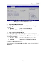
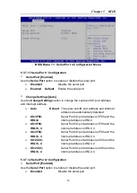
Page 80: ...k controller enabled Power Saving Function Disabled Use the Power Saving Function BIOS option to enable or reduce power consumption in the S5 state When enabled the system can only be powered up using the power button Disabled Default Power Saving Function support disabled Enabled Power Saving Function support enabled 5 3 7 1 Serial Port n Configuration Use the Serial Port n Configuration menu BIO...

Page 81: ...t address are automatically detected IO 3F8h IRQ 4 Serial Port I O port address is 3F8h and the interrupt address is IRQ4 IO 3F8h IRQ 3 4 Serial Port I O port address is 3F8h and the interrupt address is IRQ3 4 IO 2F8h IRQ 3 4 Serial Port I O port address is 2F8h and the interrupt address is IRQ3 4 IO 2C0h IRQ 3 4 Serial Port I O port address is 2C0h and the interrupt address is IRQ3 4 IO 2C8h IRQ...

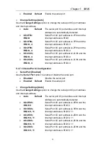
Page 82: ...rrupt address is IRQ3 4 5 3 7 1 3Serial Port 4 Configuration Serial Port Enabled Use the Serial Port option to enable or disable the serial port Disabled Disable the serial port Enabled Default Enable the serial port Change Settings Auto Use the Change Settings option to change the serial port IO port address and interrupt address Auto Default The serial port IO port address and interrupt address ...

Page 83: ...D8h and the interrupt address is IRQ10 IO 2C0h IRQ 10 11 Serial Port I O port address is 2C0h and the interrupt address is IRQ10 11 IO 2C8h IRQ 10 11 Serial Port I O port address is 2C8h and the interrupt address is IRQ10 11 IO 2D0h IRQ 10 11 Serial Port I O port address is 2D0h and the interrupt address is IRQ10 11 IO 2D8h IRQ 10 11 Serial Port I O port address is 2D8h and the interrupt address i...

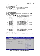
Page 84: ...ess is 378h and the interrupt address is IRQ7 IO 278h IRQ 7 Parallel Port I O port address is 278h and the interrupt address is IRQ7 IO 3BCh IRQ 7 Parallel Port I O port address is 3BCh and the interrupt address is IRQ7 Device Mode Printer Mode Use the Device Mode option to select the mode the parallel port operates in Configuration options are listed below Printer Mode Default SPP Mode EPP 1 9 an...

Page 85: ...shown The system parameters that are monitored are System Temperatures CPU Temperature System Temperature Fan Speeds CPU Fan Speed Voltages VCC3V Vcore Vcc 1 05V VDDR VSB3V VBAT 5VSB 5 3 8 1 FAN 1 Configuration Use the FAN 1 Configuration submenu BIOS Menu 14 to configure fan 1 temperature and speed settings ...

Page 86: ...settings Manual by Duty Cycle The fan spins at the speed set in Manual by Duty Cycle settings Target Temp Sensor CPU Temperature Use the Target Temp Sensor option to set the target CPU temperature CPU Temperature Default Sets the target temperature sensor to the CPU temperature SYS Temperature Sets the target temperature sensor to the System Temperature setting Temperature Bound n Use the or key t...

Page 87: ...ng keyboard input and text output through the serial port BIOS Menu 15 Serial Port Console Redirection Console Redirection Disabled Use Console Redirection option to enable or disable the console redirection function Disabled Default Disabled the console redirection function Enabled Enabled the console redirection function Terminal Type VT 100 Use the Terminal Type option to specify the remote ter...

Page 88: ...n speed at 38400 57600 Sets the serial port transmission speed at 57600 115200 Default Sets the serial port transmission speed at 115200 5 4 Chipset Use the Chipset menu BIOS Menu 16 to access the Northbridge Southbridge Integrated Graphics and ME Subsystem configuration menus WARNING Setting the wrong values for the Chipset BIOS selections in the Chipset BIOS menu may cause the system to malfunct...

Page 89: ...ics controller a PCI express PEG controller or an IGD Configuration options are listed below IGD PCI IGD PCI PEG PEG IGD Default PEG PCI IGD Memory 64M Use the IGD Memory option to specify the amount of system memory that can be used by the Internal graphics device Disable 32M 32 MB of memory used by internal graphics device 64M Default 64 MB of memory used by internal graphics device 96M 96 MB of...

Page 90: ...device 416M 416 MB of memory used by internal graphics device 448M 448 MB of memory used by internal graphics device 480M 480 MB of memory used by internal graphics device 512M 512 MB of memory used by internal graphics device PCI Express Port Enabled Use the PCI Express Port option to enable or disable the PCI Express port Disabled Disables the PCI Express port Enabled Default Enables the PCI Exp...

Page 91: ...e GbE controller Before disabling the GbE controller the AMT function must be disabled Disabled The onboard GbE controller is disabled Enabled Default The onboard GbE controller is enabled GbE PXE Boot Disabled Use the GbE PXE Boot option to enable or disable the boot option for GbE devices Disabled Default Disables the GbE PXE Boot option Enabled Enables the GbE PXE Boot option Restore on AC Powe...

Page 92: ...Enabled Default Enables Resume on PCI PME GbE option Resume on Ring Enabled Use the Resume on Ring option to enable or disable resuming from RI signal Disabled Disables Resume on Ring option Enabled Default Enables Resume on Ring option Resume on PS 2 Enabled Use the Resume on PS 2 option to enable or disable resuming from PS 2 activation Disabled Disables Resume on PS 2 option Enabled Default Ena...

Page 93: ...ion Enabled Enables PCIe LAN PXE Boot option 5 4 3 Integrated Graphics Use the Integrated Graphics menu BIOS Menu 19 to configure the video device connected to the system BIOS Menu 19 Integrated Graphics DVMT Mode Select DVMT Mode Use the DVMT Mode Select option to select the Intel Dynamic Video Memory Technology DVMT operating mode Fixed Mode A fixed portion of graphics memory is reserved as grap...

Page 94: ...evice used by the system when it boots For dual display support select Auto Configuration options are listed below AUTO Default CRT DVI 5 4 4 ME Subsystem Use the ME Subsystem menu BIOS Menu 20 to configure the Intel Management Engine ME configuration options BIOS Menu 20 ME Subsystem MEBx Mode Normal Use the MEBx Mode option to configure MEBx Mode options Normal Default Enables normal mode Hidden...

Page 95: ...the number lock setting must be modified during boot up On Default Allows the Number Lock on the keyboard to be enabled automatically when the computer system boots up This allows the immediate use of the 10 key numeric keypad located on the right side of the keyboard To confirm this the Number Lock LED light on the keyboard is lit Off Does not enable the keyboard Number Lock automatically To use ...

Page 96: ...eep Current Use the Option ROM Messages option to set the Option ROM display mode Force BIOS Sets display mode to force BIOS Keep Current Default Sets display mode to current 5 6 Security Use the Security menu BIOS Menu 22 to set system and user passwords BIOS Menu 22 Security Administrator Password Use the Administrator Password to set or change a administrator password User Password Use the User...

Page 97: ...e the Discard Changes and Reset option to exit the system without saving the changes made to the BIOS configuration setup program Restore Defaults Use the Restore Defaults option to load the optimal default values for each of the parameters on the Setup menus F3 key can be used for this operation Save as User Defaults Use the Save as User Defaults option to save the changes done so far as user def...
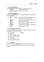
Page 98: ...SATA Port Disabled 77 Hot Plug Disabled 77 USB Devices 78 USB Support Enabled 78 Legacy USB Support Enabled 78 Floppy Disk Controller Enabled 79 Power Saving Function Disabled 79 Serial Port Enabled 80 Change Settings Auto 80 Serial Port Enabled 80 Change Settings Auto 81 Serial Port Enabled 81 Change Settings Auto 81 Serial Port Enabled 82 Change Settings Auto 82 Parallel Port Enabled 83 Change S...

Page 99: ... 91 Resume on PME GbE Enabled 91 Resume on Ring Enabled 91 Resume on PS 2 Enabled 91 Azalia HD Audio Enabled 91 PCIe LAN Controller Enabled 91 PCIe LAN PXE Boot Disabled 92 DVMT Mode Select DVMT Mode 92 DVMT Memory Maximum 93 IGD Boot Type AUTO 93 MEBx Mode Normal 93 Unconfigure AMT ME Disabled 94 Bootup NumLock State On 94 Quiet Boot Enabled 95 Option ROM Messages Keep Current 95 Administrator Pa...

Page 100: ... signal represents a binary 1 BIOS The Basic Input Output System BIOS is firmware that is first run when the computer is turned on and can be configured by the end user CODEC The Compressor Decompressor CODEC encodes and decodes digital audio data on the system CMOS Complimentary metal oxide conductor is an integrated circuit used in chips like static RAM and microprocessors COM COM refers to seri...

Page 101: ...plies with the IEEE 802 3 2005 standard GPIO General purpose input HDD Hard disk drive HDD is a type of magnetic non volatile computer storage device that stores digitally encoded data ICH The Input Output Control Hub ICH is an Intel Southbridge chipset IrDA Infrared Data Association IrDA specify infrared data transmission protocols used to enable electronic devices to wirelessly communicate with ...

Page 102: ...emented on hard disk drives UART Universal Asynchronous Receiver transmitter UART is responsible for asynchronous communications on the system and manages the system s serial communication COM ports UHCI The Universal Host Controller Interface UHCI specification is a register level interface description for USB 1 1 Host Controllers USB The Universal Serial Bus USB is an external bus standard for i...

Page 103: ...of external devices or TTL devices Data can be read or written to the selected address to enable the DIO functions NOTE For further information please refer to the datasheet for the Super I O chipset The BIOS interrupt call INT 15H controls the digital I O INT 15H AH 6FH Sub function AL 8 Set the digital port as INPUT AL Digital I O input value C 2 Assembly Language Sample 1 MOV AX 6F08H setting t...

Page 104: ...Appendix C Digital I O Interface 103 C 3 Assembly Language Sample 2 MOV AX 6F09H setting the digital port as output MOV BL 09H digital value is 09H INT 15H Digital Output is 1001b ...

Page 105: ...H AH 6FH Sub function AL 2 Sets the Watchdog Timer s period BL Time out value Its unit second is dependent on the item Watchdog Timer unit select in CMOS setup Table D 1 AH 6FH Sub function Call sub function 2 to set the time out period of Watchdog Timer first If the time out value is not zero the Watchdog Timer starts counting down When the timer value reaches zero the system resets To ensure tha...

Page 106: ...COUNTER W_LOOP MOV AX 6F02H setting the time out value MOV BL 30 time out value is 48 seconds INT 15H ADD THE APPLICATION PROGRAM HERE CMP EXIT_AP 1 is the application over JNE W_LOOP No restart the application MOV AX 6F02H disable Watchdog Timer MOV BL 0 INT 15H EXIT ...

Page 107: ...system as a contingent storage space The operating system will not be able to distinguish the physical disk drives contained in a RAID configuration E 1 1 Precautions One key benefit a RAID configuration brings is that a single hard drive can fail within a RAID array without damaging data With RAID1 array a failed drive can be replaced and the RAID configuration restored WARNING Irrecoverable data...

Page 108: ... in a RAID configuration If they are not the same size disk drive capacity is sacrificed and overall performance affected Step 2 Enable SATA drives in BIOS Start the computer and access the BIOS setup program Enable RAID support for all SATA devices Refer to the applicable BIOS configuration section in this user manual Step 3 Configure Option ROM Messages BIOS option to Force BIOS This is to allow...

Page 109: ...on another computer If installing on the RAID array a RAID driver floppy disk must be made The RAID driver floppy disk utility is on the CD in the 5 SATA Floppy Configuration Utility folder The floppy disk will be formatted and the drivers installed Step 2 Restart the system with a floppy drive attached Attach a normal floppy drive or USB floppy drive to the system Step 3 Press F6 when prompted Du...

Page 110: ...product to indicate the estimated Environmentally Friendly Use Period EFUP This is an estimate of the number of years that these substances would not leak out or undergo abrupt change This product may contain replaceable sub assemblies components which have a shorter EFUP such as batteries and lamps These components will be separately marked Please refer to the table on the next page Part Name Tox...

Page 111: ... materials for this part is above the limit requirement in SJ T11363 2006 此附件旨在确保本产品符合中国 RoHS 标准 以下表格标示此产品中某有毒物 质的含量符合中国 RoHS 标准规定的限量要求 本产品上会附有 环境友好使用期限 的标签 此期限是估算这些物质 不会 有泄漏或突变 的年限 本产品可能包含有较短的环境友好使用期限的可替换 组件 像是电池或灯管 这些元件将会单独标示出来 部件名称 有毒有害物质或元素 铅 Pb 汞 Hg 镉 Cd 六价铬 CR VI 多溴联苯 PBB 多溴二苯醚 PBDE 壳体 O O O O O O 显示 O O O O O O 印刷电路板 O O O O O O 金属螺帽 O O O O O O 电缆组装 O O O O O O 风扇组装 O O O O O O 电力供应组装 O O ...

Reviews: