background image


N58 Hardware User Guide 

Chapter  5  Application  Interfaces 


Copyright © Neoway Technology Co., Ltd. All rights reserved. 

37 


Soft 

shutdown 

is 

implemented 

by 

using 

AT 

commands. 

For 

details, 

see 

Neoway_

N58

_AT_Command_Manual

5.2.2 RESET_N 

The RESET_N pin is used to reset the N58 module. When the module is working properly, inputting a 

low-level pulse for more than 50 ms at the RESET_N pin can trigger the reset process of the module. 
RESET_N is connected to VBAT internally by using a 20 kΩ pull-up resistor. Leave this pin floating if it 
is not used. 

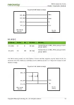
Figure 5-11 Module reset controlled by button 

ESD


N58 Module

RESET_N

S1

470

Ω

VBAT

20k

Ω

R2

R1


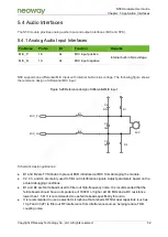
If the 1.8 V/2.8 V/3.0 V IO system is used, it is recommended that a triode be used for isolation. For 

details about the design, see the following figure. 

Figure 5-12 Reference reset circuit in which a triode is used for isolation 


N58 Module

RESET_N

VBAT

20k

Ω

R2

47k

Ω

Q1

R1

4.7k

Ω

_ON

USER

R3


Summary of Contents for N58

Page 1: ...Hardware User Guide Issue 2 5 Date 2021 10 29...

Page 2: ...GUIDE PROVIDES INSTRUCTIONS FOR CUSTOMERS TO DESIGN THEIR APPLICATIONS PLEASE FOLLOW THE RULES AND PARAMETERS IN THIS GUIDE TO DESIGN AND COMMISSION NEOWAY WILL NOT TAKE ANY RESPONSIBILITY OF BODILY H...

Page 3: ...17 4 Module Pins 18 4 1 Pin Layout 18 4 2 Pin Description 19 5 Application Interfaces 28 5 1 Power Interface 28 5 1 1 VBAT 28 5 1 2 VDD_1P8 33 5 2 Control Interface 33 5 2 1 PWRKEY_N 33 5 2 2 RESET_N...

Page 4: ...8 6 Electrical Characteristics and Reliability 71 6 1 Electrical Characteristics 71 6 2 Temperature Characteristics 72 6 3 ESD Protection Characteristics 72 7 RF Characteristics 73 7 1 Operating Bands...

Page 5: ...lled by button 37 Figure 5 12 Reference reset circuit in which a triode is used for isolation 37 Figure 5 13 Reset process of the N58 module 38 Figure 5 14 Process of entering the sleep mode 39 Figure...

Page 6: ...5 37 1PPS output waveform 62 Figure 5 38 Reference design of GNSS active antenna power supply and detection circuit 63 Figure 5 39 L type matching network 64 Figure 5 40 T type matching network 64 Fig...

Page 7: ...on of LCD function pins 55 Table 5 2 Description of camera function pins 56 Table 6 1 Electrical characteristics of the N58 module 71 Table 6 2 Current consumption of the N58 module typical 71 Table 6...

Page 8: ...11 Initial release Zhang Gang 2 0 2020 05 Changed the definitions of pins 13 78 80 and 83 Updated the GNSS characteristics and added the support for BDS Updated the frequency bands of EA and LA varian...

Page 9: ...mmended circuit of a USIM card to explain the handling method of the USIM_DET pin when a user uses hot plug or does not use hot plug Deleted the description of adaptive because an SD card does not sup...

Page 10: ...meters Added the reference design of the passive GNSS antenna circuit Updated the label diagram Updated the table of abbreviations Optimized the document to improve its quality Conventions Symbol Desc...

Page 11: ...er Guide About This Document Copyright Neoway Technology Co Ltd All rights reserved xi Related Documents Neoway_N58_Datasheet Neoway_N58_Product_Specifications Neoway_N58_AT_Command_Mannual Neoway_N58...

Page 12: ...r a fire Disable the wireless communication function in places where wireless communication is prohibited Do not use this product that can interfere with other electronic devices in environments such...

Page 13: ...characteristics ARM Cortex A5 processor 500 MHz main frequency 32 KB L1 cache Supported network modes GSM GPRS LTE Cat 1 Support for USB2 0 USIM ADC UART SDIO SPI I2C and GNSS optional 2 1 Product Ov...

Page 14: ...its Baseband chip unit 26 MHz crystal Power manager RF functional unit Digital interfaces including USIM I2C SPI KEYPAD UART USB and SDIO Analog interfaces ADC MIC and SPK Figure 2 1 Block diagram VBA...

Page 15: ...Max 85 6 kbps UL FDD LTE Cat 1 Max 10 Mbps DL Max 5 Mbps UL TDD LTE Cat 1 Max 8 Mbps DL Max 2 Mbps UL Power class GSM850 33 dBm Power Class 4 EGSM900 33 dBm Power Class 4 DCS1800 30 dBm Power Class 1...

Page 16: ...ode2 indicates that the module enters the low power consumption state In this state the peripheral interface of the module is disabled but the radio frequency function is normal The module will exit t...

Page 17: ...and IC card requirements 3GPP TS 51 011 V4 15 0 Specification of the Subscriber Identity Module Mobile Equipment SIM ME interface 3GPP TS 31 102 V13 0 0 Characteristics of the Universal Subscriber Ide...

Page 18: ...GPS_LNA_EN GND SDC_DET USB_BOOT VDD_1P8 USB_VBUS VBAT RESERVED GND GND GND GND NET_LIGHT SPI_CLK SPI_MISO SPI_CS_N ADC ANT_GNSS GND ANT_BT USB_DP USB_DM USIM1_DET USIM1_RESET USIM1_CLK USIM1_DATA USI...

Page 19: ...acteristics P1 Dual voltage USIM interface voltage type 1 8 V or 3 V 1 8 V DC characteristics VIH 1 26 V to 1 98 V VIL 0 V to 0 54 V VOH 1 44 V to 1 98 V VOL 0 V to 0 36 V 3 V DC characteristics VIH 2...

Page 20: ...on power off This pin is connected to VBAT by using a 20 k pull up resistor in the main chip of the module SLEEP 79 DI Sleep mode control P3 See section 5 2 3 SLEEP UART1 interface UART1_TXD 69 DO Dat...

Page 21: ...tput P1 USIM1_DATA 36 B USIM1 data input output P1 Connect this pin to USIM1_VCC by using a 4 7 k pull up resistor USIM1_CLK 37 DO USIM1 clock output P1 USIM1_RESET 38 DO USIM1 reset P1 USIM1_DET 39 D...

Page 22: ...gnal 12 bit Detectable voltage range 0 1 V to VBAT Leave this pin floating if it is not used I2C interface I2C_SDA 81 B I2C data P3 Connect this pin to VDD_1P8 by using a 1 8 k pull up resistor I2C_SC...

Page 23: ...cklight LED The anode power supply range is 3 45 V to 4 3 V and the maximum input current is 50 mA LED_K2 141 PI Backlight LED The anode power supply range is 3 45 V to 4 3 V and the maximum input cur...

Page 24: ...ting if it is not used SDC_DATA_2 3 B SDIO data bit 2 1 8 V 3 0 V Leave this pin floating if it is not used SDC_DATA_3 4 B SDIO data bit 3 1 8 V 3 0 V Leave this pin floating if it is not used SDC_CMD...

Page 25: ...put from the master device P3 Leave this pin floating if it is not used SPI_CS_N 87 DO Chip select signal of the slave device P3 Leave this pin floating if it is not used GPIO interface GPIO_0 50 B GP...

Page 26: ...pin floating if it is not used VRTC 113 PI RTC power supply 2 8 V to 3 2 V typical value 3 0 V It can be connected to a coin battery or farad capacitor and provides RTC power supply Leave this pin fl...

Page 27: ...d pins Used for future function expansion or functions that are not open to users There may be more than one pin named RESERVED but it does not mean that the RESERVED pins have the same function or de...

Page 28: ...o I O Function Remarks VBAT 27 28 29 PI Power input of the module 3 4 V to 4 2 V typical value 3 8 V VDD_1P8 45 PO 1 8 V power output Vnorm 1 8 V Imax 50 mA GND 1 14 17 20 26 30 31 44 49 74 75 77 91 9...

Page 29: ...these two characteristics will cause the operating voltage of the module to be unstable and even damage the module The power supply design of the N58 module is determined by the power input voltage Th...

Page 30: ...e power supply The following circuit design is recommended if the power supply needs to be controlled Figure 5 3 Recommended design 2 S G D R4 100 k C4 10 F Q2 Q1 C3 470 F C5 0 1 F C6 100pF C7 33 pF R...

Page 31: ...so that the power surge voltage is clamped before it enters back end circuits protecting the back end components and the module Place C4 close to the module A large capacity aluminum electrolytic capa...

Page 32: ...s voltage spikes and protect back end components The circuit design is important and the component layout and traces are also important Several key points in power supply design are summarized below T...

Page 33: ...urrent is 50 mA 5 2 Control Interface Pin Name Pin No I O Function Remarks RESET_N 32 DI Module reset input Triggered by low level PWRKEY_N 33 DI Module power on power off control Triggered by low lev...

Page 34: ...All rights reserved 34 Figure 5 6 Reference design of module startup controlled by button N58 Module VBAT 1k 20k R1 R2 Main Chip ESD PWRKEY_N S1 470 R3 Figure 5 7 Reference design of module startup c...

Page 35: ...the external external resistor connected to the ground in serial connection mode cannot be excessively large the recommended resistor resistance in serial connection mode is 470 Otherwise the module...

Page 36: ...ss Two methods are available to shut down the module hard shutdown and soft shutdown Hard shutdown is implemented by using the PWRKEY_N pin When the module is working properly inputting a low level pu...

Page 37: ...at the RESET_N pin can trigger the reset process of the module RESET_N is connected to VBAT internally by using a 20 k pull up resistor Leave this pin floating if it is not used Figure 5 11 Module re...

Page 38: ...ive Active T 50ms UART Active 5 2 3 SLEEP The SLEEP pin is the control pin of the sleep mode and it needs to be used together with AT commands Related AT commands can be sent over the UART2 interface...

Page 39: ...sleep mode Sleep mode MCU detects information from UART MCU pulls SLEEP pin to high End Enable UART and process services MCU pulls SLEEP pin to low Wait till services are processed Complete service pr...

Page 40: ...nt the wake up function the reference design of the N58 module sleep and wake up control circuit is recommended as shown in Figure 5 17 Entering the sleep mode exiting from the sleep mode AT ENPWRSAVE...

Page 41: ...e of the module are based on the module whereas peripheral pins are named based on peripheral components For example UART_TXD indicates the pin used by the module to send data and MCU_RXD indicates th...

Page 42: ...R1 GND USB_DM USB_VBUS N58 Module USB Host VCC 4 5 V 5 2 V D2 D3 GND C2 C1 D1 USB_DP R2 USB_DM USB_DP Schematic design guidelines Connect C1 1 F and C2 33 pF filter capacitors in parallel to the USB_...

Page 43: ...of the module UART1_RXD 70 DI Data receiving UART1_CTS 71 DI User allowing the module to send data UART1_RTS 72 DO Module requesting the user to send data UART2_TXD 46 DO Data sending Software standar...

Page 44: ...required Three types of level shifting circuits are recommended to meet different logic level and rate requirements If the UART interface baud rate is higher than 115200 bps it is recommended to use...

Page 45: ...and is recommended to use level shifting circuit 3 see Figure 5 22 for UART interface CTS and RTS Figure 5 21 Recommended level shifting circuit 2 C1 C2 10pF UART_RXD 10 k 100 k 10 k VDD_1P8 10k 10pF...

Page 46: ...ce the smaller the value of R2 R4 R1 R3 4 7 k to 10 k The higher the working rate of the UART interface the smaller the value of R1 R3 Q1 Q2 MMBT3904 or MMBT2222 High rate transistors are better 5 3 3...

Page 47: ...C4 C5 C6 D1 20 R1 20 R2 20 R3 20 R4 D2 D3 D4 D5 R6 Schematic design guidelines USIM_VCC is the pin for supplying power only to USIM cards and its maximum load capacity is 50 mA USIM_VCC cannot be used...

Page 48: ...rd does not use the hot plug function the USIM_DET pin of the N58 module must be pulled up to 1 8 V by using a 47 k resistor in series and the software must disable the USIM hot plug detection functio...

Page 49: ..._DET 96 DI SD detection VDD_SDCPULL 103 PO Pull up power supply for the SD card SDIO bus It is forbidden to supply power to other loads Leave this pin floating if it is not used The SDIO interface sup...

Page 50: ...riggering interruption You can choose to configure the effective level of insertion detection as high or low level by using software based on the structure of the card connector PCB design guidelines...

Page 51: ...DA 81 B I2C data Connect this pin to VDD_1P8 by using a 1 8 k pull up resistor I2C_SCL 82 DO I2C clock Connect this pin to VDD_1P8 by using a 1 8 k pull up resistor The N58 module provides one I2C int...

Page 52: ...fferential MIC input B1 B2 DNI DNI DNI MIC_P MIC_N C2 C3 C4 D1 D2 MIC Schematic design guidelines D1 and D2 are TVS diodes to prevent ESD introduced at MIC from damaging the module C2 C3 and C4 are ma...

Page 53: ...itive Support for only differential output built in class AB or class D power amplifier Maximum output power Class AB 600 mW 4 2 V 8 load Class D 800 mW 4 2 V 8 load SPK_N 16 AO Speaker output negativ...

Page 54: ...traces to reduce radiation interference Power traces must not be parallel to audio traces and should be as far away from audio traces as possible Differential audio traces comply with the rules of di...

Page 55: ...in Name Pin No I O Function Remarks LCD_RST_N 63 DO Reset control LCD_TE 64 DO Data frame read ready flag LCD_SPI_CS 65 DO SPI chip select signal LCD_SPI_CLK 66 DO SPI clock signal LCD_SPI_SDC 67 B Da...

Page 56: ...al input CAM_SPI_CLK 57 DO SPI clock signal CAM_I2C_SDA 58 B I2C data CAM_I2C_SCL 59 DO I2C clock CAM_PWDN 60 DO Power off control CAM_MCLK 61 DO Master clock signal AVDD_CAM 62 PO Camera analog power...

Page 57: ...t is recommended to drive an LED indicator by controlling a triode The following figure shows the reference design of driving an LED indicator by controlling a triode Figure 5 31 Reference design of d...

Page 58: ...0ms 5 6 4 USB_BOOT Pin Name Pin No I O Function Remarks USB_BOOT 48 DI Forcible download control USB_BOOT is the pin for forcible download control Connect USB_BOOT to VDD_1P8 by using a pull up resist...

Page 59: ...rcuits The voltage range is 3 0 V to 3 3 V Leave this pin floating if it is not used To use the hot start function of GNSS and save the positioning data connect it to a backup power supply or keep con...

Page 60: ...O with the interruption function Leave this pin floating if it is not used GPIO_2 80 B GPIO with the interruption function Leave this pin floating if it is not used GPIO_3 78 B GPIO with the interrupt...

Page 61: ...ut Leave this pin floating if it is not used KEYOUT0 133 DO Key output Leave this pin floating if it is not used KEYIN1 134 DI Key input Leave this pin floating if it is not used KEYIN2 135 DI Key inp...

Page 62: ...PS pin can be used as the ADC pin The detectable voltage ranges from 0 1 V to VBAT and 12 bit precision resolution is supported 5 6 10 VCC_GNSS_BIAS Pin Name Pin No I O Function Remarks VCC_GNSS_BIAS...

Page 63: ...Module SMA ANT_GNSS GNSS_ANT_BIAS NC NC 33pF 33pF 47 100nH 5 7 RF Interfaces Pin Name Pin No I O Function Remarks ANT_MAIN 76 2G 4G main antenna pin 50 impedance characteristics ANT_GNSS 92 GNSS ante...

Page 64: ...Z2 D1 Z3 Figure 5 41 type matching network ANT_MAIN N58 Module Z1 Z2 D1 Z3 Schematic design guidelines Components in the above figures must be capacitors inductors and 0 resistors Place these RLC com...

Page 65: ...der pad might result in great parasitic capacitance which will affect the antenna performance Remove the copper on the first and fourth layers or all layers of a multiple layer PCB under the RF solder...

Page 66: ...to section 5 7 1 ANT_MAIN Antenna Interface If using a passive GNSS antenna place an LNA near the antenna feed point because the module does not embed an LNA internally The GNSS_LNA_EN pin is used to...

Page 67: ...na by using an inductance of 47 nH to 100 nH The common active antenna requires 3 3 V to 5 V power supply The active antenna itself has small power consumption but requires a low noise factor LDO to s...

Page 68: ...ooth antenna interface refer to section 5 7 1 ANT_MAIN Antenna Interface The ANT_BT interface is shared by Wi Fi signal reception This interface can support both Wi Fi and BT BLE 5 7 4 Antenna Assembl...

Page 69: ...e RF cable to the module by soldering This method is not recommended because it has stability consistency and RF performance degradation problems The following figure shows the module RF connection me...

Page 70: ...ace it is recommended to adopt the layout shown in Figure 5 48 a 1 chip antenna 2 mark of the antenna feed end 3 matching circuit pad 4 50 impedance cable 5 in Figure 5 48 is the area between the ante...

Page 71: ...or DC DC to supply power to the module ensure that the output instantaneous current is at least 2 5 A The 2 5 A current occurs when the module is working at the maximum power level of the GSM mode Th...

Page 72: ...rate and fail to comply with 3GPP specifications However it will not have a large impact on the normal use of the module After the temperature is restored the RF performance indicators of the module c...

Page 73: ...Hz EGSM900 880 915 MHz 925 960 MHz DCS1800 1710 1785 MHz 1805 1880 MHz PCS1900 1850 1910 MHz 1930 1990 MHz FDD LTE B1 1920 1980 MHz 2110 2170 MHz FDD LTE B2 1850 1910 MHz 1930 1990 MHz FDD LTE B3 1710...

Page 74: ...3 dBm 2 dB 40 dBm FDD LTE B3 23 dBm 2 dB 40 dBm FDD LTE B4 23 dBm 2 dB 40 dBm FDD LTE B5 23 dBm 2 dB 40 dBm FDD LTE B7 23 dBm 2 dB 40 dBm FDD LTE B8 23 dBm 2 dB 40 dBm FDD LTE B20 23 dBm 2 dB 40 dBm F...

Page 75: ...andwidth QPSK modulation and RBs whose quantity is in accordance with the conditions stipulated in the protocol The RX sensitivity of certain frequency bands on the live network without shielding may...

Page 76: ...ive antenna The tracking sensitivity and the acquisition sensitivity were obtained in a signaling test on SPIRENT6300 and they are the maximum values in multiple tests on samples During the tests no e...

Page 77: ...cal Characteristics Copyright Neoway Technology Co Ltd All rights reserved 77 8 Mechanical Characteristics This chapter describes the mechanical characteristics of the N58 module 8 1 Dimensions Figure...

Page 78: ...bel examples The pictures above are only for reference 8 3 Packaging The N58 module uses a surface mount method for furnace welding A moisture proof packaging method is used to prevent the product fro...

Page 79: ...8 3 1 Reel and Tape N58 modules in mass production are delivered in the following packaging Tape details DIM ITEM TOLE T 44 0 W 2 0 P2 36 0 P 0 3 0 3 0 1 0 1 0 05 0 30 3 55 K0 1 75 F E 20 2 0 1 0 10 0...

Page 80: ...if it is exposed to the air for a long time the module will be moist and the module may be damaged during reflow soldering or welding in a lab It is recommended that the module exposed to the air for...

Page 81: ...ay Technology Co Ltd All rights reserved 81 9 Assembly This chapter describes the N58 module package the recommended application package and technical points related to SMT 9 1 Module PCB Package Figu...

Page 82: ...es the LGA 100 pins LCC 92 pins package The recommended PCB package is as follows To ensure the normal operation of the module there can be only GND vias and pour copper under the shadow areas of the...

Page 83: ...pastes without lead and less time is consumed correspondingly It is easy to cause the LCC LGA in the module to be in the semi melted state after the second reflow soldering resulting in poor soldering...

Page 84: ...ortant notes in N58 storage and mounting refer to Neoway_Reflow_Soldering_Guidelines_For_Surface Mounted_Modules When manually desoldering the module use heat guns with great opening adjust the temper...

Page 85: ...ompulsory Certification CEP Circular Error Probable CNR Carrier to Noise Rate CS Chip Select CTS Clear to Send DC Direct Current DCS Digital Cellular System DI Digital Input DIO Digital Input Output D...

Page 86: ...al Packet Radio Service GPS Global Positioning System GSM Global System for Mobile Communications I2C Inter Integrated Circuit IO Input Output ISP Image Signal Processor LCC Leadless Chip Carriers LCD...

Page 87: ...TDD Time Division Duplex UART Universal Asynchronous Receiver Transmitter UL Uplink USB Universal Serial Bus USIM Universal Subscriber Identity Module VBAT Battery Voltage VSWR Voltage Standing Wave R...

Reviews: