N58 Hardware User Guide
Chapter 5 Application Interfaces
Copyright © Neoway Technology Co., Ltd. All rights reserved.
67
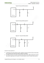
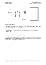
Figure 5-44 Reference design of an active GNSS antenna
LNA
Active
Antenna
N58 Module
LDO
2.2
μ
F
33pF
47~100nH
33pF
Z1
Z2
Z3
VIN
EN
PCB design guidelines:
For guidelines of PCB design between the GNSS interface and antenna, refer to PCB design
guidelines in section 5.7.1 "ANT_MAIN Antenna Interface."
50 Ω impedance is required for the feeder and PCB traces, and the traces should be as short as
possible. The power of the active antenna is fed from the signal cable of the antenna by using an
inductance of 47 nH to 100 nH.
The common active antenna requires 3.3 V to 5 V power supply. The active antenna itself has
small power consumption, but requires a low noise factor LDO to supply power to the antenna by
using an inductance of 47 nH to 100 nH, as shown in the preceding figure.
Keep the GNSS RF part far away from the main/BT antenna part. Otherwise, these two parts will
interfere with each other, affecting the RF performance. If the layout is not well designed, it may
interfere with GNSS and affect performance.
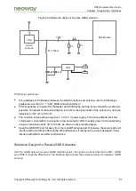
Reference Design of a Passive GNSS Antenna
After the GNSS antenna receives GNSS satellite signals, the signals are transmitted to the ANT_GNSS
pin of N58 through the PCB traces. The following figure shows the reference design of a passive GNSS
antenna.

