background image


N723-EA Hardware User Guide   

Chapter 5 Application Interfaces 


Copyright © Neoway Technology Co., Ltd. All rights reserved. 

36 


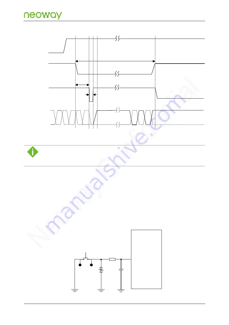
Figure 5-12 

Hardware shutdown process 

PWRKEY_N

VBAT

UART

VDD_1P8

3.75s

T

18s

310ms

Active

Off

Inactive

Indefinite


When the module executes the shutdown process, VDD_1P8 stops the voltage output after the UART port 
completes the shutdown process. The low pulse width needed for RESET_N hard shutdown may slightly vary 
with the module software. 

5.2.3 

USB_BOOT 

USB_BOOT is the pin to forcibly enter the download mode. Connect USB_BOOT to GND through a 
pull-down resistor after the module is started, and the module will enter forcible download mode. This 
is  the  last  method  to  handle  issues  that  result  in  startup  or  running  failures.  It  is  recommended  to 
reserve this pin (as a button or a test point) to facilitate software upgrades and debugging.   

The following figure shows a reference design of USB force download: 

Figure 5-13 

Reference design of USB force download 

USB_BOOT

N723-EA

Module

TVS

D1

470

Ω 

R1

Test point

C1

0.1

μF 


Summary of Contents for N723-EA

Page 1: ...Hardware User Guide Issue 1 0 Date 2022 06 02 ...

Page 2: ...HIS GUIDE PROVIDES INSTRUCTIONS FOR CUSTOMERS TO DESIGN THEIR APPLICATIONS PLEASE FOLLOW THE RULES AND PARAMETERS IN THIS GUIDE TO DESIGN AND COMMISSION NEOWAY WILL NOT TAKE ANY RESPONSIBILITY OF BODILY HURT OR ASSET LOSS CAUSED BY IMPROPER OPERATIONS THE INFORMATION IN THIS DOCUMENT IS SUBJECT TO CHANGE WITHOUT NOTICE DUE TO PRODUCT VERSION UPDATE OR OTHER REASONS EVERY EFFORT HAS BEEN MADE IN PR...

Page 3: ...P8 30 5 2 Control Interfaces 30 5 2 1 PWRKEY_N 31 5 2 2 PWRKEY 32 5 2 3 USB_BOOT 36 5 2 4 SLEEP 37 5 3 Peripheral Interfaces 39 5 3 1 USB 39 5 3 2 UART 41 5 3 3 USIM 45 5 3 4 SD eMMC 47 5 3 5 I2S 48 5 3 6 SPI 49 5 3 7 I2C 50 5 4 Network and Connection 51 5 4 1 Ethernet 51 5 4 2 SDIO WLAN 53 5 5 GPIO interfaces 55 5 6 RF Interface 55 5 6 1 ANT_MAIN ANT_DIV Antenna Interfaces 55 5 6 2 Antenna Assemb...

Page 4: ...ion 63 7 RF Characteristics 64 7 1 Operating Band 64 7 2 TX Power and RX Sensitivity 65 8 Mechanical Characteristics 67 8 1 Dimensions 67 8 2 Label 68 8 3 Packing 68 8 3 1 Tray 68 8 3 2 Moisture 69 9 Mounting 70 9 1 PCB Package 70 9 2 Application Foot Print 71 9 3 Stencil 71 9 4 Solder Paste 72 9 5 SMT Oven Temperature Profile 72 Abbreviation 74 ...

Page 5: ...trolling PWRKEY_N 33 Figure 5 10 Startup process by controlling PWRKEY 34 Figure 5 11 Reset process of the module 35 Figure 5 12 Hardware shutdown process 36 Figure 5 13 Reference design of USB force download 36 Figure 5 14 Process of entering the sleep mode 37 Figure 5 15 Process of exiting from sleep mode 38 Figure 5 16 Incoming call service process 38 Figure 5 17 Outgoing call service process 3...

Page 6: ...rk 56 Figure 5 34 π type network 56 Figure 5 35 Recommended RF PCB design 57 Figure 5 36 Murata RF connector encapsulation specifications 58 Figure 5 37 RF cable connections 58 Figure 5 38 Antenna layout 59 Figure 5 39 Layout around the antenna 59 Figure 5 40 Pulse wave for an incoming call 60 Figure 5 41 RING indicator for SMS 61 Figure 5 42 Driving LED with a triode 61 Figure 8 1 N723 EA dimensi...

Page 7: ... I2C interface parameters 50 Table 5 2 Pin definition description 60 Table 6 1 N723 EAElectrical Characteristics 62 Table 6 2 N723 EA current consumption Typical 62 Table 6 3 N723 EA temperature features 63 Table 6 4 N723 EA ESD protection features 63 Table 7 1 N723 EA operating bands 64 Table 7 2 N723 EA RF transmit power 65 Table 7 3 GSM RX sensitivity of N723 EA 65 Table 7 4 N723 EA WCDMA RX se...

Page 8: ...s SEs development engineers and test engineers Change History Issue Date Change Changed By 1 0 2022 04 Initial draft Zou Shiqiang Conventions Symbol Indication Indicates danger or warning This information must be followed Otherwise a catastrophic module or user device failure or bodily injury may occur Indicates caution This symbol alerts the user to important points about using the module If thes...

Page 9: ...de About This Document Copyright Neoway Technology Co Ltd All rights reserved ix Related Documents Neoway_N723 EA_Datasheet Neoway_N723 EA_Product_Specifications Neoway_N723 EA_AT_Commands_Mannual Neoway_N723 EA_EVK_User_Guide ...

Page 10: ...n environments such as hospital or airplane where it might interfere with other electronic equipment If the product is used in medical institutions or on airplanes electromagnetic waves emitted by this product may interfere with surrounding equipment Please follow the requirements below in application design Do not disassemble the module without permission from Neoway Otherwise we are entitled to ...

Page 11: ...cle handheld POS industrial routers and so on N723 EA has the following characteristics ARM Cortex R5 processors 832 MHz main frequency at most 32 kB L1 command cache 32 kB L1 data cache Supported network modes LTE Cat 4 WCDMA GSM Supports interfaces I2S PCM RMII USIM USB2 0 UART SDIO SD eMMC I2C and SPI Table 2 1 lists the variant and frequency bands that N723 EA supports Table 2 1 Variant and fr...

Page 12: ...ower Bus SD eMMC 2 3 Basic Features Parameter Description Physical features Dimensions 30 00 0 10 mm 28 00 0 10 mm 2 95 0 20 mm Package LGA Weight about 5 10 g Temperature ranges Operating 30 C to 75 C Extended1 40 C 85 C Storage 40 C to 90 C Operating voltage VBAT 3 4 V 4 2 V typical value 3 8 V Operating current Sleep2 4 0 mA Idle3 35 mA Operating4 LTE mode 630mA Application processor ARM Cortex...

Page 13: ...6 dBm Power Class E2 WCDMA 23 dBm Power Class 3 LTE 23 dBm Power Class 3 Application interfaces 2G 3G 4G antenna 4G diversity RX antenna All of each has a characteristic impedance of 50 Ω Three UART interfaces one of which is a Debug UART interface One USIM interface 1 8V 3 0V adaptive One USB 2 0 interface One SDIO interface used for WLAN One SD eMMC interface used for SD card or eMMC One PCM I2S...

Page 14: ... but the radio frequency RF is functioning properly The module will exit the sleep mode when there is an incoming call or SMS message and will re enter the sleep mode at the end of the incoming call or conversation Standby mode3 the module is in normal working state but there is no on going data service Operating mode4 refers to the working current of the module when there is data communication On...

Page 15: ...o Resource Management RRM conformance testing 3GPP TS 21 111 V9 0 0 USIM and IC card requirements 3GPP TS 31 102 V9 19 0 Characteristics of the Universal Subscriber Identity Module USIM application 3GPP TS 31 111 V9 12 2 Universal Subscriber Identity Module USIM Application Toolkit USAT 3GPP TS 27 007 V9 9 0 AT command set for User Equipment UE 3GPP TS 27 005 V9 0 1 Use of Data Terminal Equipment ...

Page 16: ...SB_DM USIM_DET USIM_RESET USIM_CLK USIM_DATA USIM_VCC PWRKEY PWRKEY_N RESERVED GND GND GND GND SDC_PWR_EN SDC_DATA2 SDC_DATA3 SDC_CMD SDC_CLK SDC_DATA0 SDC_DATA1 I2S_SCLK I2S_TX I2S_RX I2S_WS RING GND RMII_TX_D1 RMII_TX_D0 GND RMII_RX_D1 RMII_RX_D0 GND RMII_CLK MDIO_CLK MDIO_DATA RMII_RX_DV RMII_TX_EN 1 I2S I2C SPI Control part RMII WLAN GND POWER 26 GND RESERVED GPIO_13 GPIO_04 UART2_RXD UART2_TX...

Page 17: ... Pin description AI Analog input AO Analog output AIO Analog input output B Digital Input Output DI Digital Input DO Digital Output PI Power input PO Power output Table 4 2 Level feature Interface type Power domai n Power domain description Power domain features Logic level USIM P1 USIM interface 1 8 V 3 0 V self adaptive 1 8 V level feature IH DD_P1 DD_P1 0 7 V V 0 2V V IL DD_P1 0 3V 0 3 V V OH M...

Page 18: ...L 0 3V 0 8 V V OH Min 2 4V V OL Max 0 4V V If you need to use the PCM I2S or RMII function contact Neoway FAEs The power domains of PWRKEY_N is VBAT and direct connection of GPIOs in different power domains is prohibited as that will result in voltage backflow RMII only supports 1 8 V level by default If supporting 3 3 V level is required ensure that the hardware supports it SD eMMC supports 1 8 V...

Page 19: ... 77 91 93 95 97 98 99 100 Ensure that all GND pins are grounded Control Interfaces PWRKEY_N 33 DI Used to power on off or reset the module Power on off reset of the module is triggered by the low pulse and is controlled based on the low pulse width The interface voltage is default to VBAT PWRKEY 34 DI Startup control Power on of the module is triggered by the high level Leave this pin floating if ...

Page 20: ..._DATA1 8 B SD eMMC data 1 P2 Leave this pin floating if it is not used SDC_DET 96 DI SD eMMC detect input P3 Leave this pin floating if it is not used USIM2 Interfaces I2S_SCLK 9 DO I2S data clock P3 Leave this pin floating if it is not used I2S_TX 10 DO I2S data sending P3 Leave this pin floating if it is not used I2S_RX 11 DI I2S data receiving P3 Leave this pin floating if it is not used I2S_WS...

Page 21: ... Leave this pin floating if it is not used MDIO_DATA 23 B MDIO data P4 Connecting a 4 7 kΩ external pull up resistor is required Leave this pin floating if it is not used USIM Interface USIM_VCC 35 PO USIM power output P1 Iomax 50 mA USIM_DATA 36 B USIM data input and output P1 Connecting a 4 7 kΩ pull up resistor to USIM_VCC is required USIM_CLK 37 DO USIM clock output P1 Leave this pin floating ...

Page 22: ...UG_UART1_TXD 65 DO Data transmitting P3 Only used for debug Leave this pin floating if it is not used DEBUG_UART1_RXD 66 DI Data receiving P3 UART2_TXD 69 DO Data transmitting P3 Used for data transmission Leave this pin floating if it is not used UART2_RXD 70 DI Data receiving P3 SDIO Interface WLAN_SDIO_CMD 54 B SDIO command P3 Leave this pin floating if it is not used WLAN_SDIO_CLK 55 DO SDIO c...

Page 23: ...n to VDD_1P8 through a pull up resistor externally is required for details see 5 3 7 I2C_SCL 82 DO I2C clock P3 SPI interface SPI_CLK 84 DO Clock signal P3 Supporting only master mode Leave this pin floating if it is not used SPI_MISO 85 DI Output of the slave device and input of the master device P3 SPI_MOSI 86 DO Input of the slave device and output of the master device P3 SPI_CS_N 87 DO Chip se...

Page 24: ... Ω impedance characteristics ANT_DIV 94 Diversity antenna 50 Ω impedance characteristics Other Interfaces RING 13 DO Incoming call indicator control P3 Leave this pin floating if it is not used NET_LIGHT 83 DO Network indicator control P3 Leave this pin floating if it is not used RESERVED RESERVED 32 50 53 73 80 88 89 92 Used for function extension or the function not open to users These RESERVE p...

Page 25: ... performance Signal Pin I O Function description Remarks VBAT 27 28 29 PI Power input of the module Vmin 3 4 V Vnorm 3 8 V Vmax 4 2V VDD_1P8 45 PO 1 8 V power output Vnorm 1 8V Imax 50 mA GND 1 14 17 20 26 30 31 44 49 74 75 77 91 93 95 97 98 99 100 Ensure that all GND pins are grounded 5 1 1 VBAT The power supply design covers two parts schematic design and PCB layout Power Supply Design In GSM GP...

Page 26: ...f forward voltage drop will lead to unstable operating voltage of the module or even damage the module The power supply design of the N723 EA module is determined by the power input voltage The designs are classified by power input voltage as follows Supports the 3 4V 4 2 V power input typical value 3 8 V using the battery for power supply Supports the 4 2V 5 5 V power input typical value 5 0 V us...

Page 27: ... module to filter out high frequency jamming from the power supply The following circuit design is recommended to control the power supply Figure 5 3 Recommended design 2 C1 C2 100kΩ R3 C8 C9 10kΩ R4 Q2 C B E 4 7kΩ R1 47kΩ R2 0 1μF 22μF C3 C4 C5 C6 C7 100μF 10μF 0 1μF 100pF 33pF VIN 3 8V PWR_EN VBAT 1μF 0 1μF S D G Q1 Select an enhanced p MOSFET at Q1 of which the safe operating voltage is at leas...

Page 28: ...of power supply is close to the permissible voltage across VBAT It is recommended to select an LDO that its maximum output current be greater than 2 5 A at U1 The TVS diode selected at D1 has a reverse operating voltage VRWM of 4 5 V and its peak power Ppp is 2800 W tp 8 20 uS It has the surge protection mechanism Place the TVS close to the power input interface to clamp the surge voltage before i...

Page 29: ... refer to the specifications of the chip Note that the switching frequency of the DC DC power supply is related to the device performance and may cause EMI interference For vehicle batteries lead acid batteries power surge protection should be added to the input front end and the device withstand voltage should be greater than 42 V Place C7 close to the module A large tantalum electrolytic capacit...

Page 30: ... frequency of the SW pin of the DC DC power supply is high and the loop should be minimized Sensitive component should be kept far away from the SW pin of the DC DC component to prevent noise coupling Feedback component should be placed as close as possible to the FB pin and COMP pin The GND pin and bottom pad of the chip must be grounded to ensure good heat dissipation and noise isolation 5 1 2 V...

Page 31: ...5 6 shows the reference design of starting the module by using a button Figure 5 7 shows the reference design of starting the module through an MCU Figure 5 8 shows the reference design of automatic start once powered up 5 2 1 PWRKEY_N PWRKEY_N supports the following functions When the module is in shut down state inputting negative pulses for more than 0 5s to PWRKEY_N can trigger the power on st...

Page 32: ...ontrolled by an MCU PWRKEY_N N723 EA Module 50kΩ VBAT R1 4 7kΩ R3 47kΩ R4 Q1 MCU_GPIO 1kΩ R2 0 1μF C1 TVS D1 Do NOT connect an external resistor R2 with large resistance in series to the PWRKEY_N pin Otherwise the module cannot be started since the PWRKEY_N is at a high level all the time 5 2 2 PWRKEY PWRKEY is a high level control startup pin pull the PWRKEY pin up to VBAT and the module can star...

Page 33: ...eference design of automatic start once powered up 47kΩ R2 PWRKEY N723 EA Module 4 7kΩ R1 VBAT 0 1μF C1 D1 TVS Startup process When the module is in shut down state it is recommended that inputting a low level pulse to PWRKEY_N less than 3s can start the module The following figure shows the startup process Figure 5 9 Startup process by controlling PWRKEY_N PWRKEY_N 10s VBAT UART 0 5s T 3s Active ...

Page 34: ...letely since if the module is started but the initialization process has not been completed the states of each pin are uncertain When VDD_1P8 of the module has voltage output the UART port cannot communicate normally since its boot process has not been completed yet The power on time of VDD_1P8 and UART may slightly vary with the module software Reset process When the module is in startup state it...

Page 35: ...e reset process and finally enter the shutdown state It is recommended that before shutdown the MCU completes the data communication operation with the UART USB and other interfaces of the module and then performs the shutdown operation If the design of automatic startup upon power on is adopted shutdown can be performed only through power down Two methods are available to shut down the module har...

Page 36: ...may slightly vary with the module software 5 2 3 USB_BOOT USB_BOOT is the pin to forcibly enter the download mode Connect USB_BOOT to GND through a pull down resistor after the module is started and the module will enter forcible download mode This is the last method to handle issues that result in startup or running failures It is recommended to reserve this pin as a button or a test point to fac...

Page 37: ...also respond to incoming call SMS and data service in time The following figure shows the process of entering sleep mode Figure 5 14 Process of entering the sleep mode n 0 Forbid sleep mode 1 Allow to enter sleep mode Enter sleep mode at low level Exit from sleep mode at high level 2 Allow to enter sleep mode Enter sleep mode at high level Exits from sleep mode at low level Initialization complete...

Page 38: ...eep mode Sleep mode MCU pulls SLEEP high AT ENPWRSAVE 0 End UART enabled Forbid sleep mode Exits from sleep mode Figure 5 16 Incoming call service process Sleep mode MCU detects information from UART MCU pulls SLEEP pin to high End Enable UART and process services MCU pulls SLEEP pin to low Wait till services are processed Complete service procesing Y Y N N ...

Page 39: ...T_TXD indicates the pin used by the module to send data and MCU_RXD indicates the pin used by the MCU to receive data These two pins should be connected In the process of MCU selection and design note whether the signal naming of pins is based on the module or the MCU 5 3 1 USB Signal Pin I O Function description Remarks USB_VBUS 40 PI USB insertion detection pin USB_VBUS 3 5 V 5 2 V typical value...

Page 40: ... 0V Schematic Design Guidelines Connect a 1 μF C1 and a 33 Pf C2 filter capacitors in parallel to the USB_VBUS pin An ESD component must be added for the power cable The junction capacitance of the ESD components D2 and D3 on the USB_DP and USB_DM data lines must be smaller than 0 5 pF Connecting a resistor less than 10 Ω in series to each of the USB_DP and USB_DM cables can effectively improve th...

Page 41: ...ng if it is not used UART2_RXD 70 DI Data receiving N723 EA provides three UART interfaces of which the CP_UART interface supports hardware flow control and a maximum rate of 3 6 Mbps DEBUG_UART1 only supports for debugging there will be Log information output after the module boots up and the baud rate supports up to 115200 bps UART2 can be used for data communication of external devices and the ...

Page 42: ...ommended level shifting circuit 1 See Figure 5 20 Figure 5 20 Recommended level shifting circuit 1 VL IO_VL1 IO_VL2 GND VCC IO_VCC1 IO_VCC2 EN VDD_1P8 CP_UART_TXD CP_UART_RXD 0 1μF C1 VDD_IO MCU_UART_RXD MCU_UART_TXD VDD_1P8 0 1μF C2 0Ω R1 1 2 3 4 8 7 6 5 VL is the reference voltage of IO_VL1 and IO_VL2 VCC is the reference voltage of IO_VCC1 and IO_VCC2 EN is the enable pin In the above circuit t...

Page 43: ...kΩ R12 100kΩ R11 10kΩ R8 4 7kΩ R7 PCB design guideline Q1 Q2 MMBT3904 or MMBT2222 High speed transistors are better MCU_TXD and MCU_RXD are the sending and receiving ports of the MCU respectively and TXD and RXD are the sending and receiving ports of the module respectively VCC_IO is the IO voltage of the MCU VDD_1P8 is the IO voltage of the module If the serial port baud rate is less than or equa...

Page 44: ... Guidelines Ensure that the voltage difference between the high level and low level sides be equal to or less than 2 V For the accelerating capacitor adjust it according to the actual test conditions it is recommended to reserve the capacitor The base voltage of the transistor is the lower voltage between both sides The circuit convert the voltage level through the turn on and turn off of the trio...

Page 45: ...in to VDD_1P8 through a 47 kΩ pull up resistor is required N723 EA provides one USIM card interface Figure 5 23 shows the reference design of the USIM card interface Figure 5 23 Reference design of the USIM card interface N723 EA Module USIM_DATA USIM_CLK USIM_RESET USIM_VCC USIM_DET 20Ω R1 20Ω R2 20Ω R3 20Ω R4 CLK RST VCC DET DATA VPP GND GND DNI 47kΩ R6 VDD_1P8 4 7kΩ R5 1μF C6 D5 C5 D4 C4 D3 C3 ...

Page 46: ...n the SIM card is pulled out DET and GND are disconnected N723 EA supports USIM card detection USIM_DET is a 1 8 V interrupt pin The USIM detection circuit works by checking the levels across the USIM_DET pin before and after a USIM card is inserted The reference design circuit assumes that the SIM DET is unconnected before the USIM card is inserted and the SIM DET pin is grounded after the USIM c...

Page 47: ...8 B SD eMMC data 1 SDC_DET 96 DI SD eMMC detect input N723 EA provides one SD eMMC interface which supports 1 8 V 3 0 V dual voltages supports clock frequencies up to HS200 200MHz and DDR50 50MHz and can be backwards compatible with the DS HS SDR12 SDR25 SDR50 and SDR104 modes It can be connected to SD card or eMMC chip Figure 5 25 Reference design of the SDC interface SD card connector N723 EA Mo...

Page 48: ... MMC interface For the specific equal length requirements see the requirements of the corresponding WLAN chip or module 5 3 5 I2S The I2S_MCLK pin has internal pull up or pull down do not add a pull up or pull down resistor outside the module when this pin is in use Signal Pin I O Function description Remarks I2S_SCLK 9 DO I2S data clock Leave this pin floating if it is not used I2S_TX 10 DO I2S d...

Page 49: ...e I2S_TX I2S_RX I2S_WS I2S_SCLK GND I2S_DIN I2S_DOUT I2S_SYNC I2S_SCLK GND If you need to use the PCM I2S function contact Neoway FAEs 5 3 6 SPI Signal Pin I O Function description SPI_CLK 84 DO Clock signal SPI_MISO 85 DI Output of the slave device and input of the master device SPI_MOSI 86 DO Input of the slave device and output of the master device SPI_CS_N 87 DO Chip select signal of the slave...

Page 50: ...SDA 81 B I2C data Connecting an external 4 7 kΩ pull up resistor is required I2C_SCL 82 DO I2C clock Table 5 1 I2C interface parameters IO level Supported mode Supported speed 1 8 V Standard mode 100 kbps Fast mode 400 kbps N723 EA provides only one I2C interface which supports only master mode and 1 8 V level There are no pull up resistors internally Connecting an external pull up resistor is req...

Page 51: ...routing cannot be avoided keep the signal cables perpendicular to other cables to reduce coupling Keep the signal cables away from areas where static electricity may be introduced as much as possible It is recommended that signal cables be wrapped with left and right ground wires 5 4 Network and Connection N723 EA supports Ethernet and Wi Fi network connection methods 5 4 1 Ethernet RMII Signal Pi...

Page 52: ...uired The RMII interfaces are used for Ethernet connection and the interface level is 1 8 V by default The following figure shows the RMII interface reference design Figure 5 29 Reference design of the RMII interface PHY N723 EA Module RMII_TX_D 0 1 RMII_RX_D 0 1 RMII_CLK RMII_RX_DV RMII_TX_EN RGMII_INT_N RMII_RST_N RMII_TX_D 0 1 RMII_RX_D 0 1 RMII_CLK RMII_RX_DV RMII_TX_EN INT_N RST_N 10KΩ R1 10K...

Page 53: ... interface with a PHY chip Figure 5 30 Reference design of the SDIO interface with a PHY chip PHY N723 EA Module VDD_1P8 MDIO_DATA MDIO_CLK MDIO_DATA MDIO_CLK 4 7KΩ R1 5 4 2 SDIO WLAN Signal Pin I O Function description Remarks WLAN_SDIO_CMD 54 B SDIO command Leave this pin floating if it is not used WLAN_SDIO_CLK 55 DO SDIO clock Leave this pin floating if it is not used WLAN_SDIO_DATA0 56 B SDIO...

Page 54: ... it is not used The SDIO interface supports only 1 8 V voltage and SDIO2 0 and SDIO3 0 for Wi Fi connections Its clock supports up to HS200 200MHz SDR50 100MHz or DDR50 50MHz frequency The following figure shows a reference design of the SDIO interface Figure 5 31 SDIO reference design WLAN Device N723 EA Module WLAN_SDIO_CLK WLAN_SDIO_CMD WLAN_SDIO_DATA0 WLAN_SDIO_DATA1 WLAN_SDIO_DATA2 WLAN_SDIO_...

Page 55: ...with interrupt This pin is pulled down to GND by default Leave this pin floating if it is not used N723 EA provides 4 GPIO interfaces all of which have the interrupt function The AT commands can be used to control the GPIO status For more details about the GPIO interfaces contact Neoway FAEs The default function of the GPIO pin may vary with different firmware versions If you need to use the GPIO ...

Page 56: ...reserved 56 such as the L network split capacitor network and pi network is mandatory in between Pi network is recommended Figure 5 32 L type network ANT_MAIN N723 EA Module Z1 Z2 D1 Figure 5 33 T type network ANT_MAIN N723 EA Module Z1 Z2 D1 Z3 Figure 5 34 π type network ANT_MAIN N723 EA Module Z1 Z2 D1 Z3 ...

Page 57: ...ntenna connector should be as short as possible Control the trace impedance to 50 Ω If you adopt an SMA connector a big RF solder pad might result in great parasitic capacitance which will affect the antenna performance Remove the copper on the first and fourth layers or all layers of a multiple layer PCB under the RF solder pad Figure 5 35 Recommended RF PCB design A reasonable distance should be...

Page 58: ...hows its encapsulation specifications Figure 5 36 Murata RF connector encapsulation specifications The RF cable is connected to the module by means of soldering However this method has the stability consistency and RF performance degradation issues and therefore is not recommended The following figure shows the effect of the connection methods Figure 5 37 RF cable connections PCB Printing or SMT T...

Page 59: ... as an example Figure 5 38 Antenna layout If your PCB is large enough you can adopt the layout shown in Figure 5 38 a 1 Chip antenna 2 Feeding mark 3 Layout pad of the matching circuit 4 50 Ω transmission line Figure 5 39 shows the layout for the area between the antenna and ground that is marked as 5 in Figure 5 38 Figure 5 39 Layout around the antenna For more details refer to the antenna manual...

Page 60: ...at the firmware supports multiplexing for details consult Neoway FAEs 5 8 Other Interfaces Signal Pin I O Function description Remarks RING 13 DO Incoming call indicator control NET_LIGHT 83 DO Network indicator control 5 8 1 RING RING indicator for an incoming call Once a voice call is incoming the UART port outputs RING character strings and meanwhile the RING pin outputs a negative pulse with a...

Page 61: ...in of the module It outputs PMW waves of duty cycle varying with the status of the module and drives an LED indicator to blink at different frequencies You can use the AT command to enable the LED indicator to blink in different states For details see Neoway_N723 EA_AT_Command_Manual Do not use NET_LIGHT to drive the LED indicator directly since it outputs a high level of 1 8 V It is recommended t...

Page 62: ...be damaged permanently If you use LDO or DC DC to supply power for the module ensure that it outputs at least 2 5 A current The 2 5 A current occurs when the module is working at the maximum power level of the GSM mode The peak current during burst transmission has a short duration Placing a large capacitor on the VBAT pin of the module can effectively enhance the flyback capability of the power s...

Page 63: ...rk properly 6 3 ESD Protection During the process of R D production testing assembly and transportation electronic products may discharge the product through some means which may cause damage to the module so the ESD protection design of the product is very important The following is the ESD protection capability test performed using the EVB of the main pins of the module When designing related pr...

Page 64: ...k Downlink EGSM900 880 915MHz 925 960MHz DCS1800 1710 1785 MHz 1805 1880MHz WCDMA B1 1920 1980MHz 2110 2170MHz WCDMA B5 824 849MHz 869 894MHz WCDMA B8 880 915MHz 925 960MHz FDD LTE B1 1920 1980MHz 2110 2170MHz FDD LTE B3 1710 1785 MHz 1805 1880MHz FDD LTE B5 824 849MHz 869 894MHz FDD LTE B7 2500 2570MHz 2620 2690MHz FDD LTE B8 880 915MHz 925 960MHz FDD LTE B20 832 862MHz 791 821MHz FDD LTE B28 703...

Page 65: ...23 dBm 1 3 dB 50 dBm FDD LTE B1 23 dBm 2 dB 39 dBm FDD LTE B3 23 dBm 2 dB 39 dBm FDD LTE B5 23 dBm 2 dB 39 dBm FDD LTE B7 23 dBm 2 dB 39 dBm FDD LTE B8 23 dBm 2 dB 39 dBm FDD LTE B20 23 dBm 2 dB 39 dBm FDD LTE B28 23 dBm 2 dB 39 dBm TDD LTE B38 23 dBm 2 dB 39 dBm TDD LTE B40 23 dBm 2 dB 39 dBm TDD LTE B41 23 dBm 2 dB 39 dBm Table 7 3 GSM RX sensitivity of N723 EA Band Receiving sensitivity EGSM900...

Page 66: ...LTE B1 97 dBm FDD LTE B3 97 dBm FDD LTE B5 97 dBm FDD LTE B7 96 5 dBm FDD LTE B8 97 5 dBm FDD LTE B20 97 5 dBm FDD LTE B28 97 5 dBm FDD LTE B38 97 5 dBm TDD LTE B40 97 5 dBm TDD LTE B41 97 5 dBm TDD The preceding indexes are test data in a laboratory environment The test results of LTE Cat 4 in a bandwidth of 10 MHz will have a certain deviation due to the influence of the network environment ...

Page 67: ... Mechanical Characteristics Copyright Neoway Technology Co Ltd All rights reserved 67 8 Mechanical Characteristics This chapter describes mechanical characteristics of the N723 EA module 8 1 Dimensions Figure 8 1 N723 EA dimensions unit mm ...

Page 68: ...re above is only for reference 8 3 Packing N723 EA adopts the SMT method for oven soldering To prevent the product from being damp before it is delivered to customers the tray is used for moisture proof packaging The aluminum foil bag desiccant humidity indicator card tray vacuum and other processing methods are used to ensure the dryness of the product and extend its service life 8 3 1 Tray The m...

Page 69: ...020 standard After the module is unpacked if it is exposed to the air for a long time the module will get damp and may be damaged during reflow soldering or laboratory soldering bake it before mounting the module The baking conditions depend on the moisture degree It is recommended to bake the module at a temperature higher than 90 degrees for more than 12 hours In addition since the package tray ...

Page 70: ...way Technology Co Ltd All rights reserved 70 9 Mounting This chapter describes the module PCB package and application PCB package of N723 EA as well as the key points of SMT related technology 9 1 PCB Package Figure 9 1 N723 EA bottom view of PCB package unit mm ...

Page 71: ... of 100 pins in LGA package and the recommended application PCB package is as follows Only GND via holes and pour coppers are allowed in the shaded area of the PCB package to ensure the proper operation of the module Figure 9 2 N723 EA recommended footprint of the pplication PCB unit mm 9 3 Stencil The recommended stencil thickness is at least 0 15 mm to 0 20 mm ...

Page 72: ...e lead free solder paste Therefore the soldering time is shorter accordingly which easily causes a false solder because LGA in the module is in a semi melted state during the secondary reflow When using only solder pastes with lead please ensure that the reflow temperature is kept at 220 C for more than 45 seconds and the peak temperature reaches 240 C 9 5 SMT Oven Temperature Profile Neoway will ...

Page 73: ... about cautions in storage and mounting refer to Neoway_Reflow_Soldering_Guidelines_For_Surface Mounted_Modules When manually desoldering the module use heat guns with great opening adjust the temperature to 245 C depending on the type of the solder paste and heat the module till the solder paste is melted Then remove the module using tweezers Do not shake the module at high temperatures while rem...

Page 74: ... Cellular System DI Digital Input DL Downlink DO Digital Output DRX Discontinuous Reception EGSM Enhanced GSM ESD Electronic Static Discharge ESR Equivalent Series Resistance EVK Evaluation Kit FDD Frequency Division Duplexing GNSS Global Navigation Satellite System GPIO General Purpose Input Output 3GPP 3rd Generation Partnership Project GPRS General Packet Radio Service GSM Global System for Mob...

Page 75: ...e Width Modulation RAM Random Access Memory RF Radio Frequency ROM Read only Memory SDIO Secure Digital Input Output SPI Serial Peripheral Interface TDD Time Division Duplex UART Universal Asynchronous Receiver Transmitter UL Uplink USB Universal Serial Bus USIM Universal Subscriber Identity Module VBAT Battery Voltage WiFi Wireless Fidelity WCDMA Wide band Code Division Multiple Access WLAN Wirel...

Reviews: