N723-EA Hardware User Guide
Chapter 5 Application Interfaces
Copyright © Neoway Technology Co., Ltd. All rights reserved.
44
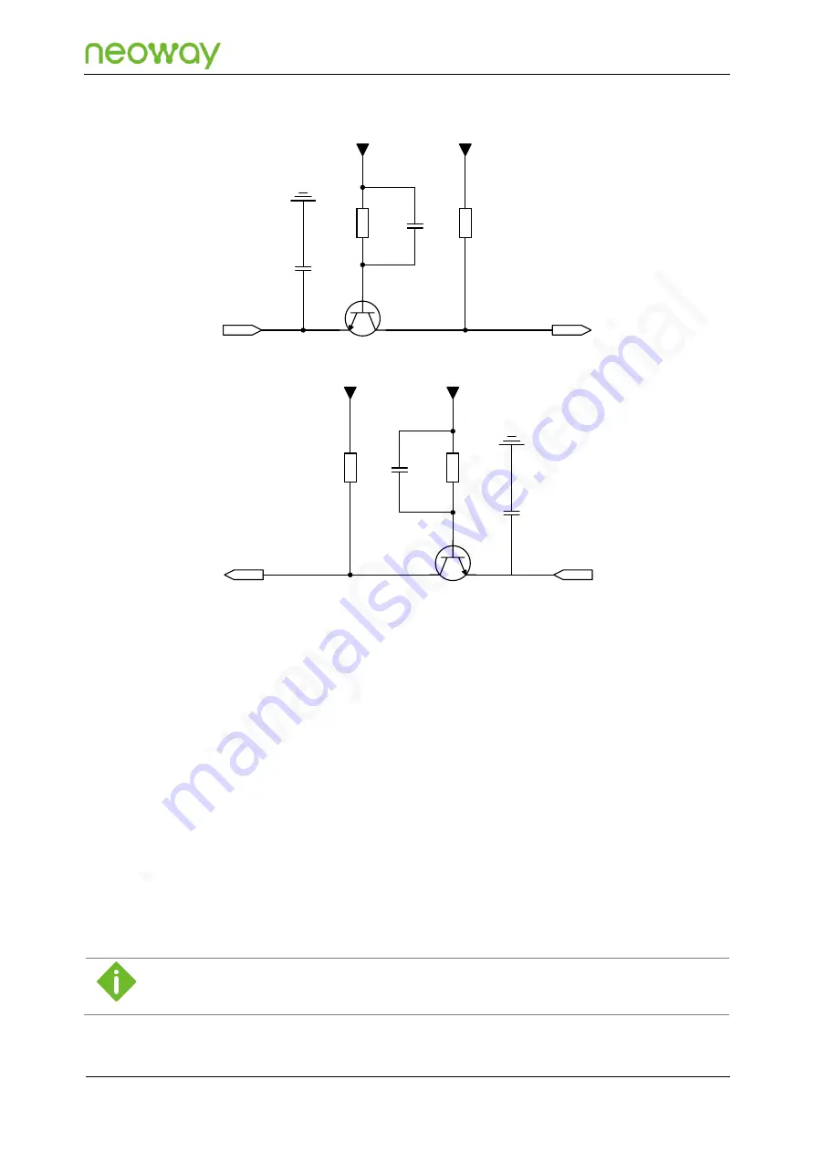
Figure 5-22
Recommended level shifting circuit 3
Q1
4.7k
Ω
R2
10k
Ω
R3
MCU_CTS
VDD_1P8
VCC_IO
UART_RTS
Q2
4.7k
Ω
R4
10k
Ω
R1
UART_CTS
VDD_1P8
VDD_1P8
MCU_RTS
10pF
C1
10pF
C2
10pF
C3
10pF
C4
MCU_CTS and MCU_RTS are the MCU-side signals; UART_CTS and UART_RTS are the module-
side signals. VCC_IO is the IO voltage of the MCU. VDD_1P8 is the IO voltage of the module.
Schematic Design Guidelines:
⚫
Ensure that the voltage difference between the high-level and low-level sides be equal to or less
than 2 V.
⚫
For the accelerating capacitor, adjust it according to the actual test conditions; it is
recommended to reserve the capacitor.
⚫
The base voltage of the transistor is the lower voltage between both sides.
⚫
The circuit convert the voltage level through the turn-on and turn-off of the triode, and the level
conversion is unidirectional. Pay attention to the signal flow.
Do Not directly apply the voltage and resistance values in the circuit to your circuit design; they need to be
adjusted according to the actual situations. Note the difference between different level shifting circuits.


