background image

Chapter 3

Hardware Overview

©

 National Instruments Corporation

3-3

NI PXI-6653 User Manual

NI 6653 Front Panel

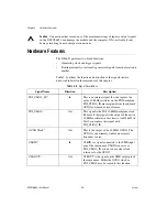
Figure 3-2 shows the connectors and LEDs on the front panel of the 
NI 6653.

Figure 3-2.  

NI 6653 Front Panel

1

Access LED

2

Active LED

3

CLKOUT Connector

4

CLKIN Connector

5

PFI <0..5> Connectors

NI PXI-6653

Timing Module

CLK

OUT

PFI 0

PFI 1

PFI 2

PFI 3

PFI 4

PFI 5

CLK

IN

ACCESS

ACTIVE

1

2

3

4

5

Summary of Contents for PXI-6653

Page 1: ...PXI NI PXI 6653 User Manual Timing and Synchronization Module for PXI NI PXI 6653 User Manual January 2003 Edition Part Number 323388A 01...

Page 2: ...4 Germany 49 0 89 741 31 30 Greece 30 2 10 42 96 427 Hong Kong 2645 3186 India 91 80 4190000 Israel 972 0 3 6393737 Italy 39 02 413091 Japan 81 3 5472 2970 Korea 82 02 3451 3400 Malaysia 603 9059 6711...

Page 3: ...maintenance instructions owner s modification of the product owner s abuse misuse or negligent acts and power failure or surges fire flood accident actions of third parties or other events outside rea...

Page 4: ...eral Communications Commission This equipment has been tested and found to comply with the limits for a Class A digital device pursuant to part 15 of the FCC Rules These limits are designed to provide...

Page 5: ...alling and Configuring Installing the Software 2 1 Installing the Hardware 2 1 Configuring the Module 2 2 Chapter 3 Hardware Overview NI 6653 Front Panel 3 3 Access LED 3 4 Active LED 3 4 Connectors 3...

Page 6: ...erating a Single Pulse Global SoftwareTrigger 3 18 Using the PXI_CLK10 PLL 3 18 Chapter 4 Calibration Factory Calibration 4 1 OCXO Frequency 4 1 PXI_CLK10 Phase 4 1 DDS Start Trigger Phase 4 1 DDS Ini...

Page 7: ...gh nested menu items and dialog box options to a final action The sequence File Page Setup Options directs you to pull down the File menu select the Page Setup item and select Options from the last di...

Page 8: ...ctrical and software features The PXIbus standard was originally developed by National Instruments in 1997 and is now managed by the PXIbus Systems Alliance National Instruments Documentation The NI P...

Page 9: ...ead this manual PICMG 2 0 R3 0 CompactPCI Core Specification available from PICMG available from www picmg org PXI Specification Revision 2 0 available from www pxisa org NI VISA User Manual available...

Page 10: ...the NI 6653 you need the following items NI PXI 6653 Timing and Triggering Module NI PXI 6653 User Manual NI VISA NI PXI 6653 Driver and Examples CD One of the following software packages and document...

Page 11: ...s or any sign of damage Notify NI if the module appears damaged in any way Do not install a damaged module into the computer Store the NI 6653 in the antistatic envelope when not in use Software Progr...

Page 12: ...nmetallic brush The product must be completely dry and free from contaminants before you return it to service Operate the product only at or below Pollution Degree 2 Pollution is foreign matter in a s...

Page 13: ...as that provided by a standard wall outlet for example 115 V for U S or 230 V for Europe Examples of Installation Category II are measurements performed on household appliances portable tools and sim...

Page 14: ...nings about installing new modules 1 Power off and unplug the chassis 2 Choose an available PXI slot in the PXI chassis Note The NI 6653 is usually installed in Slot 2 3 Remove the filler panel for th...

Page 15: ...ware automatically allocates all module resources including base memory address and interrupt level The two LEDs on the front panel provide information about module status The NI 6653 Front Panel sect...

Page 16: ...nstruments Corporation 3 1 NI PXI 6653 User Manual 3 Hardware Overview This chapter presents an overview of the hardware functions of the NI 6653 Figure 3 1 provides a functional overview of the NI 66...

Page 17: ...CLKOUT DDS CLKIN AC Coupled Clock Detector PLL OCXO PXI_CLK10_IN OCXO Calibration DAC OCXO Clock PXI_CLK10 DDS Clock PFI 0 1 Threshold DAC PFI 0 Driver Comparator PFI 1 Driver Comparator PFI 2 Driver...

Page 18: ...nt Panel Figure 3 2 shows the connectors and LEDs on the front panel of the NI 6653 Figure 3 2 NI 6653 Front Panel 1 Access LED 2 Active LED 3 CLKOUT Connector 4 CLKIN Connector 5 PFI 0 5 Connectors N...

Page 19: ...rrides the selection Refer to Figure 3 2 for the location of the Active LED Tip Changing the Active LED color to amber is helpful when you want to identify devices in a multichassis situation or when...

Page 20: ...be routed from the oven controlled crystal oscillator OCXO Direct Digital Synthesis DDS or backplane clock PXI_CLK10 PFI 0 5 Programmable Function Interface 0 5 These connectors can be used for either...

Page 21: ...ction Description PXI_CLK10_IN1 In This is an internal signal that can replace the native 10 MHz oscillator on the PXI backplane PXI_CLK10_IN may originate from the onboard OCXO or from an external so...

Page 22: ...matically phase locks to PXI_CLK10 PXI_STAR 0 12 In Out The PXI star trigger bus connects Slot 2 to Slot 3 15 in a star configuration The electrical paths of each star line are closely matched to mini...

Page 23: ...with the specified frequency You can specify the programmable DDS frequency on the NI 6653 with a precision of better than 1 Hz within the range 1 Hz 80 MHz The accuracy of the frequency depends on t...

Page 24: ...to the CLKOUT connector1 In addition to replacing the native backplane clock directly the OCXO can phase lock to an external frequency source This operation is discussed in detail in the Using the PXI...

Page 25: ...itry PFI 0 PFI 1 PFI 5 Selection Circuitry Selection Circuitry PXI_STAR 0 PXI_STAR 1 PXI_STAR 12 Selection Circuitry Selection Circuitry Selection Circuitry PXI_TRIG 0 PXI_TRIG 1 PXI_TRIG 7 Selection...

Page 26: ...ing Table 3 4 summarizes the sources and destinations of the NI 6653 The destinations are listed in the horizontal heading row and the sources are listed in the column at the far left A in a cell indi...

Page 27: ...panel PFI outputs Using Front Panel PFIs As Outputs The front panel PFI outputs are 3 3 V drivers with 50 output impedance The outputs can drive 50 loads such as a 50 coaxial cable with a 50 receiver...

Page 28: ...rigger 0 is the same for Slot 2 as it is for Slot 3 and so on This feature makes the PXI RTSI triggers convenient in situations where you want for instance to start an acquisition on several devices a...

Page 29: ...rs per chassis Each trigger line is a dedicated connection between Slot 2 and one other slot The PXI Specification Revision 2 0 requires that the propagation delay along each star trigger lines be mat...

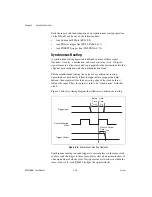
Page 30: ...he destination after a propagation delay through the module Figure 3 5 illustrates an asynchronous routing operation Figure 3 5 Asynchronous Routing Operation Some delay is always associated with an a...

Page 31: ...ke asynchronous routing the output of a synchronous routing operation does not directly follow the input after a propagation delay Instead the output waits for the next rising edge of the clock before...

Page 32: ...ination signal can be inverted which is useful when handling active low digital signals Possible sources for synchronous routing include the following sources Any front panel PFI pin Any PXI star trig...

Page 33: ...ace PXI_CLK10 with the OCXO output This oscillator is a more stable and accurate reference than the native backplane clock The second option is to route a 10 MHz clock directly from the front panel to...

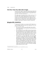
Page 34: ...ck the chassis to it If CLKIN stops or becomes disconnected PXI_CLK10 is still present in the chassis If CLKIN is 10 MHz the NI 6653 can compensate for distribution delays in the backplane The feedbac...

Page 35: ...alculating and storing four calibration constants These values control the accuracy of four features of the device which are discussed in the following sections OCXO Frequency The OCXO frequency can b...

Page 36: ...phase of the DDS output is adjusted using this constant so that the DDS outputs from multiple NI 6653 modules are aligned User Calibration User calibration of the NI 6653 is currently not supported Re...

Page 37: ...and OCXO 1 5 ppm Jitter added to CLKIN Without PLL 15 psrms With PLL 2 5 psrms Duty cycle distortion of CLKIN without PLL 1 Duty cycle of PLL 45 to 55 1 CLKIN fundamental frequency can be any multiple...

Page 38: ...ns max High drive 4 5 ns min 7 ns max Maximum recommended 50 loads2 8 low or high drive square or sine 1 The lower limit is load dependent because of the AC coupling This limit is less than 1 MHz for...

Page 39: ...e resolution 20 mV 8 bits Error 40 mV Hysteresis 10 mV Asynchronous delay tpd PFI 0 5 to PXI_TRIG 0 7 output 16 to 23 ns PFI 0 5 to PXI_STAR 0 12 output 11 to 12 5 ns Synchronized trigger input setup...

Page 40: ...400 ps3 Asynchronous delays tpd PXI_STAR 0 12 to PFI 0 5 output 7 5 to 13 ns PXI_STAR 0 12 to PXI_TRIG 0 7 output 13 to 19 ns PXI Trigger Characteristics Asynchronous delay tpd PXI_TRIG 0 7 to PFI 0...

Page 41: ...lution 711 nHz Frequency accuracy Equivalent to PXI_CLK10 accuracy3 Physical Chassis requirement One 3U CompactPCI or PXI slot PXI Slot 2 for full functionality Front panel connectors SMB male 50 Fron...

Page 42: ...XI 6653 meets the requirements of the following standards for safety and electrical equipment for measurement control and laboratory use IEC 61010 1 EN 61010 1 UL 3111 1 CAN CSA C22 2 No 1010 1 Note F...

Page 43: ...netic Compatibility Directive EMC 89 336 EEC Note Refer to the Declaration of Conformity DoC for this product for any additional regulatory compliance information To obtain the DoC for this product cl...

Page 44: ...n forums a measurement glossary and so on Assisted Support Options Contact NI engineers and other measurement and automation professionals by visiting ni com ask Our online system helps you define you...

Page 45: ...m calibration If you searched ni com and could not find the answers you need contact your local office or NI corporate headquarters Phone numbers for our worldwide offices are listed at the front of t...

Page 46: ...milli 10 3 k kilo 103 M mega 106 Symbols percent plus or minus positive of or plus negative of or minus per degree ohm A accumulator a part where numbers are totaled or stored ADE application developm...

Page 47: ...PXI_CLK10_IN or be used as a phase lock reference for the OCXO CLKOUT CLKOUT is the signal on the SMB output pin of the same name Either the OCXO clock or PXI_CLK10 may be routed to CLKOUT clock hardw...

Page 48: ...ostatic discharge F frequency the basic unit of rate measured in events or oscillations per second using a frequency counter or spectrum analyzer Frequency is the reciprocal of the period of a signal...

Page 49: ...ed frequency signal An oscillator most often generates signals by using oscillating crystals but may also use tuned networks lasers or atomic clock sources The most important specifications on oscilla...

Page 50: ...t R RTSI bus Real Time System Integration bus the NI timing bus that connects DAQ devices directly by means of connectors on top of the devices for precise synchronization of functions S s seconds ske...

Page 51: ...tCtoQ clock to output time thold hold time tpd propagation delay time TRIG trigger signal trigger a digital signal that starts or times a hardware event e g starting a data acquisition operation tset...

Page 52: ...ription 3 5 location diagram 3 3 signal description table 3 6 specifications A 2 clock generation DDS 3 8 overview 3 7 PXI_CLK10 and OCXO 3 8 color Access LED color explanation table 3 4 Active LED co...

Page 53: ...as outputs 3 12 G generating a clock DDS 3 8 overview 3 7 PXI_CLK10 and OCXO 3 8 generating a single pulse trigger 3 18 getting started configuring the device 2 2 equipment 1 1 installing the hardware...

Page 54: ...crystal oscillator See OCXO P PFI PFI 0 5 connector description 3 5 location diagram 3 3 signal description table 3 7 PFI 0 5 signals asynchronous routing 3 16 front panel PFIs as inputs 3 12 front pa...

Page 55: ...10 routing signals front panel triggers using as inputs 3 12 using as outputs 3 12 generating a single pulse trigger 3 18 overview 3 9 possible sources and destinations table 3 11 PXI star triggers 3...

Page 56: ...17 synchronization clock sources 3 17 timing diagram 3 16 system integration services B 1 T technical support B 1 telephone technical support B 2 terminating signals with resistors note 3 12 threshol...

Reviews: