1-10
|
ni.com
Chapter 1
Getting Started
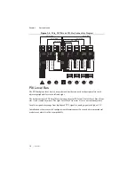
PXI_CLK10, PXIe_CLK100 and PXIe_SYNC100 have the default timing relationship
described in Figure 1-6.
Figure 1-6.
System Reference Clock Default Behavior
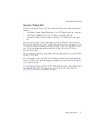
To synchronize the system to an external clock, you can drive PXI_CLK10 from an external
source through the PXI_CLK10_IN pin on the System Timing Slot. Refer to Table B-7,
Connector Pinout for the System Timing Slot
, for the pinout. When a 10 MHz clock is detected
on this pin, the backplane automatically phase-locks the PXI_CLK10, PXIe_CLK100, and
PXIe_SYNC100 signals to this external clock and distributes these signals to the slots. Refer to
Appendix A,
, for the specification information for an external clock provided on
the PXI_CLK10_IN pin of the system timing slot.
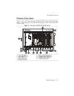
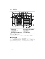
You also can drive a 10 MHz clock on the 10 MHz REF IN connector on the rear of the chassis.
Refer to Figure 1-2 for the location of this connector. When a 10 MHz clock is detected on this
connector, the backplane automatically phase-locks the PXI_CLK10, PXIe_CLK100, and
PXIe_SYNC100 signals to this external clock and distributes these signals to the slots. Refer to
Appendix A,
, for the specification information for an external clock provided on
the 10 MHz REF IN connector on the rear panel of the chassis.
If the 10 MHz clock is present on both the PXI_CLK10_IN pin of the System Timing Slot and
the 10 MHz REF IN connector on the rear of the chassis, the signal on the System Timing Slot
is selected. Refer to Table 1-1 which explains how the 10 MHz clocks are selected by the
backplane.
Table 1-1.
Backplane External Clock Input Truth Table
System Timing Slot
PXI_CLK10_IN
Rear Chassis Panel
10 MHz REF IN
Backplane PXI_CLK10,
PXIe_CLK100 and PXIe_SYNC100
No clock present
No clock present
Backplane generates its own clocks
No clock present
10 MHz clock present
PXI_CLK10, PXIe_CLK100 and
PXIe_SYNC100 all phase-locked to
Rear Chassis Panel—10 MHz REF IN
PXIe_CLK100
PXI_CLK10
PXIe_
S
YNC100
0 1 2
3
4 5 6 7
8
9 0 1 2
3
4 5 6 7
8
9 0 1 2
3
4 5 6 7
8
9

