JAA63051-R.3689.A
- T4・ AF-S VR MC 105/2.8G -
GND
VCC (5.0V)
MR-A
MR-B
③
Solder the three wires on the pattern of
the front-side PCB.
④
Solder the one wire on the pattern of the
back-side PCB.
PCB (Front)
PCB (Back)
● To inspect and adjust the output waveform of MR encoder, it is necessary to make a self-made tool by using
the RP main PCB (IS020-426) of AF-SVR18-200. (If there is a defective main PCB after replacements/
repairs, use the defective one.)
Make a self-made tool according to the following procedure.
Making of Self-made Tool
Main PCB
Use this range.
Connector
①
Remove the mounted parts/elements (condenser,
transistor, IC, etc.) from the both faces of the
PCB within the range of the dotted lines. (See
the left.) Do not remove the connector.
(The parts/elements are not always needed to
be removed, if they are not affected by the next
cutoff or soldering.)
②
Cut off the PCB along the dotted lines.
Summary of Contents for AF-S VR Micro Nikkor 105mm/f2.8G
Page 13: ...JAA63051 R 3689 A D11 AF S VR MC 105 2 8G Focus index unit 83 3 GMR unit Focus index unit ...
Page 100: ...JAA63051 R 3689 A A76 AF S VR MC 105 2 8G Target chart Resolution chart ...
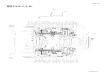
Page 107: ...JAA63051 R 3689 A F1 AF S VR MC 105 2 8G 外観図 Sketch drawings ...
Page 108: ...JAA63051 R 3689 A F2 AF S VR MC 105 2 8G 組立図 Structure of the Lens ...
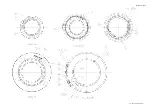
Page 109: ...JAA63051 R 3689 A F3 AF S VR MC 105 2 8G ...
Page 110: ...JAA63051 R 3689 A F4 AF S VR MC 105 2 8G ...
Page 111: ...JAA63051 R 3689 A F5 AF S VR MC 105 2 8G ...
Page 112: ...JAA63051 R 3689 A F6 AF S VR MC 105 2 8G ...
Page 113: ...JAA63051 R 3689 A F7 AF S VR MC 105 2 8G ...


