After Sales
Technical Documentation
RAE/RAK–1N
UIF
Page 4– 8
Amendment 1 04/97
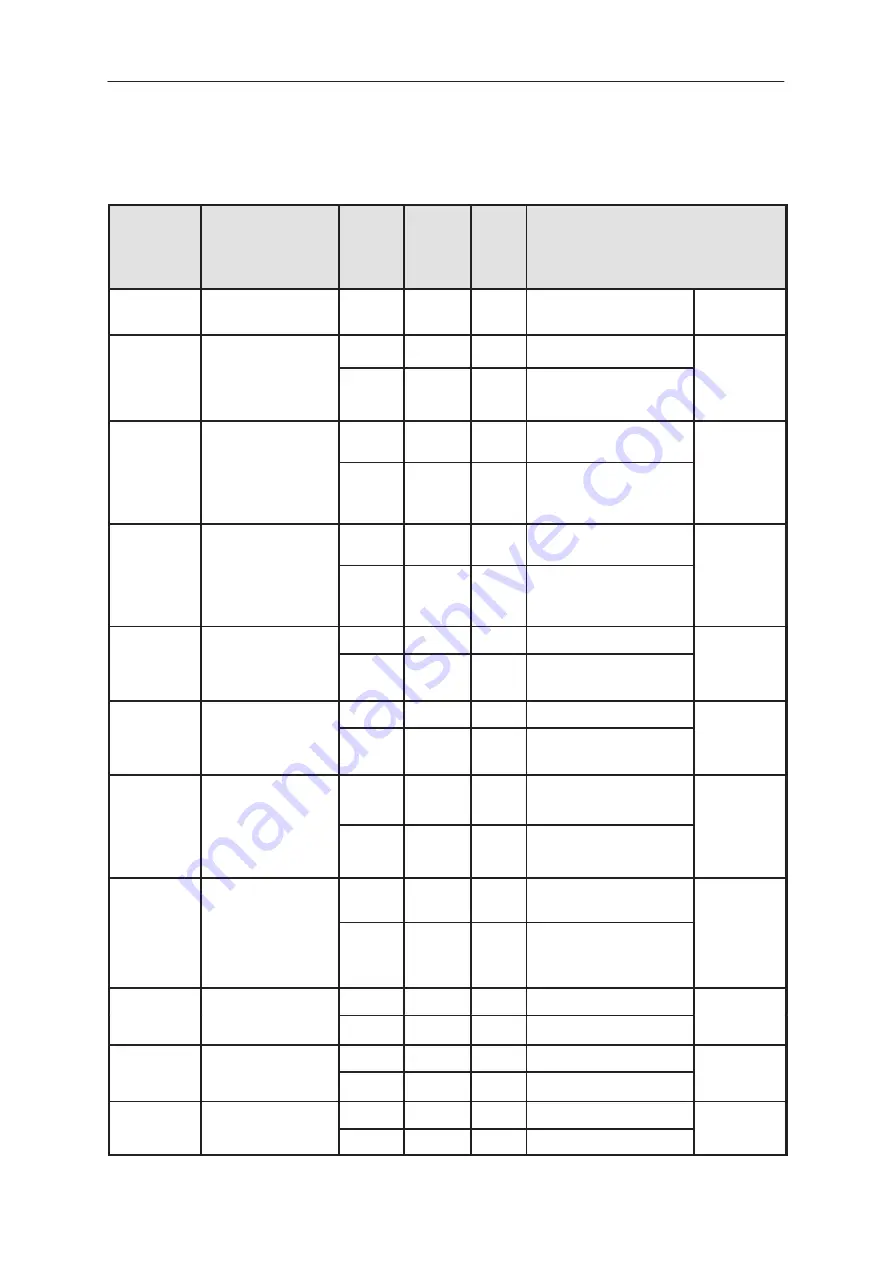
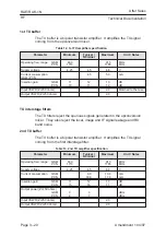
Table 2. DC characteristics of PDA Hinge–flex connector on LCDM module
Pin /
Type
Line Symbol
Mini-
mum
Typi-
cal /
Nomi-
nal
Maxi-
mum
Notes
10,17,24 /
UIF
GND
GND
6–3 / UIF
LCMUIF(3:0)
0V
0.7V
Output/Input low
keypad
row lines/
4.65V
4.8V
4.95
V
Output/Input high
row lines/
display
data lines
7 / UIF
LCMUIF4
0V
0.7V
Output/Input low
keypad
row
4.65V
4.8V
4.95
V
Output/Input high
read/write
strobe for
LCD driver
8 / UIF
LCMUIF5
0V
0.7V
Output/Input low
keypad
row
4.65V
4.8V
4.95
V
Output/Input high
LCD driver
register
select
9 / UIF
LCMUIF6
0V
0.7V
Output/Input low
enable
t b f
4.65V
4.8V
4.95
V
Output/Input high
strobe for
LCD driver
14–11 /
UIF
LCMCOL(3:0)
0V
0.7V
Output/Input low
Keypad
l
UIF
4.65V
4.8V
4.95
V
Output/Input high
column
write
15 / UIF
BACKLIGHTO
0V
0.7V
Output low, back-
lights off
Display
and key-
pad illu
4.65V
4.8V
4.95
V
Output high, back-
lights on
pad illu-
mination
control
16 / UIF
LCMXPWRON
0V
0V
0.7V
Input low, power on/
off
Power
ON/OFF
k
4.8V
Floating when inac-
tive. A pull–up in
PSL+.
key
21–18 /
PDALCD
LCDD(3:0)
0.4 V
Output low
PDA LCD,
D t li
PDALCD
2.6 V
Output high
Data lines
22 /
PDALCD
LP
0.4 V
Output low
PDA LCD,
Li
l
PDALCD
2.6 V
Output high
Line pulse
23 /
PDALCD
PCLK
0.4 V
Output low
PDA LCD,
Pi
l l
k
PDALCD
2.6 V
Output high
Pixel clock
Summary of Contents for 9000i
Page 7: ...After Sales Technical Documentation RAE RAK 1N Series Original 08 96 Chapter 1 Overview ...
Page 287: ...After Sales Technical Documentation RAE RAK 1N Series Original 08 96 Chapter 9 Service Tools ...
Page 301: ...After Sales Technical Documentation RAE 1N Series Original 04 97 Chapter 10 Schematics ...
Page 303: ...RAE 1N Original 08 96 10 11 Page 1 Figure 1 Component Layout Bottom ...
Page 304: ...RAE 1N Original 08 96 10 12 Page Figure 2 Component Layout Top ...
Page 305: ...RAE 1N Original 08 96 10 13 Page Figure 3 Baseband Circuit Diagram PWRU ...
Page 306: ...RAE 1N Original 08 96 10 14 Page Figure 4 Baseband Circuit Diagram MCM1 ...
Page 307: ...RAE 1N Original 08 96 10 15 Page Figure 5 Baseband Circuit Diagram MCM2 ...
Page 308: ...RAE 1N Original 08 96 10 16 Page Figure 6 RF TX Circuit Diagram ...
Page 309: ...RAE 1N Original 08 96 10 17 Page Figure 7 RF RX Circuit Diagram ...
Page 310: ...RAK 1N 10 20 Page Amendment 1 04 97 Figure 18 PCN Component Layout Bottom ...
Page 311: ...RAK 1N 10 21 Page Amendment 1 04 97 Figure 19 PCN Component Layout Top ...
Page 312: ...RAK 1N 10 22 Page Amendment 1 04 97 Figure 20 PCN RF TX ...
Page 313: ...RAK 1N 10 23 Page Amendment 1 04 97 Figure 21 PCN RF RX ...
Page 314: ...RAK 1N 10 24 Page Amendment 1 04 97 Figure 22 UIF Schematic PCN ...
Page 315: ...RAK 1N 10 25 Page Amendment 1 04 97 Figure 23 UIF Component Layout PCN ...
Page 316: ...RAE 1N Original 05 97 10 3 Page Figure 1 PDA Block Diagram Edit 82 for layout 13a ...
Page 317: ...RAE 1N Original 05 97 10 4 Page Figure 2 PDA Power Unit PWRU Edit 108 for layout 13a ...
Page 318: ...RAE 1N Original 05 97 10 5 Page Figure 3 PDA Serial Interface SIRU Edit 24 for layout 13a ...
Page 319: ...RAE 1N Original 05 97 10 6 Page Figure 4 PDA MCU and Memory PROCU Edit 121 for layout 13a ...
Page 320: ...RAE 1N Original 05 97 10 7 Page Figure 5 PDA EMIU Edit 21 for layout 13a ...
Page 321: ...RAE 1N Original 05 97 10 8 Page Figure 6 Keyboard matrix Edit 24 for layout 13a ...
Page 322: ...RAE 1N Original 05 97 10 9 Page Figure 7 PDA Memory Edit 28 for layout 13a ...
Page 323: ...RAE 1N Original 05 97 10 10 Page Figure 8 PDA Component Layout 13a ...
Page 324: ...RAE 1N Original 08 96 10 18 Page Figure 1 UIF Schematic ...
Page 325: ...RAE 1N Original 08 96 10 19 Page Figure 2 Component Layout Uif ...
Page 326: ...After Sales Technical Documentation RAE RAK 1N Series Original 08 96 Accessories ...
Page 352: ...After Sales Technical Documentation Appendix 2 RAE RAK 1N Amendment 1 04 97 PARTS LISTS ...
Page 402: ...After Sales Technical Documentation Appendix 1 RAE RAK 1N Original 08 96 QUICK GUIDE ...
Page 434: ......


