background image

RM-12 

Nokia Customer Care

Issue 1  11/2004

COMPANY CONFIDENTIAL

61

Copyright © 2004 Nokia. All Rights Reserved.

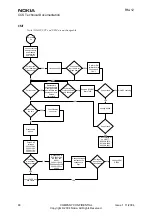
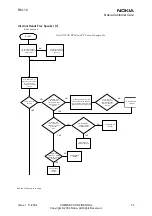
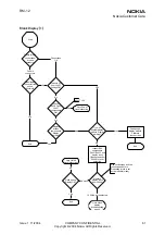
Blank Display (1)

Inspect EMI

components

Z4421-Z4423 and

display clock

filtering capacitor

C4444 for poor

soldering.

Check for bad

connections/

broken

connector.

Fault in

connectors

Connections

OK

Yes

Clean/replace

connector from

phone.

Working?

Try with

another display
module. Display

working?

Yes

No

12.5MHz clock detected

Measure V28

from L4427.

Voltage OK?

Measure

display clock

from C4444.

No clock

No

End

Yes

Go to Power

troubleshooting

No

Check

C4439-C4440,

L4427

components

OK?

No

Yes

Replace

broken

components.

Display

working?

No

Yes

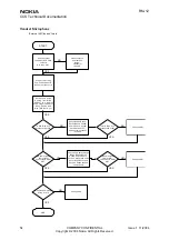
Go to blank

display

troubleshooting

page 2

Use oscilloscope and tap
touchscreen before
measuring (clock is not
active in partial mode)

Start

End

Change new

display module.

Calibrate

touchscreen

Goto OMAP

troubleshooting

L4427 = 0V

Flash phone.

Display OK?

No

End

Yes

Summary of Contents for RM-12

Page 1: ...Issue 1 11 2004 COMPANY CONFIDENTIAL 1 Copyright 2004 Nokia All Rights Reserved Customer Care Solutions Technical Documentation 6 Troubleshooting Instructions ...

Page 2: ...RM 12 CCS Technical Documentation 2 COMPANY CONFIDENTIAL Issue 1 11 2004 Copyright 2004 Nokia All Rights Reserved This page intentionally blank ...

Page 3: ...evice 33 Most common symptoms reported by customer 33 Dead or jammed device troubleshooting 35 ASIC is changed 40 Test points 40 Selftests Contact service on display 40 Flashing troubleshooting 44 Power troubleshooting 47 Audio troubleshooting 53 Display troubleshooting 60 Pixel defects 65 Backlight troubleshooting 1 67 Backlight troubleshooting 2 68 Backlight troubleshooting 3 69 Hall sensor trou...

Page 4: ...idea whether the device is able to start up Dropping supply voltage or very large current consumption indicates a short circuit Check whether the connection with Phoenix works and what can be discovered with Phoenix ADC readings baseband selftest bb calibrations etc Check display keyboard and rocker faults visually Force phone to LOCAL mode and make keyboard test by Phoenix NOTE If liquid damage s...

Page 5: ... straps and ESD soldering irons HELGO and PA are moisture sensitive so parts must be pre baked prior to soldering Apart from key components described in this document here are a lot of discrete components resistors inductors and capacitors the troubleshooting of which is done by checking if solder ing of the component is done properly for factory repairs checking if it is missing from PWB Capacito...

Page 6: ... Copyright 2004 Nokia All Rights Reserved RF Key component placement Figure 1 Component placement 1 Helgo86 RF ASIC 4GHz VCO Antenna Switch Module 900 RX SAW 1900 LNA 1900 RX balun 1800 RX SAW Power Amplifier 900 TX SAW 26 MHz VCTCXO VCO balun 1800 1900 TX balun 1900 RX SAW ...

Page 7: ...900RX ASM_out_1800RX ASM_out_900RX ASM_in_1800 1900TX VANT_2 VANT_1 ASM_in_900TX Iref_900 To antenna PA_in_900 VTXB_900 VPCTRL_900 VPCTRL_1800 1900 VTXB _1800_1900 PA_in_1800 1900 VR2 VR3 VCTCXO 26Mhz out VR1 TXIN TXIP TXQP QN TXP J7300 VR5 TXA J7301 TXC VR6 VR7 VR4 900_RX_In 1800_RX_In 1900_RX_In RFBusEna1 J7306 VPECTRL3 ALC RXQ J7303 RXI J7302 RFBusReset J7307 RFBusData J7304 RFBusClk J7305 26MH...

Page 8: ...erwise the PA may be damaged Normally a spectrum analyzer is used as measurement equipment NOTE Normally Spectrum analyzer maximum input power is 30dBm It is recommended to use 10dB attenuator on Spectrum analyzer input to prevent damage Set the phone module to test jig and start Phoenix service sofware Initialize connection to phone Use FBUS driver when using DAU9S COMBOX driver when using FPS 8 ...

Page 9: ...Check output signal on 500MHz span Signal found on incorrect frequency Synthesizer troubleshooting Check with RF probe signal level on PA input 1 5dBm OK Helgo troubleshooting Start TX power level tuning and check tuned coefficient values Highest level 0 655 0 831 GSM900 0 567 0 782 GSM1800 1900 Lowest level 0 166 0 196 GSM900 0 176 0 225 GSM1800 1900 Base level 0 137 0 166 GSM900 0 132 0 161 GSM1...

Page 10: ...C troubleshooting Check with oscilloscope TXI TXQ signals VR1 VR2 VR4 VR5 VR6 2 8V VrefRF01 1 35V Helgo serial interface TXP TXC signals OK Baseband troubleshooting Check with RF probe 4G VCO signal output 3589 6MHz GSM900 3495 6MHz GSM1800 3760MHz GSM1900 Level 10dBm OK Synthesizer troubleshooting Check modulator output components OK Replace HELGO Replace faulty component s ...

Page 11: ...s No PA Antenna Switch troubleshooting Check with RF probe signal level on PA input 1 5 dBm OK Check with oscilloscope VANT1 GSM900 VANT2 GSM1800 VANT3 GSM1900 OK Replace ant switch Check with oscilloscope VBATT 4V VTXB 2 8V pulsed VPCTRL_900 1800 1900 OK Check VANT line components OK Replace PA Replace HELGO Replace faulty component s Check components around PA OK Replace faulty component s ...

Page 12: ...ight 2004 Nokia All Rights Reserved Pictures of transmitter signals Figure 6 Transmitter signals VPCTRL Figure 7 Transmitter signals TX I Q at R7304 7305 power level high Random data VPCTRL900 power level high at R7003 VPCTRL1800 1900 power level high at R7007 200mV div 100us div ...

Page 13: ...2004 Nokia All Rights Reserved VANT_1 GSM900 TX at C7100 VANT_2 GSM1800 TX at C7102 VANT_3 GSM1900 TX at C7101 OV no signal Flatline on Oscilloscope screen VTXB_900 at C7013 VTXB_1800_1900 at C7014 TXC at R7303 TXP at J7300 500mV div 100us div 500mV div 100us div 1 500mV div 100us div ...

Page 14: ... see GSM900 1800 1900 troubleshooting instruc tions Select product from the menu File Choose Product RM 12 From toolbar set operating mode to Local Activate RF controls window from the menu Testing RF Controls From the RF controls window Select Band GSM900 or GSM1800 or GSM1900 Default GSM900 A Unit dBm 1MA 21 dB Offset Ref Lvl 34 dBm Ref Lvl 34 dBm RF Att 40 dB Center 897 4 MHz Span 2 MHz 200 kHz...

Page 15: ... Set Operation mode to Burst Default Burst Set Tx data type to Alternate PN9 Default All1 Set Rx Tx channel to 37 on GSM900 or 700 on GSM1800 or 661 on GSM1900 Defaults Set power level to 8 Default 19 on GSM900 or to 2 Default 15 on GSM1800 or GSM1900 NOTE For GSM900 Edge power levels 5 6 and 7 are not in use and for GSM1800 1900 Edge power levels 0 and 1 are not in use ...

Page 16: ...t frequency Synthesizer troubleshooting Check with RF probe signal level on PA input 8dBm PCL 8 GSM900 10dBm PCL 2 GSM1800 1900 OK Helgo EDGE troubleshooting Start TX Edge power level tuning and check tuned coefficient values Highest level 0 684 0 841 GSM900 0 763 0 860 GSM1800 1900 Lowest level 0 333 0 420 GSM900 0 323 0 362 GSM1800 1900 Base level 0 273 0 313 GSM900 0 244 0 313 GSM1800 1900 Majo...

Page 17: ...ubleshooting Check with oscilloscope TXI TXQ signals VR1 VR2 VR4 VR5 VR6 2 8V VrefRF01 1 35V Helgo serial interface TXP TXC TXA OK Baseband troubleshooting Check with RF probe 4G VCO signal output 3589 6MHz GSM900 3495 6MHz GSM1800 3760MHz GSM1900 Level 10dBm OK Synthesizer troubleshooting Check modulator output components and VPECTRL3 signal OK Replace HELGO Replace faulty component s ...

Page 18: ...ting Check with RF probe signal level on PA input 8dBm PCL 8 GSM900 10dBm PCL 2 GSM1800 1900 OK Check with oscilloscope VANT1 GSM900 VANT2 GSM1800 VANT3 GSM1900 OK Replace ant switch Check with oscilloscope VBATT 4V Iref _900 2V peak Iref_1800_1900 2 1V peak VTXB 2 8V pulsed Mode 1 8V OK Check VANT line components OK Replace PA Replace HELGO Replace faulty component s Check components around PA OK...

Page 19: ...Documentation 17 COMPANY CONFIDENTIAL Issue 1 11 2004 Copyright 2004 Nokia All Rights Reserved Pictures of EDGE transmitter signals Figure 12 I_ref_900 power level 8 at R7019 C7001 Figure 13 VTXB 900 power level 8 at C7013 ...

Page 20: ...S Technical Documentation Issue 1 11 2004 COMPANY CONFIDENTIAL 18 Copyright 2004 Nokia All Rights Reserved Figure 14 I_ref_1800 1900 power level 2 at R7017 C7000 Figure 15 VTXB 1800 1900 power level 2 at C7014 ...

Page 21: ...Figure 16 TXA 900 1800 1900 at C7309 Figure 17 TXI TXQ signal at C7311 C7312 R7304 R7305 ...

Page 22: ...Figure 18 VPECTRL3 ALC signal at C7309 ...

Page 23: ... Use FBUS driver when using DAU 9S COMBOX driver when using FPS 8 Choose product from the menu File Choose product RM 12 From toolbar set operating mode to Local Activate RF controls window from the menu Testing RF Controls From the RF controls window Select band GSM900 GSM 1800 or GSM1900 Default GSM900 Set Active unit to Rx Default Rx Set Operation mode to Burst Default Burst For continuous mode...

Page 24: ...r Figure 1 RX I Q signal burst mode input level 90dBm Receiver I or Q burst mode signal channel 37 measured from testpoint RXI or RXQ with 942 46771 MHz signal input level 90dBm at RF connector Correct signal amplitudes approximately GSM900 170mVpp GSM1800 140mVpp GSM1900 160mVpp Signal part frequency 67 7kHz sine DC level of signal part is 1 35V DC level can variate about 100mV between I and Q si...

Page 25: ... mode GSM1900 receiver burst mode I or Q signal at ch 661 with input signal 1960 067MHz level 90 dBm at RF connector Trace2 With wider time scaling both monitoring and own RX bursts are seen 1st burst shorter is monitoring and 2nd burst longer is own RX burst Trace1 External LNA VCC supply voltage at burst mode input level 90 dBm Measured from testpoint LNA_VCC ...

Page 26: ...3 RX I Q phase difference 90 deg between signals Detailed view of GSM900 continuous mode RX I and Q signals measured from testpoints RXI and RXQ simultaneously Used channel 37 input signal 942 46771 MHz level 90 dBm at antenna port AGC setting 12 Phase difference should be 90 degrees between RX I and Q signals at all bands ...

Page 27: ...loscope Check HELGO serial interface burst mode Oscilloscope VR1 3 6 2 7V Check HELGO serial interface burst mode Spectrumanalyzer reading with 1 kohm passive probe right value add 26dB All spectrumanalyzer reading values are measured with 1 kohm passive probe use tweezers to connect the probe ground to the nearest PWB ground Reading value is represented without 26 dB compensation Spectrumanalyzer...

Page 28: ...trumanalyzer reading with 1 kohm passive probe right value add 26dB All spectrumanalyzer reading values are measured with 1 kohm passive probe use tweezers to connect the probe ground to the nearest PWB ground Reading value is represented without 26 dB compensation Spectrumanalyzer 4G VCO output 3685 6MHz 30dBm Check HELGO N500 Check Baseband Check C809 Rx 1800 chain functional Check Z808 L838 L83...

Page 29: ...sive probe right value add 26dB All spectrumanalyzer reading values are measured with 1 kohm passive probe use tweezers to connect the probe ground to the nearest PWB ground Reading value is represented without 26 dB compensation Spectrumanalyzer 4G VCO output 3920 MHz 30dBm Check HELGO N500 Check Baseband Check C809 Rx 1900 chain functional Check Z806 Check Baseband Synthesizer troubleshooting Ch...

Page 30: ...PCS 1 cable Set the DC supply voltage to 4 2V Set the phone module to test jig and start Phoenix service sofware Initialize connection to phone Use FBUS driver when using DAU9S COMBOX driver when using FPS 8 Select product from the menu File Choose product RM 12 From toolbar set operating mode to Local Activate RF controls window from the menu Testing RF Controls From the RF controls window Select...

Page 31: ... RF probe 4G VCO out signal 3589 6 MHz GSM900 3495 6 MHz GSM1800 3760 MHz GSM1900 Level 10dBm OK VCO out signal level 10dBm Check balun output levels and solder joints OK Check output signal on 1 GHz span Signal found on incorrect frequency Check with oscilloscope 4G VCO Vcc 2 7V OK Baseband troubleshooting Check with oscilloscope Check with oscilloscope VCO control voltage VCO control voltage fro...

Page 32: ...CCS Technical Documentation 30 COMPANY CONFIDENTIAL Issue 1 11 2004 Copyright 2004 Nokia All Rights Reserved Pictures of synthesizer signals Figure 8 26MHz at G7200 pin out Figure 9 26MHz RFCLK at R2902 C2902 ...

Page 33: ...RM 12 CCS Technical Documentation Issue 1 11 2004 COMPANY CONFIDENTIAL 31 Copyright 2004 Nokia All Rights Reserved Figure 10 1800 TX channel 512 burst mode Figure 11 1900 RX channel 810 continuous mode ...

Page 34: ...d demodulated I and Q signals RFBus Data J7304 1 and 0 1 8 0V digital signal data frequency max 10MHz RFBUs data read write RFBusClk J7305 1 and 0 1 8 0V digital signal data frequency max 10MHz RF Bus clock RFBus Ena1 J7306 1 and 0 1 8 0V digital signal RFBus enable RESET J7307 1 and 0 1 8 0V digital signal Reset to Helgo RX Channel Select Filter CalRX Cal RX Band Filter Response Cal RX DtoS Balan...

Page 35: ... service Some tips for locating the problem are also given When troubleshooting use these tips and follow the given troubleshooting path Most common symptoms for audio problems Earpiece sound is missing Handsfree sound is missing Microphone is not working Ringing tones do not work Audio volume too low IHF does not work If the symptom is one of the above see Audio troubleshooting Most common sympto...

Page 36: ...d is not working Rocker is not working Backlight is dim Backlight not even Backlight is blinking Keypad or display backlight is not working Display related problems See UI troubleshooting Most common RF related symptoms Call cannot be made Phone does not find signal Call is often dropped See RF troubleshooting Problems related to camera Bad image quality Picture cannot be taken See Camera module t...

Page 37: ... service battery via ammeter Power On Any image on screen Ammeter 0 mA No No Normal operation Yes Yes Connect PC to Phone using DAU 9S cable Scan product No Yes RM 12 found No Go to OMAP1510 troubleshooting Flash the phone Succeed Yes Go to power troubleshooting No End test Yes Yes Normal operation Go to visit display troubleshooting No Normal operation No Yes ...

Page 38: ...AM troubleshooting APE Power OK fixed problem solved APE clocks reset OK fixed problem solved Yes No Yes Booting problems Visit APE clock troubleshooting Yes No Was it a SDRAM problem Replace OMAP1510 D4800 No End Yes Start End Was it a NAND problem No Yes Go to visit APE NAND troubleshooting Check resistor R4806 replace if needed Problem solved No Yes End engine board ...

Page 39: ...t Incorrect Check and replace if needed C5083 C5089 resistance 1Mohm Correct Incorrect Phone might been dropped solder balls cracked replace D5080 Visit APE Power troubleshooting Incorrect Measure SDRAM voltages V18 at C5083 Correct No Problem occurs only in heat or cold Yes Phone might been dropped solder balls cracked replace D5080 Start All signals in this troubleshooting are in range 0 V18 Use...

Page 40: ...eserved SDRAM 2 Inspect R4808 value approx 22ohm No Replace R4808 and measure SDCLK frequency 70Mhz No Yes Rerun ST_APE_RAM_ TEST with Phoenix Fail Pass Go to OMAP1510 troubleshooting Yes Problem occurs while booting No Yes Go to Seija NAND troubleshooting Change SDRAM D5080 From SDRAM troubleshooting page 1 ...

Page 41: ...ck MDOC I O voltage at C5001 V18 Check MDOC core voltage at C5000 V28 Correct voltages Go to APE Power troubleshooting Voltage levels invalid RSTIN stays low Voltage level invalid Check resistor R4801 10k Yes No Replace resistor R4801 and rerun first test MDOC damaged replace D5000 Check resistors R5000 and R5001 both 10k No Replace damaged resistor s Yes Go to APE reset troubleshooting Measure MP...

Page 42: ... memory is changed User data needs to be back upped if possible Re flash the phone Touch screen controller If touch screen controller or display module is changed calibrations should be made BT If BT chip is changed there is no need to flash the phone Test points Test point locations and possible signal levels are listed in the Schematics chapter of this Serv ice Manual Selftests Contact service o...

Page 43: ...ion tests the connection of SimClk and SimIODa signals between UPP and UEM This test requires also that SimIOCtrl signal can be set to high state ST_SIM_IO_CTRL_LOOP_TEST This function tests the connection of SimIOCtrl and SimIODa signals between UPP and UEM This test requires also that SimClk signal can be switched ST_SLEEP_X_LOOP_TEST This function tests the connection of SleepX and SleepClk sig...

Page 44: ...connection of CBUSCLK CBUSDA and CBUSENX signals between UPP and UEM ST_VIBRA_TEST This test verifies the vibra lines ST_SLEEPCLK_FREQ_TEST Purpose of this test is to check the basic functionality of ST_SLEEPCLK_FREQ_TEST ST_CURRENT_GAUGE_IF_TEST Purpose of this test is to check that ST_CURRENT_GAUGE_IF_TEST is working in real HW environment Test uses current gauge registers to verify that correct...

Page 45: ... of the boot up sequence It is based on the assumption that UART communication is required to successfully run the initiali sation sequence It cannot be assumed that if the connection works if a UART command is sent to the Bluetooth ASIC Therefore the Bluetooth ASIC must send the status information OK Not OK to the test server in the boot sequence ST_XABUS_TEST Purpose of this test is to check tha...

Page 46: ... Rights Reserved Flashing troubleshooting Flashing does not work OK No Check cables and flashing adapter Verify that you have the right data package Check Nokia 7710 flashing instructions From APE flashing troubleshooting From the CMT flashing troubleshooting Go to CMT flashing troubleshooting RM 12 ...

Page 47: ...oubleshooting Phone starts to boot but jams after a while Fail Go to APE power troubleshooting No totally dead device Yes Flashing stalls ADL sending code x x 100 Go to NAND troubleshooting Yes No From the CMT flashing troubleshooting Reflash pass CMT functionality OK and automatically ran self tests passed Go to OMAP1510 troubleshooting Go to CMT troubleshooting Yes No ...

Page 48: ... FBUS and BSI signals while flashing BSI pulse exists during flashing No Check BSI line including X2020 R2035 C2020 R2201 C2225 and R2202 No Is FBUSTX 1 8V during flashing Check R2025 if OK change UEM No Change UPP D2800 Yes IS FBUS TX set LOW after it has been HIGH Yes No Check Phoenix Prommer Tool window information Yes Wrong Manufacturer ID or Device ID Change flash D3000 Yes No Go to APE flash...

Page 49: ...ut name Output voltage Test point Supply to N4201 V15 1 57 C4214 D4800 Omap1510 core N4202 V18 1 8 C4212 D4800 Omap 1510 io D5080 SDRAM D5000 MDOC camera N4200 V28 2 8 C4202 D4800 Omap 1510 io camera con verter display module N4400 touch controller N5200 VMMC 3 C5202 MMC N2000 Vout 2 8 C2000 Pop port N2001 V33 3 3 C2005 D4800 Omap 1510 USB D4420 VLED 10 11V C4424 Backlight keylight ...

Page 50: ...owe RF VBAT filter L7000 Current short Goto RF checking NO Change R2036 YES Any damaged component found and changed YES NO Current short Check CMT voltages C2232 2 8V C2202 2 8V C2204 1 8V C2205 1 5V NO CSP component on VBATT N2000 N2070 N2100 N2200 N4200 N4201 N4202 N5200 YES Current rises over 100mA but drops down Perform EM calibration with Phoenix and JBV 1 YES NO NO Disassemble phone Check CM...

Page 51: ...ttery 75kohm Disassemble phone and check Battery contacts Phone in jig Measure voltage on R2202 Normal mode 1 3V Change R2201 and R2202 NO YES Connect charger and read Vchar voltage by Phoenix ACP 12 5 7V Measure Vchar from fuse F2020 5 7V YES Change fuse F2020 and V2020 NO Charging OK NO Read BSI by Phoenix With servce battery 75kohm Flash phone SW NO NO YES Flash phone SW NO Charging OK Charging...

Page 52: ... Check enable VIO high 1 8V YES UEM fault NO Check voltage at L4201 both sides low 0V Change coil and retestV15 NO YES Change SMPS chip N4201 and retest OK YES Check ref voltage at C4211 1 35V NO YES Check voltage at L4202 both sides low 1V Change coil and retestV18 YES NO Change SMPS chip N4202 and retest OK YES Visit APE reset troubleshooting Change filter L4200 YES Ref voltage found at either e...

Page 53: ...ge UEM Check solder joints of V6031 and replace the component if necessary Change B4800 If this doesn t help change C4800 C4801 and C4802 Fix solder joints 12Mhz clock C4800 OSC1_IN Vpp 1 7V f 12 0MHz Figure 3 Yes Yes SleepClk J2802 Voh 1 8V f 32 768kHz Figure 2 No No Go to CMT clocks troubleshooting Yes Solder joints of C4800 C4801 C4802 and B4800 OK Measure resistanceover C4801 R 1M No Yes Yes N...

Page 54: ...uld be 65 195ms Fig 5 R4802 100k solder joints OK Check completed Check the solder joints of N4800 and change the chip if necessary Fix solder joints or change R4802 Yes No Yes No Switch poweron by connecting power to battery terminals of the phone Low to high transition on PURX N4800 pin 3 Voh 1 8V Fig 5 Yes Go to CMT troubleshooting No Note Only probes having input impedanceof 10Mohm or greater ...

Page 55: ...sif needed Is DC bias 1 3VdcatB100 OK Change UEM Does the audio work in a call Change UPP END NO NO NO YES YES YES YES Are audio signals f rom UEM to the earpiece pads ok CheckL100 R100 R101 C100 R2101 Changecomponentsif needed Are audio signals f rom UEM to the earpiece pads ok Change UEM NO NO YES YES Check that earpiece adapter module is held by 4 snaps properly Is it OK Check connector X100 on...

Page 56: ...o a working audio output HpEar or XEar Ensure MIC Bias MICB2 is set on Is MIC Bias 2 1V present at R2130 CheckR2005 R2122 R2123 R2130 C2022 C2012 C2013 C2128 C2129 and C2137 Changecomponentsif needed Is MIC Bias 2 1V present at R2130 Change UEM Are audio signals from system connector to UEM OK Check audio path through L2003 R2005 R2125 C2022 C2013 C2012 C2124 Check alsoHookint route trough R2121 a...

Page 57: ...ntacts Are they OK Is the DC bias f rom Audio PA to sy stemconnector OK 1 8Vdc at X2021 s pin 11 12 13 14 Check audio path f rom the sy stem connector to the AudioPA L2004 L2005 R2026 R2027 R2032 R2033 C2036 C2027 C2011 C2010 C2009 C2008 R2028 R2029 R2030 R2031 Change components if needed NO YES Is the DC bias f rom Audio PA to sy stemconnector OK 1 8Vdc at X2021 s pin 11 12 13 14 NO Change Audio ...

Page 58: ...outing f rom a working MIC input MIC1 HpMic or MIC2 HdMic to XEAR Ensure the correct MIC bias is on Is the DC bias seen at XEAR output of the UEM atC4104 Are audio signals f rom UEM OK at C4104 R4100 C4105 Does audio work in a call Change UPP NO YES YES YES NO NO See the previous flow chart YES Change UEM Change UEM Note OMAP UEM and UPP are unchangeable ...

Page 59: ...K 1 8Vdc at B2120 Check audio path f rom the IHF speaker tothe AudioPA L2101 R2102 C2134 C2148 Changecomponentsif needed NO YES Is the DC bias f rom AudioPA to IHF speakerpads OK 1 8Vdc at B2120 NO ChangeAudioP N2100 Is the DC bias f rom CODEC to Audio PA 1 4Vdc at C2107 OK Are the CODEC Control signals at R4800 OK ChangeAudio CODEC N4100 YES Change OMAP D4800 Is digital audio signal f rom OMAP to...

Page 60: ...Audio Routing f rom a working MIC input MIC1 HpMic or MIC2 HdMic to XEAR Ensure the correct MIC bias is on Is the DC bias seen at XEAR output of the UEM atC4104 Are audio signals f rom UEM OK at C4104 R4100 C4105 Does audio work in a call Change UPP NO YES YES YES NO NO See the previous flow chart YES Change UEM Change UEM Note OMAP UEM and UPP are unchangeable ...

Page 61: ...r or XEAR Ensure MIC Bias MICB1 is set on Is MIC Bias 2 1V present at R2128 CheckR2126 R2124 R2128 R2129 C2122 C2125 C2126 C2127 C2133 Change componentsif needed Is MIC Bias 2 1V present at R2128 Change UEM Are audio signals f rom MIC to UEM OK CheckR2126 R2124 R2128 R2129 C2122 C2125 C2126 C2127 C2133 Checkalso R2127 Change componentsif needed Are audio signals f rom MIC to UEM OK Change UEM Does...

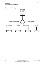
Page 62: ...rs Chancing colors lines or areas BacklightOK Illumination is not working partially working or not even Touchscreen is not working Goto Blank Display Troubleshooting Goto Faulty Display Troubleshooting Goto Touchscreen Troubleshooting Display electrical problems connection problems Display optical problems Pixel defects Goto Backlight Troubleshooting Display is dimm key leds not ok Display module ...

Page 63: ...ry with another display module Display working Yes No 12 5MHz clock detected Measure V28 from L4427 Voltage OK Measure display clock from C4444 No clock No End Yes Go to Power troubleshooting No Check C4439 C4440 L4427 components OK No Yes Replace broken components Display working No Yes Go to blank display troubleshooting page 2 Use oscilloscope and tap touchscreen before measuring clock is not a...

Page 64: ...pins 15 and 30 w ith oscilloscope No Replace Z4422 and Z4423 EMI filter Display working Yes No toggling No End Continues from blank display troubleshooting page1 Yes Start phone with display flex disconnected Reflash phone Display working No Yes Start phone again with display flex connected and retest Pins are display data lines There should be data toggling if phone is working ok Toggling Change ...

Page 65: ...touchscreen calibration and recalibrate if not ok Yes Check touchscreen connector X4421 filtering components R4440 L4420 L4423 L4425 C4402 C4409 R4460 R4463 No Check controller ChipSelect from R4400 Press touchscreen when measuring this Toggling Reflash phone No activity Touchscreen working Calibrate touchscreen Yes Change N4400 Working No Yes No Reflash phone Touchscreen working Yes No Phone alre...

Page 66: ...ct criteria specifies No action Check touchscreen calibration and re calibrate if needed End No No Is backlight brightness ok No See own chapter about pixel defects Is backlight power ok voltage from C4443 11 5 12 5V Go Backlight troubleshooting Use full brightness setting to check backlight problems Change display module calibrate touchscreen End No Display background color is clearly too yellowi...

Page 67: ...xel can be an individual red green or blue pixel Figure 1 RM 12 dots and pixels Pixel defect criteria Bright dots 3 or less or Black dots 3 or less Total max 3 No line defects Number of Dots Active Area Dot Pitch Pixel Per Inch Color Arrangement 640 RGB 320 40 32 80 64 mm 0 042 0 126 mm 201 59 RGB Stripe 640 dots B R G B R G B R B R G R G B B R G G G B G R B R Horizontal Direction 320 RGB dots FPC...

Page 68: ...RM 12 CCS Technical Documentation 66 COMPANY CONFIDENTIAL Issue 1 11 2004 Copyright 2004 Nokia All Rights Reserved Figure 2 Definition of 1 dot defect 1 or 2 defected horizontal sub pixels bright black ...

Page 69: ...RM 12 Nokia Customer Care Issue 1 11 2004 COMPANY CONFIDENTIAL 67 Copyright 2004 Nokia All Rights Reserved Backlight troubleshooting 1 ...

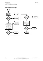
Page 70: ...ponents before point where VBAT voltage is lost Start from battery side VBAT Check also C4423 and R4446 value 27R soldering Check X4421 pin soldering C4425 VBAT No PWB failure Disable backlight from Control Panel Enable backlight from Control Panel Full brightness Yes D4420 pin 8 2 78V Use partial mode or adjust brightness period to lowest value to disable display backlight Verify functionality wi...

Page 71: ...current mirror components V4421 R4436 N4421 R4443 and backlight power components R4441 R4442 R4446 V28 should be found from C4438 Check connector X4421 soldering If upper backlight leds are not working are dimm but lower are bright problem in current mirror circuitry Backlight OK Yes END No R4446 0 50 0 51V R4442 1 50 1 51V No Goto backlight power troubleshooting page 2 Yes R4441 should have also ...

Page 72: ...tor and hall sensor soldering Resolder if needed Battery cover pull up resistor R4449 Check pull up resistor connection to V28 2 78V 0V Goto Power Troubleshooting Check battery cover that magnet is present Replace Hall sensor Check again hall sensor output from pin 3 0V Check hall sensor output from pin 3 with magnet 2 78V End 0V 0V Goto OMAP Troubleshooting Input line shortcircuited PWB or OMAP f...

Page 73: ...oose or missing Is keypad flex broken or connector disconnected from flex Replace button Yes Problem type Change A frame assembly Yes Check engine connector that is is properly assembled OK Change connector Yes Check components Z4420 R4451 R4452 OK Replace No End No No Yes No Problem in Baseband Goto BB troubleshooting End ...

Page 74: ...r by using a second known to be good device as a reference Experience significantly helps in analyzing image quality Terms Dynamic range camera s ability to capture details in dark and bright areas of the scene si multaneously See Image which has been taken against light The actual object is dark for ex ample Exposure time camera modules use silicon sensor to collect light and for forming an image...

Page 75: ...n practice the operation is such that close objects may be noticed to get more blurred when distance to them is shortened from 40 cm Lack of sharpness will be first visible in full reso lution 1152 x 864 images If observing just the viewfinder even very close objects may seem to appear sharp This is normal behavior do not change the camera module Figure 1 Image blurred due to too close distance to...

Page 76: ...ce is used in a moving car object skewing or tilting will occur This phenomenon is fundamental to most CMOS camera types and normal and can t be avoided Movement of camera or object will usually cause blurring in inside or dim light ing conditions due to long exposure time This is normal behavior do not change the camera module Figure 3 Near objects in image get skewed when shooting from a moving ...

Page 77: ... taken in 70 degrees Celsius 5 Phone display if the display contrast is set too dark the image quality degrades quite much the images may be very dark naturally depending on the setting If display contrast is set too bright image contrast appears bad and faint This flaw is easily cured by setting the display contrast to correct value This is normal behavior do not change the camera module 6 Basic ...

Page 78: ...d image This phenomenon may also result if pic tures are taken indoors under mismatch of 50 60 Hz electricity network fre quency The used electricity frequency will be detected automatically by the camera module In some very few countries both 50 and 60 Hz networks are present and thus probability for the phenomenon grows Flickering occurs also under high artificial illumination level This is norm...

Page 79: ...y visible lens glare phenomenon and poor contrast in images This happens due to unwanted reflections inside camera optics Generally this kind of reflections are common in all optical systems This is normal behavior do not change the camera module Figure 7 A lens reflection effect caused by sun shining above the scene Figure 8 A good picture taken indoor ...

Page 80: ...Nokia Customer Care RM 12 Issue 1 11 2004 Copyright Nokia All rights reserved Page 78 Figure 9 A good picture taken outdoors ...

Page 81: ...ction In this chapter some information of the actual construction of the camera module is given for getting understanding of the actual mechanical structure of the module Figure 10 Cross section of the camera module and assembly principle Figure 11 Bottom view including camera module serial numbering ...

Page 82: ...d for versioning Passive components Camera protection window is part of phone cover mechanics Dust gasket between lens unit and camera protection window Image quality analysis Possible faults in image quality When checking for possible errors in camera functionality knowing what error is suspected will significantly help the testing by narrowing down the amount of test cases The following types of...

Page 83: ...ses the phone If dust particle is lying on infrared filter surface on either side they are much harder to locate because they will be out of focus and appear in image as large grayish and fading edge blobs Sometimes they will be very hard to find and thus the user probably will not notice them at all since they do no harm But it is possible that a larger particle disturbs the user causing need for...

Page 84: ... found a couple of test images should be taken and checked Generally a well illuminated typical indoor office scene such as the one in Figure A good picture taken indoor can be used as a target The main considerations are The protection window has to be clean Amount of light 300 600 lux bright office lighting is sufficient The scene should contain e g small objects for checking sharpness and dista...

Page 85: ... of images demonstrates the effects of fingerprints on the camera protec tion window It should be noted that the effects of any dirt in images can vary very much it may be difficult to judge if the window has been dirty when some image has been taken or if something else has been wrong That is why the cleanness of the protection window should always be checked and the window should be wiped clean ...

Page 86: ...target when analyzing this kind of errors The errors will be clearly visible as colorful sharp dots or lines in camera images See Example about bit errors caused by JPEG compression One type of bit error is lack of bit depth In that case image is almost totally black under normal conditions sensing something only under very high illumination Typically this is a contact problem between the camera m...

Page 87: ...RM 12 Nokia Customer Care Page 85 Copyright Nokia All rights reserved Issue 1 11 2004 Figure 15 Example about bit errors caused by JPEG compression ...

Page 88: ...roperly Is it working now Is Camera module properly fixed Change Camera Re run the test Is it pass Yes Yes No No Is the Camera working now End Go to Camera baseband HW troubleshooting Yes No Check X4420 solder joints and flex connection Is it OK Run ST_CAMERA_IF self test in Phoenix Is the result pass No Yes No Change 4434 Re run the test Is it pass Yes No Yes No No Yes Yes Change N ...

Page 89: ... 2 6V Measure voltage from pin 3 of D4405 Is it 2 7V to 2 9V Measure ExtClk waveform at D4405 pin 6 against ground Is frequency 9 6MHz and amplitude 1 7V to 2 6V Measure ExtClk waveform at D4405 pin 1 against ground Is frequency 9 6MHz and amplitude 2 7 to 2 9V Measure I2C waveform at connector X4420 10 and 11 Both signals operating and amplitude 1 8V nominal Check I2C waveforms and operation at R...

Page 90: ...Nokia Customer Care RM 12 Issue 1 11 2004 Copyright Nokia All rights reserved Page 88 Bad image quality ...

Page 91: ...RM 12 Nokia Customer Care Page 89 Copyright Nokia All rights reserved Issue 1 11 2004 FM Radio troubleshooting FM radio component layout Trace Layout ...

Page 92: ...3 R6102 and R6100 and measure 32kHz clock signal from J6103 and retest starting Does it start now Does the radio start OK retest Baseband digital failure UPP Connect RF test signal note 1 Set radio channel to 98 0 MHz Set radio volume to maximum Measure audio signal from J6128 and J6129 Is it 1 kHz 0 5 0 8 Vp p Check C2032 C2033 C2037 C2039 L2026 C6104 C6109 C6115 L6102 Measure signal from J6128 a...

Page 93: ...n Df 75 kHz Modulating frequency fm 1 000 kHz RF generator internal FM stereo mode R L pilot state ON Pictures of FM radio signals Figure 16 Audio output from FM radio test points J6128 and J6129 or J2023 and J2024 with FM test signal Figure 17 FM radio clock from test point J6103 32 kHz frequency clock signal when radio is on ...

Page 94: ...al RES BW 10 kHz VBW 10 kHz SWP 1 00 sec AT 0 dB REF 20 0 dBm LOG 10 dB CENTER 98 0000 MHz SPAN 300 0 kHz 71 03 dBm MKR 97 9280 MHz PEAK WA SB SC FS CORR 15 51 49 03 JUL 2002 SWEEP CONT SGL FREE RUN VIDEO LINE EXTERNAL SYNC CRD TV TRIG RES BW 10 kHz VBW 10 kHz SWP 20 0 msec AT 10 dB REF 0 dBm LOG 10 dB CENTER 196 450 MHz SPAN 1 000 MHz 9 40 dB MKR 196 440 MHz MEAS UNCAL PEAK WA SB SC FS CORR 10 46...

Page 95: ...USB device No Yes Start with phone with battery Connect the phone to PC via USB with known good DKU2 cable PC recognizes the phone as USB device No Goto USB troubleshooting page 2 Connect a service battery to phone Check that the startup mode selection is NORMAL Connect to PC with service battery USB plug inspect also production test pattern where the service battery connects for damage litter PC ...

Page 96: ...d resistor R2004 Check APE GPIO3 from R2004 2 8V No Yes PC recognizes the phone as USB device Yes No Replace EMI filter R2003 PC recognizes the phone as USB device Go to OMAP1510 troubleshooting No End Change L2002 PC recognizes the phone as USB device Yes No End Go to OMAP1510 troubleshooting Yes End Continued from USB troubleshooting page 1 Measure resistance to GND from D pin 6 and D pin 7 on X...

Page 97: ...es the BC3 Bluetooth solution troubleshooting for CCS AMS Bluetooth Settings for Phoenix General setup Connect phone to Phoenix in local mode select product from the prod uct menu Choose Testing Bluetooth locals Run BER test when JBT 9 box in close to BT antenna in 10 centime ters Figure 20 An example of Phoenix settings for Bluetooth troubleshooting ...

Page 98: ...heck Vreg in 2 8V from C6036 capasitor Is it OK Check VDD_ANA 1 8V from capasitor C6031 Change BC3 Repeat BER test Repeat BER Test OK BER 0 1 NOK OK NOK NOK NOK OK OK NOK NOK NOK Repeat BER Test OK Check BC3 Xtal_in freq 12MHZ swing 400 900mV R6043 ok Check regulator 2 8V from C4202 and N4200 from APE power checking sheet Check RF path components L6031 L6032 C6046 soldering resolder Check BT clock...

Page 99: ...RM 12 Nokia Customer Care Page 97 Copyright Nokia All rights reserved Issue 1 11 2004 Figure 22 Bluetooth problems 1 Figure 23 Bluetooth problems 2 ...

Page 100: ...Nokia Customer Care RM 12 Issue 1 11 2004 Copyright Nokia All rights reserved Page 98 Figure 24 Bluetooth assembly drawing ...

Page 101: ... End Yes No InitializeMMC check GPIO15 voltage from R5202 2 8V Goto OMAP1510 troubleshooting Yes No ChangeMMC regulator N5200 and capacitors C5201 C5203 MMC initializationis done at first access after 10sec of idle time voltage drops to zero Use oscilloscope Go to MMC troubleshooting page 2 Start Frequency 16MHz during data transmission 400kHz during initialization All measurements provide that th...

Page 102: ... MMC working Replace R5200 Connector damaged Replace connector X5200 Yes Signals correct at connector X5200 No Yes End Yes Signals correct at X5200 Yes MMC working Yes No No No No Go to OMAP1510 troubleshooting End From MMC troubleshooting page 1 No Connector X5200 soldering damaged Yes End MMC working Yes No ...

Page 103: ...connector X2021 Change user s headset END YES NO NO Does headset earpiece working Does headset microphone work during a call Does remote control switch work YES Follow the trouble shooting flow chart for External earpiece faults NO Follow the trouble shooting flow chart for External MIC faults NO YES YES NO Measure HOOKINT at R2121 UEM side Is it low 1 1V when headset button is pressed Check compo...

Page 104: ...toring of the BSI signal is done by a comparator inside UEM The threshold voltage is calculated from the battery size specifications The SIM interface is powered up when the SIMCardDet signal indicates card in This signal is derived from the BSI signal SW tries first to power up the SIM with 1 8 V If this does not succeed power up is repeated with VSIM switched to 3 V The data communication betwee...

Page 105: ...okia All rights reserved Issue 1 11 2004 Figure 26 SIM Power Up Figure 27 SIM answer to reset Ch1 Vsim Ch2 Reset Ch3 Clock Ch4 I O Measured with 3Vsim SIM answer to reset CH1 SIM_CLK CH2 SIM_RST CH3 SIM_I O CH4 SIM_PWR Measure points SIM connector ...

Page 106: ... RM 12 Issue 1 11 2004 Copyright Nokia All rights reserved Page 104 Figure 28 SIM Clk 3 25MHz NOTE Remember to check the two PHOENIX test cases before changing UPP SIM_Clk_3 25MHz CH1 SIM_CLK Measure points SIM connector ...

Page 107: ... connector Is it OK Check clean battery centre contact Verify BSI signal has a steady voltage Measure VSIM Is it 1 8 3 0V when SIM interface is powered up Measure VSIM resistance to GND Is it low Check C471 Is it OK Change VSIM decouple C471 Change SIM ASIP R496 Check Clk RST DATA at SIM connector Are the signals Check Clk RST DATA between UEM and the SIM ASIP Change SIM ASIP R496 present Are the ...

Page 108: ...nics when the rotating mass has contact to it Vibra Malfunction Vibra is continuously on Vibra is noisy Vibra doesn t rotate Check the surrounding mechanics of the Vibra Is the Vibra jammed or its contact pads worn Is it Vibra component itself that makes noise Measure that C134 is pulsed down to zero while Vibra is switched on Check C134 C135 V132 and V131 Change UEM Vibra works Change the Vibra a...

Page 109: ... Camera RF ASIC Helgo VCXO Crystal SDRAM ZOCUS CMT FlashClk max 54MHz APE SYSClk 12MHz SIM MMC 1 8 2 8 V level shifter Audio DAC BCLK 12MHz I2C SCK 400 kHz SDRAMClk 75MHz I2S Clk 6MHz PCMCLK 267kHz CamClk 12MHz XABUS 12MHz SleepClk 32kHz CBUSClk 1MHz DBUSClk 13MHz SIMClk 3 25MHz Display DOTClk 12 5MHz RFClk 26MHz SleepClk 32kHz 2 8V SCU Clk 13MHz Camera converter ...

Reviews: