background image

18

WAAS GUS Signal Generator User Guide Rev 1

Chapter 2

Minimum Connections

15. Monitor your L1 and L5 data using available logs and commands from the Receiver through the Test PC.

The sections of 

Chapter 3, Setup Considerations on Page 19

 give further details on steps #1 to #13 whil

Chapter 

4, Operation on Page 24

 helps with step #14. See the Signal Generator specific command and logs in 

Chapter 5, 

Messages on Page 26

For other commands and logs available with the Receiver, please refer to its WAAS G-III 

Reference Receiver user manual (

OM-20000137).

Summary of Contents for 01020347

Page 1: ...OM 20000187 v1 November 2019 WAAS GUS Signal Generator USER GUIDE ...

Page 2: ...to prohibition against further use and disclosure The information provided herein may be disclosed by the Customer for any purpose related to the use and operation of related NovAtel supplied equipment including without limitation maintenance revision of equipment design upgrades testing and any other required Customer activity This Notice must be marked on any reproduction of these data in whole ...

Page 3: ...3 2 4 CMP and WMP 21 3 2 5 Code PPS Output 21 3 2 6 1PPS In 21 3 2 7 10 MHz In and 10 MHz Out 21 3 2 8 RF Out 22 3 2 9 IF Out 22 4 Operation 24 4 1 Communications with the Signal Generator 24 4 1 1 Serial Port Default Settings 24 4 1 2 Communicating Using a Remote Terminal 24 4 1 3 Communicating Using a Personal Computer 24 4 2 Message Control and Data Lines 24 4 2 1 Other Control Lines 25 5 Messa...

Page 4: ...AS GUS Signal Generator User Guide Rev 1 Table of Contents 6 3 Decompressing the Files 47 6 4 Running WinLoad 47 6 4 1 Open a File to Download 48 6 4 2 Downloading firmware 50 A Technical Specifications 51 ...

Page 5: ...ch 17 7 Signal Generator Front Panel 19 8 Close up of Connectors on Rear Panel 20 9 RS 485 Symbol Timing Diagram 25 10 Application of Frequency Chipping Rate Ramp 35 11 Input Command Flowchart 36 12 Serial Number and Version Label 46 13 Main Screen of WinLoad 48 14 WinLoad s Open Dialog 48 15 Open File in WinLoad 49 16 COM Port Setup 49 17 Update Process Complete 50 18 Signal Generator Dimensions ...

Page 6: ...ce Field 32 23 L1 I Channel G2 Coder Initialization Field 32 24 L1 Q Channel G2 Coder Initialization Field 33 25 L5 I Channel XB I Coder Initialization Field 33 26 L5 Q Channel XB Q Coder Initialization Field 33 27 L1 L5 Code Chip Rate and Carrier Frequency Command Fields 34 28 Code Chip Rate Field 34 29 Code Chip Rate Ramp Field 34 30 Carrier Frequency Field Bit Format 34 31 Carrier Frequency Ram...

Page 7: ...7 49 CRC 16 CCITT Checksum Field 44 50 CRC 16 CCITT Checksum Field 44 51 CRC 16 CCITT Characteristics 44 52 Errors 45 53 Target Card Identification 49 54 L1 and L5 WMP Connector Pin Out Descriptions 54 55 L1 and L5 CMP Connector Pin Out Descriptions 54 ...

Page 8: ...Case History login access required Web Portal https novatelsupport force com community login E mail support novatel com Telephone U S and Canada 1 800 NOVATEL 1 800 668 2835 International 1 403 295 4900 WAAS GUS Signal Generator Firmware Updates Firmware updates are firmware revisions to an existing model which improves basic functionality of the signal generator The process for obtaining firmware...

Page 9: ...ation of FCC and CE Marking rules and void the user s authority to operate this equipment Where applicable follow the electrical codes for the country of installation Examples of country codes include USA National Electrical Code NFPA 70 Canada Canadian Electrical Code CSA C22 UK British Standards Institute BSI 7671 To maintain compliance with the limits of a Class A digital device you must use pr...

Page 10: ...related inquiries The WAAS GUS Signal Generator utilizes a comprehensive user interface command structure which requires communications through its WAAS Message Processor WMP communications COM ports WAAS GUS Signal Generator commands and logs can be found in Chapter 5 Messages starting on Page 26 What s New in Rev 1 of this manual Describes the WAAS GUS Signal Generator Quadrature channel enhance...

Page 11: ...ected 1023 bit PRN code In phase I channel I channel with dataless quadrature Q channel or I channel with independent data on the Q channel User configurable 1227 6 MHz default or 1575 42 MHz alternate RF output signal carrying the configured modulation for L1 L5 codes with PRN values of 120 to 158 inclusive selectable using the Initialization Command see Page 30 70 MHz BPSK or QPSK modulated IF o...

Page 12: ...l Generator 14 RF Switch 5 Receiver WAAS G III 15 L Band Filter and Low Noise Amplifier 6 RS 485 message input from CMP 16 L1 and L5 at L2 SIGGEN RF loop 7 RS 232 command input from WMP 17 L1 and L5 TLT 8 GPS antenna 18 L1 and L5 GEO or TLT 9 Test loop translator 19 Power combiner splitter 10 C1 C5 uplink Figure 1 shows a high level implementation of a WAAS GUS setup see Chapter 2 Minimum Connecti...

Page 13: ...ator The L5 IF output has the L5 signal structure with an IF bandwidth of 22 MHz The Signal Generator provides two loopback signals that are monitored by the WAAS G III Receiver These RF signals are frequency upconverted replicas of the 70 MHz L1 and L5 outputs By default the 70 MHz L1 is upconverted to 1227 6 MHz Similarly by default the 70 MHz L5 is upconverted to 1176 45 MHz The user can select...

Page 14: ... Q channel See also Section 5 1 3 2 Control Command starting on Page 28 Figure 3 shows the interfaces of the Signal Generator Figure 3 Interface Block Diagram After a cold start or after a power reset the Signal Generator performs an Initiated Built in Test IBIT memory self test and internal calibration Provided a 1PPS reference source is made available to the Signal Generator it can receive WAAS ...

Page 15: ...S Reference Source L1 and or L5 IF Output to the Satellite Uplink path as the main Signal Generator output signal L1 and or L5 RF Output to the local Signal Generator signal monitoring facility All of the above connections are described in more detail in Chapter 3 Setup Considerations To demonstrate and or experiment with signals generated by the Signal Generator in a test environment outside of t...

Page 16: ...m 3 1 RF Combiner SMA 9 50 dB SMA Coaxial Attenuators 50 ohm 10 SMA Coaxial DC block the WAAS G III Receiver RF1 In outputs DC power by default 11 DB 9 Serial Cable 12 USB Cable Type A to micro USB NovAtel P N 60723119 13 50 ohm Coaxial Cable Male TNC to Male SMA NovAtel P N 60423064 14 50 ohm Coaxial Cable Male Type N TNC to Male SMA 15 120 VAC Power Cable NovAtel P N 60723070 16 50 ohm Coaxial C...

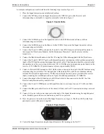
Page 17: ... so that the signal power at the receiver input is between 105 to 90 dBm given an input noise power density to the receiver of 150 dBm Hz Typical attenuator vales are approximately 50dB 8 Connect a Powered GPS Antenna to a LNA which is then connected to the input of the RF Combiner using interconnecting coaxial cables The total gain due to the antenna LNA cable losses combiner and any external LNA...

Page 18: ...Test PC The sections of Chapter 3 Setup Considerations on Page 19 give further details on steps 1 to 13 while Chapter 4 Operation on Page 24 helps with step 14 See the Signal Generator specific command and logs in Chapter 5 Messages on Page 26 For other commands and logs available with the Receiver please refer to its WAAS G III Reference Receiver user manual OM 20000137 ...

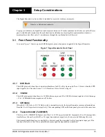
Page 19: ...ut signal is lost See also Section 5 1 4 6 Hardware Status Fields on Page 41 3 1 2 10 MHz This LED glows green when there is a 10 MHz reference present The 10 MHz reference input level is in the range 12 to 14 dBm and has an impedance of 50 ohms 3 1 3 CW Mode When the L1 CW Only or L5 CW Only switch is manually selected the Signal Generator removes all modulation from the L1 or L5 signal carrier r...

Page 20: ...erator require careful insertion and removal Observe the following when handling the cables To insert a cable make certain you are using the appropriate cable for the port the serial cable has a different connector DB9 than the PPS cable TNC or the RF cable N Type connectors 3 2 1 Power After initial connection of the power supply to the Signal Generator and pressing the power switch on the back o...

Page 21: ...nd L5 Code PPS Out ports allow synchronization of external test equipment with the modulated L1 or L5 signal available respectively 3 2 6 1PPS In The 1PPS level is an active low pulse with TTL levels driving an input impedance of 3 k It is also factory configurable to use active high pulses and or a 50 AC coupled input impedance The pulse width of the 1PPS update is 200 microseconds nominally with...

Page 22: ...ip rate The L5 RF output modulation chip rate is 10 23 MHz The RF output modulator phase on accuracy is within 3 degrees For further information on the signals or connector type for the RF Out connectors please see Input Output Connectors on Page 52 3 2 9 IF Out The L1 and L5 IF Out connectors provide a 70 MHz Intermediate Frequency IF signals from the Signal Generator It is normally used to provi...

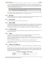
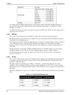
Page 23: ...ng conditions identified in Section 5 2 Error Handling on Page 44 The L5 signal is filtered with a 22 MHz IF filter having the characteristics described in Table 4 Table 4 L5 IF Bandwidth Requirements The L5 CW Only switch forces the unit to remove all modulation from the signal carrier I and Q signals both forced to zero The output impedance for the L1 and L5 IF Output is 50 Ohms Offset from Carr...

Page 24: ...s proper RS232 interface with your data terminal To communicate with the terminal the Signal Generator requires the RX TX RTS CTS and GND lines to be used Ensure that the terminal s communications set up matches the Signal Generator s RS232 protocol 4 1 3 Communicating Using a Personal Computer A PC can be set up to emulate a remote terminal as well as provide the added flexibility of creating mul...

Page 25: ... transmitted and the output of both the I and Q shall be inhibited If only in phase I data is enabled and a second set of 500 bits is provided the second set of 500 bits shall be discarded however the first set of 500 bits shall be transmitted normally as the I data After MSGRDY has been asserted the Signal Generator sends its first clock within 1 microsecond of the assertion After the 500th clock...

Page 26: ...transmitted to the WMP also have these synchronization bytes encoded to the hex value 0xAA5555AA Table 6 shows the Packet Synchronization field Table 7 shows the Packet Synchronization field byte and bit order Table 6 Packet Synchronization Field Table 7 Packet Synchronization Field Bit Format 5 1 2 L1 L5 Indication Field This field consists of one 1 byte containing the L1 or L5 indication flag If...

Page 27: ...ntifier byte field and bit order Table 12 on Page 28 shows the Command Message Identifier bit fields Field Bytes Byte Position L1 L5 Destination WMP Destination 2 1 Byte 4 4 L1 1 L5 5 1 L1 L5 5 Byte 4 D7 D6 D5 D4 D3 D2 D1 D0 MSB LSB Field Bytes Byte Position Description 3 1 1 Byte 5 5 Command Message Identifier Field 3 2 1 Byte 6 6 Control Command Data Field 3 3 1 Byte 7 7 Symbol Rate Field 3 4 1 ...

Page 28: ...the I and Q coders have been reset initialized and advanced to the correct state Table 13 L1 L5 Control Command Bit Fields Byte 5 D7 D6 D5 D4 D3 D2 D1 D0 MSB LSB Bit Command message WMP to Signal Generator Command Message ID Field D0 Control Command 0x01 D1 Initialization Command 0x02 D2 Code Chip Rate and Carrier Frequency Command 0x04 D3 Reserved for future use 0x08 D4 Reset Command 0x10 D5 Rese...

Page 29: ... FIELD If this field flag is set the Signal Generator disables the NH code for dataless operation or for the L5 I channel signal only the Manchester Code for data operation Note that Manchester coding is not used on the L1 I channel signal DISABLE MESSAGE Q FIELD If this field flag is set the Signal Generator does not use the Q message symbols in modulation DISABLE PRN CODE Q FIELD If this field f...

Page 30: ...le Enable Disable Enable 1 0 0 1 Enable Disable Enable Disable 1 0 1 0 Enable Disable Disable Enable 1 0 1 1 Enable Disable Disable Disable 1 1 0 0 Disable Enable Disable Enable 1 1 0 1 Disable Disable Enable Disable 1 1 1 0 Disable Disable Disable Enable 1 1 1 1 Disable Disable Disable Disable 0 N A N A N A N A N A N A N A D3 D1 D5 D2 PRN Code Manchester Code Neumann Hoffman Code Symbols Byte Pos...

Page 31: ...s 0 7 Byte 16 init bits 8 9 G2 Q channel coder initialization value at zero chip Count Set to zero if not used Byte Position Description Valid Range Value Scale Factor Byte 7 Symbol Rate RF Configuration 0 or 128 Set to zero 0 Byte 8 Sub Chip 0 255 Initial Sub Chip Load Byte 9 10 Code Chip Advance 0 10229 Initial Code Chip Advance Byte 11 12 Symbol Advance and Symbol 1 ms epoch Bits 0 14 0 499 Bit...

Page 32: ...eld bit format If 500 SPS is selected the MSB indicates which 1 ms epoch is selected within the initial symbol epoch A 0 indicates that the even 1 ms epoch is selected within the initial 2 ms symbol epoch A 1 indicates that the odd 1 ms epoch is selected within the 2 ms symbol epoch Table 22 Symbol Advance Field L1 I CHANNEL G2 CODER INITIALIZATION FIELD This field contains the initial state 10 bi...

Page 33: ...rms the new Code Chip Rate and Carrier Frequency for either L1 or L5 to be assigned at the next 1PPS update pulse and the Code Chip Rate Ramp and Carrier Frequency Ramp to be assigned at the update periods following the next 1PPS update pulse The Code Chip Ramp Rate or Carrier Frequency Ramp can be set to zero if no ramp update is to be performed every update period 250 ms If the Code Chip Ramp Ra...

Page 34: ...o be assigned at the next 1PPS update pulse See Table 30 for the Carrier Frequency field byte and bit order format Table 30 Carrier Frequency Field Bit Format Byte Position Description Valid Range Scale Factor Data Byte 17 22 Code Chip Rate 1 023 0 25 1540 Mcps L1 10 23 0 25 115 Mcps L5 LSB 75 x 2 48 Mcps Data Byte 23 24 Code Chip Rate Ramp 8 525 10 6 cps 250 ms L1 8 525 10 5 cps 250 ms L5 LSB 75 ...

Page 35: ... operational When this command is received the Signal Generator performs the actions as shown in Figure 11 on Page 36 There are no data fields associated with this command 5 1 3 6 Watchdog Timer The watchdog performs a Signal Generator board reset if it is not serviced for 3 seconds due to a software failure The software services the watchdog as frequently as possible to prevent the watchdog from ...

Page 36: ...36 WAAS GUS Signal Generator User Guide Rev 1 Chapter 5 Messages Figure 11 Input Command Flowchart ...

Page 37: ... the sub phase of the code chip latched within the current 1 ms epoch upon detection of a 1PPS update pulse Table 34 on Page 38 shows the Uplink Range Code Chip Sub Phase field byte and bit order Field Bytes Byte Position Description 3 1 2 Byte 5 6 Uplink Range Code Chip Sub Phase 3 2 2 Byte 7 8 Uplink Range Code Chip Counter 3 3 2 Byte 9 10 Uplink Range Symbol Counter 3 4 1 Byte 11 11 Switch Stat...

Page 38: ... initial symbol epoch A 0 indicates that the even 1 ms epoch is latched within the initial 2 ms symbol epoch A 1 indicates that the odd 1 ms epoch is latched within the 2 ms symbol epoch Table 36 Uplink Range Symbol Counter Field 5 1 4 4 Switch Status Fields The Switch Status field contains the current state of all Signal Generator switches The switch settings are polled when the Status Message is...

Page 39: ...y Switch is open and that the Signal Generator is not in CW mode 5 1 4 5 Error Status Fields The Error Status field contains any errors that may have occurred during the last 1 second epoch The Error Status field bits are reset to zero after the status message is sent Table 39 shows the Error Status field byte and bit order Table 40 on Page 39 shows the Error Status bit fields Table 39 Error Statu...

Page 40: ... ON RECEIVED DATA FIELD If a 1 this flag indicates that the UART detected an overrun error in one or more command bytes during the previous 1 second epoch This flag is reset after the status message has been transmitted RECEIVE DATA SYNC ERROR FIELD If a 1 this flag indicates that the Signal Generator did not receive a valid sync byte in a command packet during the previous 1 second epoch This fla...

Page 41: ...ld bit order Table 42 shows the Hardware Status bit fields Table 41 Hardware Status Field Table 42 Hardware Status Bit Fields 10 MHZ PRESENT FIELD This flag indicates if the 10 MHz clock signal is present If a 1 then the 10 MHz signal is present If a 0 then the 10 MHz signal is absent CLOCK CIRCUIT FAULT FIELD This flag indicates if the clock circuit board is faulty If a 1 then the clock circuit b...

Page 42: ...ommand is received and all internal calibrations have been performed REFERENCE 1PPS PRESENT FIELD The flag indicates if the 1PPS reference is present If this bit is set to 1 the 1PPS signal is present If this bit is set to 0 the 1PPS signal is not present 5 1 4 7 Reset Command Second Epoch Counter This field contains the number of one second epochs counted since the last hardware reset occurred or...

Page 43: ...order and format for this field Table 46 FPGA Version Number Field 5 1 4 11 Signal Generator State This field contains the state of the Signal Generator during the previous one second epoch Table 47 shows the byte order and format for this field Table 48 on Page 43 shows the Signal Generator state values Table 47 Signal Generator State Field Table 48 Signal Generator State Value LS Byte 24 MS Byte...

Page 44: ...field and Table 50 on Page 44 shows its bit format The characteristics for the CRC 16 CCITT are shown in Table 51 on Page 44 Table 49 CRC 16 CCITT Checksum Field Table 50 CRC 16 CCITT Checksum Field Table 51 CRC 16 CCITT Characteristics 5 2 Error Handling Table 52 shows the Signal Generator error conditions and their corresponding handling methods Field Bytes Byte Position Description Range 4 2 By...

Page 45: ...message truncated I and Q set to zero and Transmitter disabled Report status CMP MSGRDY stuck high I and Q set to zero and Transmitter disabled Report status CMP MSGRDY stuck low I and Q set to zero and Transmitter disabled Report status MSGDATA not ready when needed I and Q set to zero and Transmitter disabled Report status ...

Page 46: ...ignal Generator is to contact the NovAtel Customer Support using the contact information on Page 8 When you call be sure to have the WAAS GUS Signal Generator s serial number and program revision level available This information is printed on the rear panel of the Signal Generator as shown in Figure 12 Figure 12 Serial Number and Version Label You can also verify the information First power up the...

Page 47: ... an appropriate directory on your computer each file must be decompressed A Windows based dialog is provided for password entry The self extracting archive then generates the following files WinLoad exe WinLoad utility program HowTo txt Instructions on how to use the WinLoad utility WhatsNew txt Information on the changes made in the firmware since the last revision Application Firmware File Name ...

Page 48: ...me you will need to make sure the file and communications settings are correct 6 4 1 Open a File to Download From the file menu choose Open Use the Open dialog to browse for your file see Figure 14 Figure 14 WinLoad s Open Dialog Once you have selected your file the name should appear in the main display area and in the title bar see Figure 15 9600 ...

Page 49: ...dentification 6 4 1 1 Communications Settings To set the communications port and baud rate select COM Settings from the Settings menu see Figure 16 Choose the port on your PC from the Com Port drop down list and the baud rate from the Download Baudrate drop down list The Download Baudrate can be set to 9600 or 115200 while the Connect Baudrate should be set to 9600 Figure 16 COM Port Setup Entry D...

Page 50: ...d power cycle the Signal Generator turn it off and then on again 6 WinLoad should be able to locate the card and the hex file should start downloading 7 The Signal Generator should finish downloading and reset The process is complete when Done is displayed in the main display area see Figure 17 Figure 17 Update Process Complete 8 Close WinLoad This completes the procedure required to update a Sign...

Page 51: ...e Rev 1 51 Appendix A Technical Specifications A 1 Signal Generator Figure 18 Signal Generator Dimensions PHYSICAL Size 432 mm 17 0 x 406 mm 16 0 x 133 mm 5 2 Weight 9 8 kilograms 21 4 lb MECHANICAL DRAWINGS Dimensions are in millimeters ...

Page 52: ...ow there are 2 of these Ground Screw Length of Stud 3 8 Stud Thread 8 32 L1 WMP DE9P Connector L5 WMP DE9P Connector PPS Input Connector TNC female jack Signal Description A one pulse per second normally high active low pulse between 10 microsecond to 1 millisecond where the falling edge is the reference Level Voltage High 2 0 VDC Low 0 80VDC L1 or L5 1PPS Output Connector TNC female jack Signal D...

Page 53: ...nector Type N female jack Frequency Default 1176 45 MHz L5 Alternate 1227 6 MHz L2 Bandwidth 22 MHz Level 50 dBm 3 dB Impedance 50 VSWR 2 1 max at the center frequency 10 MHz Input Connector TNC female jack Sensitivity 13 1 dBm Impedance 50 10 MHz Output Connector TNC female jack RF Output Power 3 3 dBm Impedance 50 Phase Noise internal OCXO only 10 Hz 100 Hz 1 kHz 10 kHz 125 dBc Hz max 155 dBc Hz...

Page 54: ...55 L1 and L5 CMP Connector Pin Out Descriptions Pin No Direction Name 1 Reserved 2 Out TxD 3 In RxD 4 Reserved 5 GND 6 Reserved 7 In CTS 8 Out RTS 9 Reserved Pin No Direction Name 1 GND 2 Out MSGCLKa 3 In MSGRDYa 4 Reserved 5 In MSGRDATAa 6 In RESETa 7 GND 8 Reserved 9 In TXINHb 10 Reserved 11 12 13 In MSGDATAb 14 Out MSGCLKb 15 Reserved 16 In MSGRDYb 17 In TXINHa 18 Reserved 19 20 21 22 In RESETb...

Page 55: ...f the Signal Generator to an external power source 100 to 240 VAC An input voltage outside of this range may physically damage the unit voiding the warranty The power supply automatically adapts its input power to the national power source in the country of use as long as it is within the above range and you have an adapter for your local power receptacle Figure 19 Power Cable ...

Page 56: ...OM 20000187 Rev 1 November 2019 ...

Reviews: