ISD91200 Series Technical Reference Manual
Release Date: Sep 16, 2019
- 174 -
Revision 2.4
5.7.3
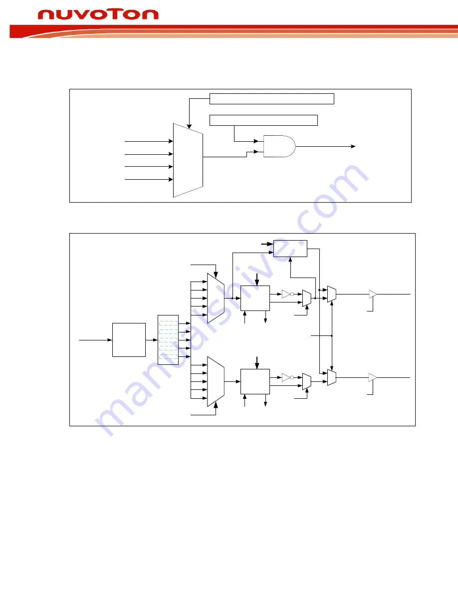
PWM Generator Architecture
The following figures illustrate the architecture of the PWM.
11
10
01
00
HCLK
CLK32K
CLK10K
CLK48M
PWM0CH01SEL
(CLK_CLKSEL1[29:28])
PWM0CH01EN(CLK_APBCLK0[20])
PWM0CH01_CLK
Figure 5-24 PWM Generator Clock Source Control
CSR1(CSR[6:4])
1
1/2
1/4
1/8
1/16
100
000
1
1/2
1/4
1/8
1/16
001
010
011
100
000
1
1/2
1/4
1/8
1/16
001
010
011
CSR0(CSR[2:0])
8-bit
Prescaler
PPR.CP01
PWM-
Timer0
Logic
PWM-
Timer1
Logic
1
0
1
0
Dead Zone
Generator 0
1
0
1
0
DZI01
DZEN01
CH0INV
CH1INV
PWMIE0 PWMIF0
PWMIE1 PWMIF1
Clock
Divider
CNR1, CMR1,
PCR
CNR0, CMR0,
PCR
PWM0CH01_CLK
(from clock
controller)
POE.PWM0
PA.12/PWM0
PA.13/PWM1
POE.PWM1
Figure 5-25 PWM Generator Architecture Diagram
5.7.4
PWM-Timer Operation
The PWM period and duty control are configured by the PWM down-counter register
(PWMx_PERIODx) and PWM comparator register (PWMx_CMPDATx). Formulas for calculating the
pulse width modulation are shown below and demonstrated in Figure 5-26 PWM Generation Timing.
Note that the corresponding GPIO pins must be configured as the alternate function before PWM
function is enabled.
PWM frequency = PWM0CH01_CLK/(p1)*(clock divider)/(1);
Duty cycle = (CMP+1)/(1).
CMP >= PERIOD: PWM output is always high.


