background image


ISD94100 Series Technical Reference Manual 


Sep 9, 2019 

Page 

125

 of 928 

Rev1.09 

IS

D

9

410

0

 S

ER
IE


T

E

C

HN

ICA
L

 RE

F

E

RE

NCE

 M

AN
U

AL


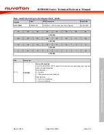
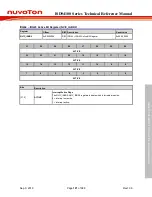
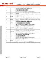
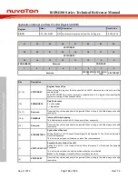
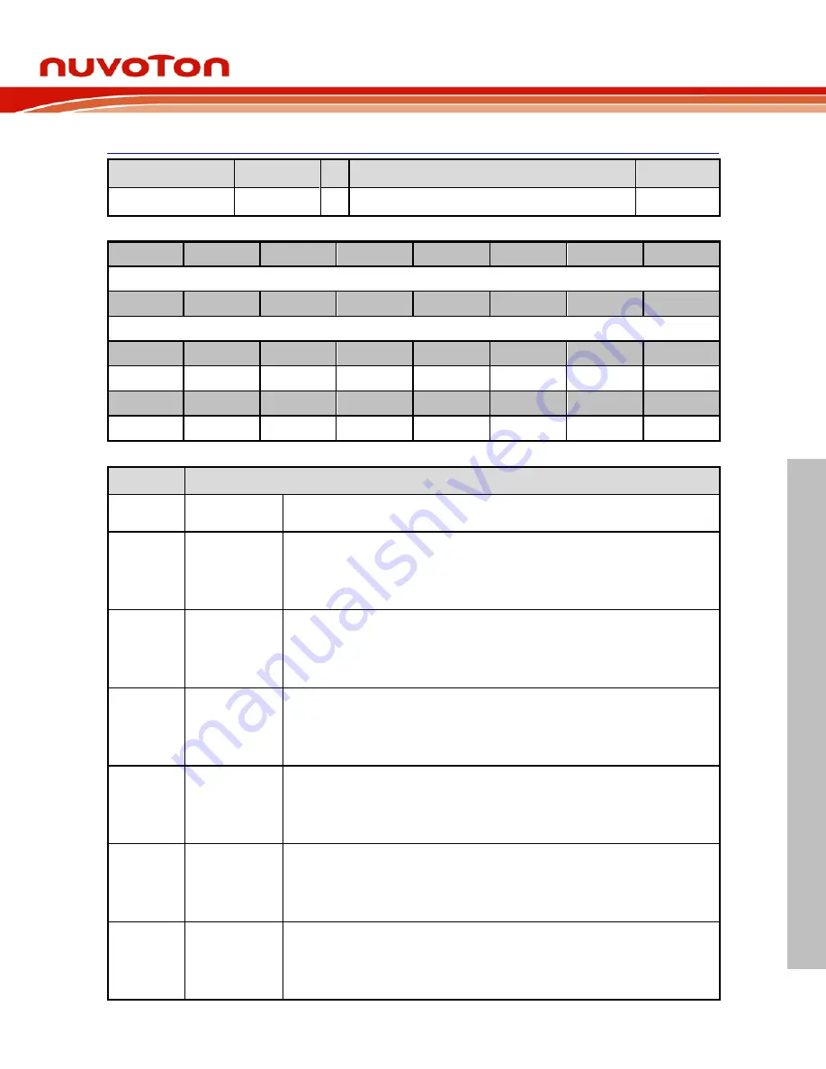
NMI Source Interrupt Enable Register (NMIEN) 


Register 

Offset 

R/W  Description 

Reset Value 

NMIEN 

0x00 

R/W  NMI Source Interrupt Enable Register 

0x0000_0000 


31 

30 

29 

28 

27 

26 

25 

24 

Reserved 

23 

22 

21 

20 

19 

18 

17 

16 

Reserved 

15 

14 

13 

12 

11 

10 

Reserved 

UART0_INT 

EINT5 

EINT4 

EINT3 

EINT2 

EINT1 

EINT0 

Reserved 

RTC_INT 

Reserved 

CLKFAIL 

SRAM_PERR  PWRWU_INT 

IRC_INT 

BODOUT 


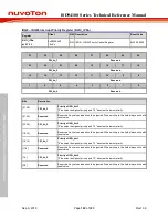
Bits 

Description 

[31:15] 

Reserved 

Reserved. Any values read should be ignored. When writing to this field always write with 
reset value. 

[14] 

UART0_INT 

UART0 NMI Source Enable (Write Protected) 

0 = UART0 NMI source Disabled. 

1 = UART0 NMI source Enabled. 

Note: 

This bit is write protected. Refer to the SYS_REGLCTL register. 

[13] 

EINT5 

External Interrupt 5 NMI Source Enable (Write Protect) 

0 = External interrupt 5 NMI source Disabled. 

1 = External interrupt 5 NMI source Enabled. 

Note: 

This bit is write protected. Refer to the SYS_REGLCTL register. 

[12] 

EINT4 

External Interrupt 4 NMI Source Enable (Write Protected) 

0 = External interrupt 4 NMI source Disabled. 

1 = External interrupt 4 NMI source Enabled. 

Note: 

This bit is write protected. Refer to the SYS_REGLCTL register. 

[11] 

EINT3 

External Interrupt 3 NMI Source Enable (Write Protected) 

0 = External interrupt 3 NMI source Disabled. 

1 = External interrupt 3 NMI source Enabled. 

Note: 

This bit is write protected. Refer to the SYS_REGLCTL register. 

[10] 

EINT2 

External Interrupt 2 NMI Source Enable (Write Protected) 

0 = External interrupt 2 NMI source Disabled. 

1 = External interrupt 2 NMI source Enabled. 

Note: 

This bit is write protected. Refer to the SYS_REGLCTL register. 

[9] 

EINT1 

External Interrupt 1 NMI Source Enable (Write Protected) 

0 = External interrupt 1 NMI source Disabled. 

1 = External interrupt 1 NMI source Enabled.  

Note: 

This bit is write protected. Refer to the SYS_REGLCTL register. 

Summary of Contents for ISD94100 Series

Page 1: ...intellectual property of Nuvoton Technology Corporation and shall not be reproduced without permission from Nuvoton Nuvoton is providing this document only for reference purposes of microcontroller b...

Page 2: ...x10 mm Pin Diagram 33 4 4 Pin Description 34 4 5 GPIO Alternate Function Summary 43 5 BLOCK DIAGRAM 45 5 1 ISD94100 Series Block Diagram 45 6 FUNCTIONAL DESCRIPTION 46 6 1 ARM Cortex M4 Core 46 6 2 Sy...

Page 3: ...6 4 Flash Memory Controller FMC 191 6 4 1 Overview 191 6 4 2 Features 191 6 4 3 Block Diagram 192 6 4 4 Functional Description 194 6 4 5 Register Map 215 6 4 6 Register Description 217 6 5 General Pu...

Page 4: ...lock Diagram 404 6 8 4 Basic Configuration 407 6 8 5 Functional Description 408 6 8 6 Register Map 439 6 8 7 Register Description 443 6 9 Watchdog Timer WDT 525 6 9 1 Overview 525 6 9 2 Features 525 6...

Page 5: ...Map 588 6 12 7 Register Description 589 6 13 I2 C Serial Interface Controller I2 C 617 6 13 1 Overview 617 6 13 2 Features 617 6 13 3 Block Diagram 617 6 13 4 Basic Configuration 618 6 13 5 Functional...

Page 6: ...egister Description 774 6 17 I2 S Controller I2 S 801 6 17 1 Overview 801 6 17 2 Features 801 6 17 3 Block Diagram 802 6 17 4 Basic Configuration 802 6 17 5 Functional Description 803 6 17 6 Register...

Page 7: ...6 20 6 Register Map 885 6 20 7 Register Description 886 6 21 Audio DPWM Modulator DPWM 897 6 21 1 Overview 897 6 21 2 Features 897 6 21 3 Block Diagram 897 6 21 4 Basic Configuration 897 6 21 5 Functi...

Page 8: ...m 142 Figure 6 3 3 System Clock Block Diagram 143 Figure 6 3 4 HXT Stop Protect Procedure 144 Figure 6 3 5 SysTick Clock Control Block Diagram 144 Figure 6 3 6 Clock Output Block Diagram 145 Figure 6...

Page 9: ...7 1 Timer Controller Block Diagram 340 Figure 6 7 2 Clock Source of Timer Controller 341 Figure 6 7 3 PWM Generator Overview Block Diagram 342 Figure 6 7 4 PWM System Clock Source Control 342 Figure...

Page 10: ...8 6 PWM0_CH0 Prescaler Waveform in Up Counter Type 408 Figure 6 8 7 PWM0 Counter Waveform when set clear counter 409 Figure 6 8 8 PWM Up Counter Type 409 Figure 6 8 9 PWM Down Counter Type 410 Figure...

Page 11: ...Operation Waveform 436 Figure 6 8 42 Capture PDMA Operation Waveform of Channel 0 438 Figure 6 9 1 Watchdog Timer Block Diagram 525 Figure 6 9 2 Watchdog Timer Clock Control 526 Figure 6 9 3 Watchdog...

Page 12: ...Master Reads Data from Slave by 10 bit 624 Figure 6 13 12 Control I2C Bus according to the current I2C Status 625 Figure 6 13 13 Master Transmitter Mode Control Flow 627 Figure 6 13 14 Master Receive...

Page 13: ...Two Bit Transfer Mode Timing Master Mode 689 Figure 6 14 18 Bit Sequence of Dual Output Mode 690 Figure 6 14 19 Bit Sequence of Dual Input Mode 690 Figure 6 14 20 Bit Sequence of Quad Output Mode 691...

Page 14: ...6 16 14 ADC Controller Interrupts 768 Figure 6 16 15 ADC start up sequence with calibration 769 Figure 6 16 16 Model of the sampling network 770 Figure 6 17 1 I2S Controller Block Diagram 802 Figure 6...

Page 15: ...eration Flow 836 Figure 6 18 3 Endpoint SRAM Structure 837 Figure 6 18 4 Setup Transaction Followed by Data IN Transaction 837 Figure 6 18 5 Data Out Transfer 838 Figure 6 19 1 DMIC Block Diagram 866...

Page 16: ...Table 6 3 9 1 The symbol definition of PLL Output Frequency formula 167 Table 6 4 4 1 Flash Memory Address Map 195 Table 6 4 4 2 Boot Configuration 196 Table 6 4 4 3 ISP Command List 201 Table 6 4 4 4...

Page 17: ...tion Example Table 1 573 Table 6 12 5 5 Baud Rate Compensation Example Table 2 573 Table 6 12 5 6 UART controller Interrupt Source and Flag List 580 Table 6 12 5 7 UART Line Control of Word and Stop L...

Page 18: ...product applications which need communication interfaces and high computing power The ISD94100 is also equipped with a variety of peripheral devices such as Multi Function Timers Watchdog Timers RTC...

Page 19: ...system program ISP In application program IAP update Supports 4 KB page erase for all embedded flash Supports 4 KB two way cache to reduce power consumption and improve performance Enhanced performanc...

Page 20: ...ter Gather Transfer modes Each channel supports circular buffer management using Scatter Gather Transfer mode Supports two types of priorities modes Fixed priority and Round robin modes Supports byte...

Page 21: ...h PWM channel Supports trigger EADC to start conversion Supports up to 6 independent input capture channels with 16 bit resolution counter Watchdog Timer 18 bit free running up counter for WDT time ou...

Page 22: ...Baud Rate measurement and baud rate compensation function Supports break error frame error parity error and receive transmit FIFO overflow detection function Supports nCTS incoming data RX FIFO reache...

Page 23: ...Dual and Quad I O Transfer mode Supports one two data channel half duplex transfer Support receive only mode Configurable bit length of a transfer word from 8 to 32 bit Provides separate 8 level dept...

Page 24: ...tware enable External pin Timer 0 3 overflow pulse trigger and PWM trigger 12 bit 10 bit 8 bit 6 bit configurable resolution Maximum EADC clock frequency is 60 MHz Configurable EADC internal sampling...

Page 25: ...ng point for input data and BIQ coefficient Provides one 32 level FIFO data buffers for transmitting Cyclic Redundancy Calculation Unit Supports four common polynomials CRC CCITT CRC 8 CRC 16 and CRC...

Page 26: ...udio DPWM Modulator EBI External Bus Interface EPWM Enhanced Pulse Width Modulation FIFO First In First Out FMC Flash Memory Controller FPU Floating point Unit GPIO General Purpose Input Output HCLK T...

Page 27: ...ure Encoder Interface SD Secure Digital SPI Serial Peripheral Interface SPS Samples per Second TDES Triple Data Encryption Standard TMR Timer Controller UART Universal Asynchronous Receiver Transmitte...

Page 28: ...I 13 BYI Max CPU frequency MHz 100 200 Flash KB 512 256 512 256 SRAM KB 192 128 192 128 ISP Loader ROM KB 4 I O 58 57 41 32 bit Timer 4 RTC Connectivity UART 1 SPI 1 SPI I2 S 2 I2 S 1 I2 C 2 PWM 6 5 U...

Page 29: ...6x6 mm D LQFP64 7x7 mm R LQFP64 10x10 mm Family ID 1 Family Series ID Temperature I 40 85 Product Series 4 Cortex M4F Flash ROM Feature A Standard B Basic no Audio C Standard Voice Recognition D Stan...

Page 30: ...KB 512 KB Standard feature LQFP64 7x7 mm ISD94124CDI 192 KB 512 KB Standard feature VR LQFP64 7x7 mm ISD94124DDI 192 KB 512 KB Standard feature BF NR LQFP64 7x7 mm ISD94124PDI 192 KB 512 KB Standard...

Page 31: ...PB 4 nRESET PB 5 PB 6 LDO_CAP VSS AVSS VDD 24 23 22 21 20 19 18 17 16 15 14 13 PD 1 PD 0 PB 13 PB 14 PB 15 USB_VDD33 PC 4 PC 3 PC 2 PC 1 PC 0 AVDD 36 35 34 33 32 31 30 29 28 27 26 25 PA 3 PA 2 PA 1 PA...

Page 32: ...14 PB 9 PC 11 PC 9 PC 8 PC 7 PD 3 PD 8 PD 4 PD 2 PA 2 PA 4 PD 15 PA 8 PD 1 PD 0 PA 3 PA 7 PA 6 PA 9 PD 14 PB 6 PA 5 1 2 3 4 5 6 7 8 9 10 11 12 48 47 46 45 44 43 42 41 40 39 38 37 17 18 19 20 21 22 23...

Page 33: ...4 PB 9 PC 11 PC 9 PC 8 PC 7 PD 6 PD 11 PD 7 PD 5 PA 2 PA 4 PD 15 PA 8 PD 4 PD 3 PA 3 PA 7 PA 6 PA 9 PD 14 PB 6 PA 5 1 2 3 4 5 6 7 8 9 10 11 12 48 47 46 45 44 43 42 41 40 39 38 37 17 18 19 20 21 22 23...

Page 34: ...output PWM0_CH2 I O MFP3 PWM0 channel2 output capture input 4 4 4 PB 3 I O MFP0 General purpose digital I O pin PWM0_CH1 I O MFP1 PWM0 channel1 output capture input TM2_EXT I O MFP2 Timer2 external ca...

Page 35: ...e digital I O pin UART0_RXD I MFP1 UART0 Data receiver input pin PWM0_CH5 I O MFP2 PWM0 channel5 output capture input 9 12 12 LDO_CAP P MFP0 LDO output pin Note This pin needs to be connected with a 1...

Page 36: ...I MFP1 External interrupt2 input pin SPI2_MISO I O MFP2 SPI2 MISO Master In Slave Out pin 24 24 PC 7 I O MFP0 General purpose digital I O pin SPI0_SS0 I O MFP1 1st SPI0 Slave Select pin SPI2_CLK I O...

Page 37: ...FP0 Power supply for USB DC 3 3V 20 33 PB 15 I O MFP0 General purpose digital I O pin USB_VBUS P MFP1 Power supply from USB or HUB I2S0_MCLK O MFP2 I2S0 master clock output pin 21 34 PB 14 I O MFP0 Ge...

Page 38: ...put bit1 SPI1_CLK I O MFP2 SPI1 serial clock pin I2S0_DI I MFP3 I2S0 data input pin DMIC_DAT1 I MFP4 Digital microphone channel 1 data input pin TM1 I O MFP5 Timer1 event counter input toggle output 2...

Page 39: ...gger input 44 PD 11 I O MFP0 General purpose digital I O pin UART0_TXD O MFP1 UART0 Data transmitter output pin INT2 I MFP2 External interrupt2 input pin 45 PD 12 I O MFP0 General purpose digital I O...

Page 40: ...icrophone channel 1 data input pin 36 52 52 PA 3 I O MFP0 General purpose digital I O pin SPI0_MOSI0 I O MFP1 1st SPI0 MOSI Master Out Slave In pin EADC0_CH3 A MFP2 EADC0 channel3 analog input DMIC_CL...

Page 41: ...PA 11 I O MFP0 General purpose digital I O pin I2C0_SMBSUS O MFP1 I2C0 SMBus SMBSUS pin PMBus CONTROL pin TM0 I O MFP2 Timer0 event counter input toggle output DPWM_RP O MFP3 Audio DPWM right channel...

Page 42: ...hnical Reference Manual Sep 9 2019 Page 42 of 928 Rev1 09 ISD94100 SERIES TECHNICAL REFERENCE MANUAL Note 1 Part number ISD941XXBYI and ISD941XXBRI do not provide DPWM and DMIC functionality Table 4 4...

Page 43: ...PI0_SS0 EADC0_CH6 PA 7 UART0_TXD EADC0_CH7 SPI2_MISO PA 8 UART0_RXD EADC0_CH8 SPI2_MOSI PA 9 I2C0_SCL EADC0_CH9 SPI2_SS PA 10 I2C0_SDA EADC0_ST DPWM_RN SPI2_CLK PA 11 I2C0_SMBSUS TM0 DPWM_RP PA 12 I2C...

Page 44: ..._SCL I2S0_BCLK DPWM_LN PD 1 INT4 I2C1_SDA I2C0_SDA I2S0_LRCK DPWM_LP PD 2 TRACE_CLK SPI1_MOSI I2S0_MCLK I2C1_SCL TM0 PD 3 TRACE_DATA0 SPI1_MISO I2S0_LRCK DMIC_CLK1 TM2 PD 4 TRACE_DATA1 SPI1_CLK I2S0_D...

Page 45: ...OM POR LVR BOD CPU core LDO 1 2V Memory Power control Timer PWM Timer x4 WDT x1 WWDT x1 PWM x6 RTC Analog Interface 12 bit ADC 13 ch HS Osc 48 0 49 152MHz LS Osc 10KHz PLL 100 500MHz HS Ext Crystal 4...

Page 46: ...result of an exception An exception return can only be issued in Handler mode Thread mode is entered on Reset and can be entered as a result of an exception return The Cortex M4F is a processor with t...

Page 47: ...double word registers Decoupled three stage pipeline Nested Vectored Interrupt Controller NVIC closely integrated with the processor core to achieve low latency interrupt processing Features include...

Page 48: ...for implementing watchpoints data tracing and system profiling Optional Instrumentation Trace Macrocell ITM for support of printf style debugging Optional Trace Port Interface Unit TPIU for bridging...

Page 49: ...re Reset Sources Power on Reset Low level on the nRESET pin Watchdog Time out Reset and Window Watchdog Reset WDT WWDT Reset Low Voltage Reset LVR Brown out Detector Reset BOD Reset CPU Lockup Reset S...

Page 50: ...d from CONFIG0 Reload from CONFIG0 Reload from CONFIG0 Reload from CONFIG0 Reload from CONFIG0 BODVL SYS_BODCTL 18 16 BODRSTEN SYS_BODCTL 3 HXTEN CLK_PWRCTL 0 Reload from CONFIG0 Reload from CONFIG0 R...

Page 51: ...Reload from CONFIG0 Reload from CONFIG0 Reload from CONFIG0 VECMAP FMC_ISPSTS 23 9 Reload based on CONFIG0 Reload based on CONFIG0 Reload based on CONFIG0 Reload based on CONFIG0 Reload based on CONF...

Page 52: ...VDD voltage rises back and has been above VLVR By default Low Voltage Reset is enabled without De glitch function 6 2 2 4 Brown out Detector Reset BOD Reset Writing 1 to Brown out Detector Enable Bit...

Page 53: ...ing 1 to CHIPRST bit SYS_IPRST0 1 triggers a CHIP Reset MCU Reset is similar to CHIP Reset as the only difference is that MCU Reset does not reload BS FMC_ISPCTL 1 from CONFIG0 so where device will bo...

Page 54: ...33 PLL Flash Power On Control PB 5 PB 6 GPIOs except PB 13 PB 15 1 2V LDO_CAP 1uF I94100 Series Power Distribution PC 0 PC 1 V SS POR12 IO Cell 10 KHz LIRC Oscillator 48 0 49 152 MHz HIRC Oscillator 3...

Page 55: ...o Normal mode and program execution continues In system wake up phase besides waiting for LDO recovery and clock sources are enabled and stable system also needs to wait for LDO voltage rising to the...

Page 56: ...1 20 Most clocks are disabled except LIRC LXT and only RTC WDT Timer UART peripheral clocks still enable if their clock sources are selected as LIRC LXT Low leakage Power down mode LLPD CPU enters Dee...

Page 57: ...ined Entry Condition Chip is in normal mode after system reset released CPU executes WFI instruction CPU sets sleep mode enable and power down enable and executes WFI instruction Wake up Sources N A A...

Page 58: ...N ON Halt Halt FLASH ON ON Halt Halt Halt TIMER ON ON ON OFF3 Halt Halt WDT ON ON ON OFF4 Halt Halt RTC ON ON ON OFF5 ON OFF5 Halt UART ON ON ON OFF6 Halt Halt Others ON ON Halt Halt Halt Table 6 2 5...

Page 59: ...OR POR Reset Y Y N After software writes 1 to clear PORF SYS_RSTSTS 0 INT External Interrupt Y N N After software write 1 to clear the Px_INTSRC n bit GPIO GPIO Interrupt Y N N After software write 1...

Page 60: ...1 to clear RS485WKF UARTx_WKSTS 3 Received FIFO Threshold Time out Wake up Y N N After software writes 1 to clear TOUTWKF UARTx_WKSTS 4 I2 C Address match wake up Y N N After software writes 1 to cle...

Page 61: ...ector and low voltage reset controller will consume less power but the detection speed will become slow The response time is about 13ms When using brown out detector and low voltage reset controller t...

Page 62: ...Peripheral DMA Control Registers 0x4000_C000 0x4000_CFFF FMC_BA Flash Memory Control Registers 0x4003_1000 0x4003_1FFF CRC_BA CRC Generator Registers APB Controllers Space 0x4000_0000 0x400F_FFFF 0x4...

Page 63: ...Address Space Assignments for On Chip Controllers 6 2 8 SRAM Memory Organization The ISD94100 series supports up to 192 KB of embedded SRAM and the SRAM organization is separated to two banks SRAM ban...

Page 64: ...NTCTL 0 is set to 1 When SRAM parity error occurs chip will stop detecting SRAM parity errors until user writes 1 to clear the PERRIF SYS_SRAM_STATUS 0 bit 6 2 9 HIRC Auto Trim This chip supports auto...

Page 65: ...ISD94100 Series Technical Reference Manual Sep 9 2019 Page 65 of 928 Rev1 09 ISD94100 SERIES TECHNICAL REFERENCE MANUAL...

Page 66: ...High Byte Multiple Function Control Register 0x0000_0000 SYS_GPC_MFPL SYS_BA 0x40 R W GPIOC Low Byte Multiple Function Control Register 0x0000_0000 SYS_GPC_MFPH SYS_BA 0x44 R W GPIOC High Byte Multip...

Page 67: ...eset Value SYS_PDID SYS_BA 0x00 R Part Device Identification Number Register 0x1DXX_05XX 1 1 Every part number has a unique default reset value 31 30 29 28 27 26 25 24 PDID 23 22 21 20 19 18 17 16 PDI...

Page 68: ...t Note Write 1 to clear this bit to 0 Note when ICE is connected CPU lockup event sets this flag to 1 but will not reset chip 7 CPURF CPU Reset Flag The CPU reset flag is set by hardware if software w...

Page 69: ...set source 0 No reset from watchdog timer or window watchdog timer 1 The watchdog timer or window watchdog timer issued the reset signal to reset the system Note1 Write 1 to clear this bit to 0 Note2...

Page 70: ...d Any values read should be ignored When writing to this field always write with reset value 2 PDMARST PDMA Controller Reset Write Protected Setting this bit to 1 will generate a reset signal to the P...

Page 71: ...al Reference Manual Sep 9 2019 Page 71 of 928 Rev1 09 ISD94100 SERIES TECHNICAL REFERENCE MANUAL section 6 2 2 0 Chip normal operation 1 Chip one shot reset Note This bit is write protected Refer to t...

Page 72: ...erved TMR3RST TMR2RST TMR1RST TMR0RST GPIORST Reserved Bits Description 31 Reserved Reserved Any values read should be ignored When writing to this field always write with reset value 30 HIRCCKF HIRC...

Page 73: ...C0 Controller Reset 0 I2C0 controller normal operation 1 I2C0 controller reset 7 6 Reserved Reserved Any values read should be ignored When writing to this field always write with reset value 5 TMR3RS...

Page 74: ...28 27 26 25 24 Reserved 23 22 21 20 19 18 17 16 Reserved PWM0RST 15 14 13 12 11 10 9 8 Reserved 7 6 5 4 3 2 1 0 Reserved DPWMRST Reserved Bits Description 31 17 Reserved Reserved Any values read shou...

Page 75: ...alue is set by flash controller user configuration register CBOV CONFIG0 23 21 000 Brown Out Detector threshold voltage is 1 6V 001 Brown Out Detector threshold voltage is 1 8V 010 Brown Out Detector...

Page 76: ...s not detected a BOD event on VDD down through or up through the voltage of BODVL setting 1 When Brown out Detector detects that VDD crosses BODLVL setting from either direction this bit is set to 1 a...

Page 77: ...G0 19 0 Brown out Detector function Disabled 1 Brown out Detector function Enabled Note 1 The reset value of SYS_BODCTL 0 is determined by user flash configuration Note 2 Brown out detector can only w...

Page 78: ...en writing to this field always write with reset value 15 0 POROFF Power on Reset Enable Bit Write Protected When power is applied to device the POR circuit generates a reset signal to reset the entir...

Page 79: ...22 21 20 19 18 17 16 Reserved 15 14 13 12 11 10 9 8 Reserved USB_PHY_EN 7 6 5 4 3 2 1 0 Reserved Bits Description 31 9 Reserved Reserved Any values read should be ignored When writing to this field a...

Page 80: ...29 28 27 26 25 24 PA7MFP PA6MFP 23 22 21 20 19 18 17 16 PA5MFP PA4MFP 15 14 13 12 11 10 9 8 PA3MFP PA2MFP 7 6 5 4 3 2 1 0 PA1MFP PA0MFP Bits Description 31 28 PA7MFP PA 7 Multi function Pin Selection...

Page 81: ...26 25 24 PA15MFP PA14MFP 23 22 21 20 19 18 17 16 PA13MFP PA12MFP 15 14 13 12 11 10 9 8 PA11MFP PA10MFP 7 6 5 4 3 2 1 0 PA9MFP PA8MFP Bits Description 31 28 PA15MFP PA 15 Multi function Pin Selection...

Page 82: ...29 28 27 26 25 24 PB7MFP PB6MFP 23 22 21 20 19 18 17 16 PB5MFP PB4MFP 15 14 13 12 11 10 9 8 PB3MFP PB2MFP 7 6 5 4 3 2 1 0 PB1MFP PB0MFP Bits Description 31 28 PB7MFP PB 7 Multi function Pin Selection...

Page 83: ...0000 31 30 29 28 27 26 25 24 PB15MFP PB14MFP 23 22 21 20 19 18 17 16 PB13MFP Reserved 15 14 13 12 11 10 9 8 Reserved 7 6 5 4 3 2 1 0 PB9MFP PB8MFP Bits Description 31 28 PB15MFP PB 15 Multi function P...

Page 84: ...29 28 27 26 25 24 PC7MFP PC6MFP 23 22 21 20 19 18 17 16 PC5MFP PC4MFP 15 14 13 12 11 10 9 8 PC3MFP PC2MFP 7 6 5 4 3 2 1 0 PC1MFP PC0MFP Bits Description 31 28 PC7MFP PC 7 Multi function Pin Selection...

Page 85: ...26 25 24 PC15MFP PC14MFP 23 22 21 20 19 18 17 16 PC13MFP PC12MFP 15 14 13 12 11 10 9 8 PC11MFP PC10MFP 7 6 5 4 3 2 1 0 PC9MFP PC8MFP Bits Description 31 28 PC15MFP PC 15 Multi function Pin Selection...

Page 86: ...29 28 27 26 25 24 PD7MFP PD6MFP 23 22 21 20 19 18 17 16 PD5MFP PD4MFP 15 14 13 12 11 10 9 8 PD3MFP PD2MFP 7 6 5 4 3 2 1 0 PD1MFP PD0MFP Bits Description 31 28 PD7MFP PD 7 Multi function Pin Selection...

Page 87: ...26 25 24 PD15MFP PD14MFP 23 22 21 20 19 18 17 16 PD13MFP PD12MFP 15 14 13 12 11 10 9 8 PD11MFP PD10MFP 7 6 5 4 3 2 1 0 PD9MFP PD8MFP Bits Description 31 28 PD15MFP PD 15 Multi function Pin Selection...

Page 88: ...R W System SRAM Interrupt Enable Control Register 0x0000_0000 31 30 29 28 27 26 25 24 Reserved 23 22 21 20 19 18 17 16 Reserved 15 14 13 12 11 10 9 8 Reserved 7 6 5 4 3 2 1 0 Reserved PERRIEN Bits Des...

Page 89: ...Status Register 0x0000_0000 31 30 29 28 27 26 25 24 Reserved 23 22 21 20 19 18 17 16 Reserved 15 14 13 12 11 10 9 8 Reserved 7 6 5 4 3 2 1 0 Reserved PERRIF Bits Description 31 1 Reserved Reserved An...

Page 90: ...DR Register Offset R W Description Reset Value SYS_SRAM_ERRADDR SYS_BA 0xC8 R System SRAM Parity Check Error Address Register 0x0000_0000 31 30 29 28 27 26 25 24 ERRADDR 23 22 21 20 19 18 17 16 ERRADD...

Page 91: ...acy 7 6 RETRYCNT Trim Value Update Limitation Count This field defines that how many times the auto trim circuit will try to update the HIRC trim value before the frequency of HIRC locked Once the HIR...

Page 92: ...reset value 1 0 FREQSEL Trim Frequency Selection This field indicates the target frequency of 48 MHz and 49 152 MHz internal high speed RC oscillator HIRC auto trim During auto trim operation if cloc...

Page 93: ...ERRIF SYS_IRCTISTS 2 is set during auto trim operation an interrupt will be triggered to notify the clock frequency is inaccuracy 0 Disable CLKERRIF SYS_IRCTISTS 2 status to trigger an interrupt to CP...

Page 94: ...f this bit is set and CLKEIEN SYS_IRCTIEN 2 is high an interrupt will be triggered to notify the clock frequency is inaccuracy Write 1 to clear this to 0 0 Clock frequency is accuracy 1 Clock frequenc...

Page 95: ...e register protection can be re enabled by writing any data to the address 0x4000_0100 Register Offset R W Description Reset Value SYS_REGLCTL SYS_BA 0x100 R W Register Lock Control Register 0x0000_00...

Page 96: ...ce select CLK_CLKDSTS address 0x4000_0274 NMIEN address 0x4000_0300 FMC_ISPCTL address 0x4000_C000 Flash ISP Control register FMC_ISPTRG address 0x4000_C010 ISP Trigger Control register FMC_ISPSTS add...

Page 97: ...RCADJ 7 6 5 4 3 2 1 0 RCADJ Bits Description 31 10 Reserved Reserved Any values read should be ignored When writing to this field always write with reset value 9 0 RCADJ HIRC Trim Value Write Protect...

Page 98: ...the timer will count from the SYST_LOAD value rather than an arbitrary value when it is enabled If the SYST_LOAD is zero the timer will be maintained with a current value of zero after it is reloaded...

Page 99: ...nted to 0 since last time this register was read COUNTFLAG is set by a count transition from 1 to 0 COUNTFLAG is cleared on read or by a write to the Current Value register 15 3 Reserved Reserved Any...

Page 100: ...SCS_BA 0x14 R W SysTick Reload Value Register 0x0000_0000 31 30 29 28 27 26 25 24 Reserved 23 22 21 20 19 18 17 16 RELOAD 15 14 13 12 11 10 9 8 RELOAD 7 6 5 4 3 2 1 0 RELOAD Bits Description 31 24 Res...

Page 101: ...24 Reserved 23 22 21 20 19 18 17 16 CURRENT 15 14 13 12 11 10 9 8 CURRENT 7 6 5 4 3 2 1 0 CURRENT Bits Description 31 24 Reserved Reserved Any values read should be ignored When writing to this field...

Page 102: ...lly stacks its state on exception entry and unstacks this state on exception exit with no instruction overhead This provides low latency exception handling 6 2 13 1 Exception Model and System Interrup...

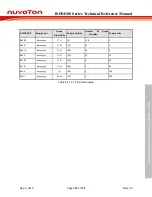
Page 103: ...pt 23 7 Reserved Reserved 24 8 WDT_INT Watchdog Timer interrupt 25 9 WWDT_INT Window Watchdog Timer interrupt 26 10 EINT0 External interrupt 27 11 EINT1 External interrupt 28 12 EINT2 External interru...

Page 104: ...54 38 I2C0_INT I2C0 interrupt 55 39 I2C1_INT I2C1 interrupt 56 40 PDMA_INT PDMA interrupt 57 41 Reserved Reserved 58 42 EADC0_INT EADC interrupt source 0 59 43 EADC1_INT EADC interrupt source 1 60 44...

Page 105: ...ve state until cleared by reset or an exception return Clearing the enable bit prevents new activations of the associated interrupt NVIC interrupts can be pended un pended using a complementary pair o...

Page 106: ...W IRQ32 IRQ63 Set Pending Control Register 0x0000_0000 NVIC_ISPR2 0xE000E208 R W IRQ64 IRQ95 Set Pending Control Register 0x0000_0000 NVIC_ICPR0 0xE000E280 R W IRQ0 IRQ31 Clear Pending Control Registe...

Page 107: ...E000E100 R W IRQ0 IRQ31 Set Enable Control Register 0x0000_0000 31 30 29 28 27 26 25 24 SETENA 23 22 21 20 19 18 17 16 SETENA 15 14 13 12 11 10 9 8 SETENA 7 6 5 4 3 2 1 0 SETENA Bits Description 31 0...

Page 108: ...E000E104 R W IRQ32 IRQ63 Set Enable Control Register 0x0000_0000 31 30 29 28 27 26 25 24 SETENA 23 22 21 20 19 18 17 16 SETENA 15 14 13 12 11 10 9 8 SETENA 7 6 5 4 3 2 1 0 SETENA Bits Description 31 0...

Page 109: ...E000E108 R W IRQ64 IRQ95 Set Enable Control Register 0x0000_0000 31 30 29 28 27 26 25 24 SETENA 23 22 21 20 19 18 17 16 SETENA 15 14 13 12 11 10 9 8 SETENA 7 6 5 4 3 2 1 0 SETENA Bits Description 31 0...

Page 110: ...00E180 R W IRQ0 IRQ31 Clear Enable Control Register 0x0000_0000 31 30 29 28 27 26 25 24 CALENA 23 22 21 20 19 18 17 16 CALENA 15 14 13 12 11 10 9 8 CALENA 7 6 5 4 3 2 1 0 CALENA Bits Description 31 0...

Page 111: ...00E184 R W IRQ32 IRQ63 Clear Enable Control Register 0x0000_0000 31 30 29 28 27 26 25 24 CALENA 23 22 21 20 19 18 17 16 CALENA 15 14 13 12 11 10 9 8 CALENA 7 6 5 4 3 2 1 0 CALENA Bits Description 31 0...

Page 112: ...00E188 R W IRQ64 IRQ95 Clear Enable Control Register 0x0000_0000 31 30 29 28 27 26 25 24 CALENA 23 22 21 20 19 18 17 16 CALENA 15 14 13 12 11 10 9 8 CALENA 7 6 5 4 3 2 1 0 CALENA Bits Description 31 0...

Page 113: ...et Pending Control Register 0x0000_0000 31 30 29 28 27 26 25 24 SETPEND 23 22 21 20 19 18 17 16 SETPEND 15 14 13 12 11 10 9 8 SETPEND 7 6 5 4 3 2 1 0 SETPEND Bits Description 31 0 SETPEND Interrupt Se...

Page 114: ...Set Pending Control Register 0x0000_0000 31 30 29 28 27 26 25 24 SETPEND 23 22 21 20 19 18 17 16 SETPEND 15 14 13 12 11 10 9 8 SETPEND 7 6 5 4 3 2 1 0 SETPEND Bits Description 31 0 SETPEND Interrupt S...

Page 115: ...Set Pending Control Register 0x0000_0000 31 30 29 28 27 26 25 24 SETPEND 23 22 21 20 19 18 17 16 SETPEND 15 14 13 12 11 10 9 8 SETPEND 7 6 5 4 3 2 1 0 SETPEND Bits Description 31 0 SETPEND Interrupt S...

Page 116: ...ear Pending Control Register 0x0000_0000 31 30 29 28 27 26 25 24 CALPEND 23 22 21 20 19 18 17 16 CALPEND 15 14 13 12 11 10 9 8 CALPEND 7 6 5 4 3 2 1 0 CALPEND Bits Description 31 0 CALPEND Interrupt C...

Page 117: ...lear Pending Control Register 0x0000_0000 31 30 29 28 27 26 25 24 CALPEND 23 22 21 20 19 18 17 16 CALPEND 15 14 13 12 11 10 9 8 CALPEND 7 6 5 4 3 2 1 0 CALPEND Bits Description 31 0 CALPEND Interrupt...

Page 118: ...lear Pending Control Register 0x0000_0000 31 30 29 28 27 26 25 24 CALPEND 23 22 21 20 19 18 17 16 CALPEND 15 14 13 12 11 10 9 8 CALPEND 7 6 5 4 3 2 1 0 CALPEND Bits Description 31 0 CALPEND Interrupt...

Page 119: ...R W Description Reset Value NVIC_IABR0 0xE000E300 R W IRQ0 IRQ31 Active Bit Register 0x0000_0000 31 30 29 28 27 26 25 24 ACTIVE 23 22 21 20 19 18 17 16 ACTIVE 15 14 13 12 11 10 9 8 ACTIVE 7 6 5 4 3 2...

Page 120: ...R W Description Reset Value NVIC_IABR1 0xE000E304 R W IRQ32 IRQ63 Active Bit Register 0x0000_0000 31 30 29 28 27 26 25 24 ACTIVE 23 22 21 20 19 18 17 16 ACTIVE 15 14 13 12 11 10 9 8 ACTIVE 7 6 5 4 3...

Page 121: ...R W Description Reset Value NVIC_IABR2 0xE000E308 R W IRQ64 IRQ95 Active Bit Register 0x0000_0000 31 30 29 28 27 26 25 24 ACTIVE 23 22 21 20 19 18 17 16 ACTIVE 15 14 13 12 11 10 9 8 ACTIVE 7 6 5 4 3...

Page 122: ...priority 27 24 Reserved Reserved Any values read should be ignored When writing to this field always write with reset value 23 20 PRI_4n_2 Priority of IRQ_4n 2 0 denotes the highest priority and 15 d...

Page 123: ...23 22 21 20 19 18 17 16 Reserved 15 14 13 12 11 10 9 8 Reserved INTID 7 6 5 4 3 2 1 0 INTID Bits Description 31 9 Reserved Reserved Any values read should be ignored When writing to this field always...

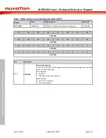
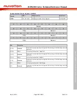
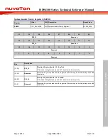
Page 124: ...CE MANUAL 6 2 13 4 NMI Control Registers R read only W write only R W both read and write Register Offset R W Description Reset Value NMI Base Address NMI_BA 0x4000_0300 NMIEN NMI_BA 0x00 R W NMI Sour...

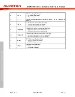
Page 125: ...MI Source Enable Write Protect 0 External interrupt 5 NMI source Disabled 1 External interrupt 5 NMI source Enabled Note This bit is write protected Refer to the SYS_REGLCTL register 12 EINT4 External...

Page 126: ...otected 0 Clock fail detected interrupt NMI source Disabled 1 Clock fail detected interrupt NMI source Enabled Note This bit is write protected Refer to the SYS_REGLCTL register 3 SRAM_PERR SRAM Parit...

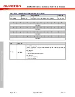
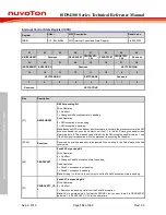
Page 127: ...rupt 5 Interrupt Flag Read Only 0 External Interrupt 5 interrupt is deasserted 1 External Interrupt 5 interrupt is asserted 12 EINT4 External Interrupt 4 Interrupt Flag Read Only 0 External Interrupt...

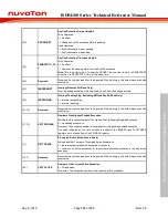
Page 128: ...cted interrupt is deasserted 1 Clock fail detected interrupt is asserted 3 SRAM_PERR SRAM Parity Check Error Interrupt Flag Read Only 0 SRAM parity check error interrupt is deasserted 1 SRAM parity ch...

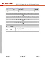
Page 129: ...ERIES TECHNICAL REFERENCE MANUAL 6 2 13 5 AHB Bus Matrix Priority Control Register R read only W write only R W both read and write Register Offset R W Description Reset Value AHB Base Address AHB_BA...

Page 130: ...22 21 20 19 18 17 16 Reserved 15 14 13 12 11 10 9 8 Reserved 7 6 5 4 3 2 1 0 Reserved INTACTEN Bits Description 31 1 Reserved Reserved Any values read should be ignored When writing to this field alwa...

Page 131: ...e Address SCS_BA 0xE000_E000 ICSR SCS_BA 0xD04 R W Interrupt Control and State Register 0x0000_0000 AIRCR SCS_BA 0xD0C R W Application Interrupt and Reset Control Register 0xFA05_0000 SCR SCS_BA 0xD10...

Page 132: ...rity exception normally the processor enters the NMI exception handler as soon as it detects a write of 1 to this bit Entering the handler then clears this bit to 0 This means a read of this bit by th...

Page 133: ...ding NMI and Faults Read Only 0 Interrupt not pending 1 Interrupt pending 21 18 Reserved Reserved Any values read should be ignored When writing to this field always write with reset value 17 12 VECTP...

Page 134: ...a Endianness 0 Little endian 1 Big endian 14 11 Reserved Reserved Any values read should be ignored When writing to this field always write with reset value 10 8 PRIGROUP Interrupt Priority Grouping T...

Page 135: ...p Priority Bits Subpriority Bits Number Of Group Priorities Subpriorities 0b000 bxxxxxxx y 7 1 0 128 2 0b001 bxxxxxx yy 7 2 1 0 64 4 0b010 bxxxxx yyy 7 3 2 0 32 8 0b011 bxxxx yyyy 7 4 3 0 16 16 0b100...

Page 136: ...event or interrupt enters pending state the event signal wakes up the processor from WFE If the processor is not waiting for an event the event is registered and affects the next WFE The processor als...

Page 137: ...Description 31 24 Reserved Reserved Any values read should be ignored When writing to this field always write with reset value 23 20 PRI_6 Priority of system handler 6 UsageFault 19 16 Reserved Reser...

Page 138: ...W System Handler Priority Register 2 0x0000_0000 31 30 29 28 27 26 25 24 PRI_11 Reserved 23 22 21 20 19 18 17 16 Reserved 15 14 13 12 11 10 9 8 Reserved 7 6 5 4 3 2 1 0 Reserved Bits Description 31 2...

Page 139: ...Reserved 15 14 13 12 11 10 9 8 Reserved 7 6 5 4 3 2 1 0 Reserved Bits Description 31 28 PRI_15 Priority of System Handler 15 SysTick 0 denotes the highest priority and 0xF denotes the lowest priority...

Page 140: ...k source selection and a clock divider The chip will not enter Power down mode until CPU sets the Power down enable bit PDEN CLK_PWRCTL 7 and Cortex M4 core executes the WFI instruction After that chi...

Page 141: ...LKSEL3 8 10000 CLK_CLKSEL2 3 2 CLK_CLKSEL2 7 6 PCLK0 HXT HIRC PLLFOUT 11 10 01 00 1 SPI0_CLKDIV 8 0 1 1 SPI2_CLKDIV 8 0 1 SPI0 SPI2 CLK_CLKSEL2 5 4 PCLK1 HXT HIRC PLLFOUT 11 10 01 00 1 SPI1_CLKDIV 8 0...

Page 142: ...an be selected from external 4 24 576 MHz external high speed crystal HXT or internal high speed oscillator HIRC Selectable 48 0 MHz or 49 152 MHz internal high speed RC oscillator HIRC 10 kHz interna...

Page 143: ...t control If HXT failure detector is enabled the HIRC clock will be also enabled automatically The clock controller will automatically switch the system clock HCLK source from HXT to HIRC if the follo...

Page 144: ...O Figure 6 3 4 HXT Stop Protect Procedure The SysTick clock source can be from CPU clock or external reference clock determined by CLKSRC bit SYST_CTRL 2 If CLKSRC 1 CPU core clock is used for SysTick...

Page 145: ...f 2 frequency divider which is composed of 16 chained divide by 2 shift registers One of the 16 shift register outputs selected by a sixteen to one multiplexer is reflected to CLKO function pin Theref...

Page 146: ...NICAL REFERENCE MANUAL 6 3 7 Clock Setting Limitation The maximum frequency of PCLK0 and PCLK1 is 90 MHz If the frequency of HCLK greater than 90 MHz the APB1DIV CLK_PCLKDIV 6 4 and APB0DIV CLK_PCLKDI...

Page 147: ...0 CLK_PCLKDIV CLK_BA 0x34 R W APB Clock Divider Register 0x0000_0000 CLK_PLLCTL CLK_BA 0x40 R W PLL Control Register 0x0005_8430 CLK_STATUS CLK_BA 0x50 R Clock Status Monitor Register 0x0000_0018 CLK_...

Page 148: ...by Power down Control Register 0x0000_0000 Note 1 Any register not listed here is reserved and must not be written The result of a read operation on these bits is undefined 2 The reserved register fie...

Page 149: ...BO mode disabled 1 HXT Crystal TURBO mode enabled 12 HXTSELTYP HXT Crystal Type Select Bit Write Protected This is a protected register Please refer to open lock sequence to program it 0 Select INV ty...

Page 150: ...up source is occurred Refer Power Modes and Wake up Sources chapter Note1 Write 1 to clear the bit to 0 Note2 This bit works only if PDWKIEN CLK_PWRCTL 5 set to 1 5 PDWKIEN Power down Mode Wake up In...

Page 151: ...bit is write protected Refer to the SYS_REGLCTL register Note 2 The reset value of this bit is 0 0 HXTEN HXT Enable Bit Write Protected The bit default value is set by flash controller user configura...

Page 152: ...rite with reset value 15 FMCIDLE Flash Memory Controller Clock Enable Bit in IDLE Mode 0 FMC clock Disabled when chip is under IDLE mode 1 FMC clock Enabled when chip is under IDLE mode 14 8 Reserved...

Page 153: ...N TMR0CKEN RTCCKEN WDTCKEN Bits Description 31 30 Reserved Reserved Any values read should be ignored When writing to this field always write with reset value 29 I2S0CKEN I2 S0 Clock Enable Bit 0 I2 S...

Page 154: ...clock Enabled 5 TMR3CKEN Timer3 Clock Enable Bit 0 Timer3 clock Disabled 1 Timer3 clock Enabled 4 TMR2CKEN Timer2 Clock Enable Bit 0 Timer2 clock Disabled 1 Timer2 clock Enabled 3 TMR1CKEN Timer1 Clo...

Page 155: ...23 22 21 20 19 18 17 16 Reserved PWM0CKEN 15 14 13 12 11 10 9 8 Reserved 7 6 5 4 3 2 1 0 Reserved DPWMCKEN Reserved Bits Description 31 17 Reserved Reserved Any values read should be ignored When wri...

Page 156: ...CTL register 23 6 Reserved Reserved Any values read should be ignored When writing to this field always write with reset value 5 3 STCLKSEL Cortex M4 SysTick Clock Source Selection Write Protected If...

Page 157: ...57 of 928 Rev1 09 ISD94100 SERIES TECHNICAL REFERENCE MANUAL 001 Clock source from LXT 010 Clock source from PLL 011 Clock source from LIRC 111 Clock source from HIRC Other Reserved Do not use Note Th...

Page 158: ...9 28 CLKOSEL Clock Divider Clock Source Selection 00 Clock source from external high speed crystal oscillator HXT 01 Clock source from external low speed crystal oscillator LXT 10 Clock source from HC...

Page 159: ...ck source from external low speed crystal oscillator LXT 010 Clock source from PCLK0 011 Clock source from external clock TM1 pin 101 Clock source from internal low speed RC oscillator LIRC 111 Clock...

Page 160: ...EL DPWM Clock Source Selection 00 Clock source from external high speed crystal oscillator HXT 01 Clock source from PLL 10 Clock source from PCLK0 11 Clock source from internal high speed RC oscillato...

Page 161: ...ck source from external high speed crystal oscillator HXT 01 Clock source from PLL 10 Clock source from PCLK0 11 Clock source from internal high speed RC oscillator HIRC 1 Reserved Reserved Any values...

Page 162: ...scription 31 18 Reserved Reserved Any values read should be ignored When writing to this field always write with reset value 17 16 I2S0SEL I2 S0 Clock Source Selection 00 Clock source from external hi...

Page 163: ...read should be ignored When writing to this field always write with reset value 23 16 EADCDIV EADC Clock Divide Number From EADC Clock Source EADC clock frequency EADC clock source frequency EADCDIV...

Page 164: ...31 30 29 28 27 26 25 24 Reserved USBSEL 23 22 21 20 19 18 17 16 Reserved 15 14 13 12 11 10 9 8 Reserved 7 6 5 4 3 2 1 0 Reserved Bits Description 31 25 Reserved Reserved Any values read should be igno...

Page 165: ...IV APB1 Clock Divider APB1 clock can be divided from HCLK 000 PCLK1 HCLK 001 PCLK1 1 2 HCLK 010 PCLK1 1 4 HCLK 011 PCLK1 1 8 HCLK 100 PCLK1 1 16 HCLK Others Reserved Do not use Note When the clock rat...

Page 166: ...e for source clock is larger than 12 MHz Note This bit is write protected Refer to the SYS_REGLCTL register 22 20 Reserved Reserved Any values read should be ignored When writing to this field always...

Page 167: ...he SYS_REGLCTL register 8 0 FBDIV PLL Feedback Divider Control Write Protected Refer to the formulas below the table Note This bit is write protected Refer to the SYS_REGLCTL register Output Clock Fre...

Page 168: ...ource CLK_CLKSEL0 2 0 If switch target clock is stable this bit will be set to 0 If switch target clock is not stable this bit will be set to 1 0 Clock switching success 1 Clock switching failure 6 5...

Page 169: ...Manual Sep 9 2019 Page 169 of 928 Rev1 09 ISD94100 SERIES TECHNICAL REFERENCE MANUAL 0 External high speed crystal oscillator HXT clock is not stable or disabled 1 External high speed crystal oscilla...

Page 170: ...g to this field always write with reset value 6 CLK1HZEN Clock Output 1Hz Enable Bit 0 1 Hz clock output for RTC frequency compensation Disabled 1 1 Hz clock output for RTC frequency compensation Enab...

Page 171: ...ed 16 HXTFQDEN HXT Clock Frequency Monitor Enable Bit 0 External high speed crystal oscillator HXT clock frequency Range Detector Disabled 1 External high speed crystal oscillator HXT clock frequency...

Page 172: ...IES TECHNICAL REFERENCE MANUAL 0 External high speed crystal oscillator HXT clock fail detector Disabled 1 External high speed crystal oscillator HXT clock fail detector Enabled 3 0 Reserved Reserved...

Page 173: ...with reset value 8 HXTFQIF HXT Clock Frequency Range Detector Interrupt Flag 0 External high speed crystal oscillator HXT clock frequency is normal 1 External high speed crystal oscillator HXT clock...

Page 174: ...5 14 13 12 11 10 9 8 Reserved UPERBD 7 6 5 4 3 2 1 0 UPERBD Bits Description 31 10 Reserved Reserved Any values read should be ignored When writing to this field always write with reset value 9 0 UPER...

Page 175: ...14 13 12 11 10 9 8 Reserved LOWERBD 7 6 5 4 3 2 1 0 LOWERBD Bits Description 31 10 Reserved Reserved Any values read should be ignored When writing to this field always write with reset value 9 0 LOW...

Page 176: ...ter 22 20 Reserved Reserved Any values read should be ignored When writing to this field always write with reset value 19 BODSPWK BOD Standby Power down Mode Wake up Enable Write Protected This is a p...

Page 177: ...cted Refer to the SYS_REGLCTL register 8 WKTMREN Wake up Timer Enable Write Protected This is a protected register Please refer to open lock sequence to program it 0 Wake up timer disable at DPD SPD m...

Page 178: ...roup pins This flag is cleared when SPD mode is entered 10 GPCWK GPC Wake up Flag Read Only This flag indicates that wake up of chip from Standby Power down mode was requested by a transition of selec...

Page 179: ...Reserved Any values read should be ignored When writing to this field always write with reset value 2 DPD_TMRWK DPD Mode Wake up Timer Wake up Flag Read Only This flag indicates that wake up of chip...

Page 180: ...9 18 17 16 Reserved 15 14 13 12 11 10 9 8 Reserved OVEN 7 6 5 4 3 2 1 0 Reserved Bits Description 31 9 Reserved Reserved Any values read should be ignored When writing to this field always write with...

Page 181: ...mpling Cycle Selection 0000 Sample wake up input once per 1 clocks 0001 Sample wake up input once per 2 clocks 0010 Sample wake up input once per 4 clocks 0011 Sample wake up input once per 8 clocks 0...

Page 182: ...sampled by continuous two de bounce sample cycle the input signal transition is seen as the signal bounce and will not trigger the wakeup The de bounce clock source is the internal low speed RC oscil...

Page 183: ...e with reset value 2 PFWKEN Pin Falling Edge Wake up Enable Bit 0 PA group pin falling edge wake up function disabled 1 PA group pin falling edge wake up function enabled 1 PRWKEN Pin Rising Edge Wake...

Page 184: ...e width cannot be sampled by continuous two de bounce sample cycle the input signal transition is seen as the signal bounce and will not trigger the wakeup The de bounce clock source is the internal l...

Page 185: ...e with reset value 2 PFWKEN Pin Falling Edge Wake up Enable Bit 0 PB group pin falling edge wake up function disabled 1 PB group pin falling edge wake up function enabled 1 PRWKEN Pin Rising Edge Wake...

Page 186: ...sampled by continuous two de bounce sample cycle the input signal transition is seen as the signal bounce and will not trigger the wakeup The de bounce clock source is the internal low speed RC oscil...

Page 187: ...e with reset value 2 PFWKEN Pin Falling Edge Wake up Enable Bit 0 PC group pin falling edge wake up function disabled 1 PC group pin falling edge wake up function enabled 1 PRWKEN Pin Rising Edge Wake...

Page 188: ...sampled by continuous two de bounce sample cycle the input signal transition is seen as the signal bounce and will not trigger the wakeup The de bounce clock source is the internal low speed RC oscil...

Page 189: ...e with reset value 2 PFWKEN Pin Falling Edge Wake up Enable Bit 0 PD group pin falling edge wake up function disabled 1 PD group pin falling edge wake up function enabled 1 PRWKEN Pin Rising Edge Wake...

Page 190: ...rved 23 22 21 20 19 18 17 16 Reserved 15 14 13 12 11 10 9 8 Reserved 7 6 5 4 3 2 1 0 Reserved IOHR Bits Description 31 1 Reserved Reserved Any values read should be ignored When writing to this field...

Page 191: ...N in CONFIG0 and data flash base address DFBA in CONFIG1 When DFEN is set to 1 the data flash size is zero When DFEN is set to 0 the APROM and data flash share 512 KB continuous address and the start...

Page 192: ...logic The block diagram of flash memory controller is shown as follows Flash Operation Controller Flash Initialization Controller AHB Slave Interface Embedded Flash Memory Flash Control Registers Cac...

Page 193: ...description follows Flash Initialization Controller When chip is powered on or resumes active from reset the flash initialization controller will start to access flash automatically and check the fla...

Page 194: ...ROM Application data Figure 6 4 2 Memory Organization APROM and Data Flash APROM is main memory for user applications Data Flash is used to store application parameters not instruction Data Flash is...

Page 195: ...Note N is the page number of configured data flash One page size is 4096 bytes N 0 Table 6 4 4 1 Flash Memory Address Map 6 4 4 2 Boot Configuration Typically the system vector table is located in RO...

Page 196: ...ector values from LDROM space 0x0010_0100 to 0x0010_01FF In this mode the MCU boots from LDROM and has the access to all memory space including 512KB APROM and 4KB LDROM The device can read erase and...

Page 197: ...g can be done by first writing the target remap to address to FMC_ISPADDR register and then triggering ISP procedure with the Vector Remap command 0x2E The targeted remapping address needs to be in al...

Page 198: ...DROM has only 4 KB one page size In this mode remapping is not supported 6 4 4 2 4 Boot from APROM without IAP support By writing 0b11 into CBS 1 0 bits in CONFIG0 the ISD94100 device will load the sy...

Page 199: ...performed without removing the microcontroller from the system by writing data and ISP commands to the device through the on chip connectivity interface such as UART I2C or SPI See Table 6 4 4 3 ISP...

Page 200: ...x0000_0000 FMC_ISPDAT 0x0000_00DA FMC_MPDAT0 FMC_MPDAT3 N A Read Device ID 0x0C 0x0000_0000 FMC_ISPDAT Return Device ID FMC_MPDAT0 FMC_MPDAT3 N A Read CRC32 Checksum 0x0D 0x0000_0000 FMC_ISPDAT Return...

Page 201: ...d information Figure 6 4 8 illustrates the ISP flow Configure FMC_ISPCTL register to decide to which part of flash memory to update LDROM APROM or configuration bytes Writing 1 to ISPEN FMC_ISPCTL 0 e...

Page 202: ...ny read or write operation the ISPEN bit in FMC_ISPCTRL register needs to be enabled and after operation finishes ISPEN bit needs to be disabled for the purpose of data security For more detailed info...

Page 203: ...de for 64 bit read is 0x40 FMC ISPADDR u32addr FMC ISPDAT 0x0 FMC ISPTRG FMC_ISPTRG_ISPGO_Msk set ISPGO bit to start reading while FMC ISPSTS FMC_ISPSTS_ISPBUSY_Msk u32data0 FMC MPDAT0 u32data1 FMC MP...

Page 204: ...nd FMC_MPDAT1 for MSB word The ISP command is 0x61 Enable ISPEN Set ISPGO 1 End of ISP Operation Check ISPFF 1 YES End of Flash Operation NO Set PT Write FMC_ISPADDR Write FMC_ISPCMD Write FMC_MPDAT0...

Page 205: ...LD TIME SETUP TIME fix 8 bytes programming HOLD TIME SETUP TIME 16 512 bytes programming 16 bytes align HOLD TIME Time Figure 6 4 11 Timeline comparison for write operations Within a multi word progra...

Page 206: ...should put on FMC_MPDAT2 and 2nd word is FMC_MPDAT3 3rd word is FMC_MPDAT0 and 4th word is FMC_MPDAT1 The maximum programming size is 512 bytes and aligns to 512 byte address While FMC controller per...

Page 207: ...ite FMC_MPDAT2 Write FMC_MPDAT3 Y N Enable ISPEN Set ISPGO 1 End of ISP Operation Y Programming Finish Read FMC_MPSTS MPBUSY 0 N Y Write FMC_MPDAT0 Write FMC_MPDAT1 Read FMC_MPSTS N Y MPBUSY 0 N Y Wri...

Page 208: ...will be kept until cleared by software or a new erase operation The ISD94100 series flash programing with self verification feature is shown in Figure 6 4 14 below Traditional Flash Programming Start...

Page 209: ...he high voltage requirement for flash programming is not suitable for continuous fast programming 6 4 4 7 CRC32 Checksum Calculation The ISD94100 series supports the CRC32 checksum calculation functio...

Page 210: ...FF after a APROM or LDROM flash erase operation Two or Three steps complete this flash all one verification Two step flow Step 1 perform ISP Run Flash All One Verification operation Step 2 read ALLONE...

Page 211: ...ISD94100 Series Technical Reference Manual Sep 9 2019 Page 211 of 928 Rev1 09 ISD94100 SERIES TECHNICAL REFERENCE MANUAL while FMC ISPSTS FMC_ISPSTS_ISPBUSY_Msk...

Page 212: ...ing trigger events include HCLKSEL CLK_CLKSEL0 CLK_PLLCTL and HCLKDIV CLK_CLKDIV0 When detecting a event FMC will set the max number i e 8 temporarily to CYCLE FMC_CYCCTL 3 0 register to save flash ac...

Page 213: ...s Cycle The optimized access cycle number YES YES YES NO NO NO Figure 6 4 17 Flash access cycle auto tuning flow 6 4 4 10 Lock Effect Tables The ISD94100 series supports four kinds of protections incl...

Page 214: ...memory via ISP registers can modify registers and SRAM YES YES YES YES Accept ICP mass erase command YES YES YES YES SWD ICE can use page erase program read flash memory by ICP YES NO YES NO SWD ICE...

Page 215: ...00 R W ISP Control Register 0x0000_0000 FMC_ISPADDR FMC_BA 0x04 R W ISP Address Register 0x0000_0000 FMC_ISPDAT FMC_BA 0x08 R W ISP Data Register 0x0000_0000 FMC_ISPCMD FMC_BA 0x0C R W ISP Command Reg...

Page 216: ...Page 216 of 928 Rev1 09 ISD94100 SERIES TECHNICAL REFERENCE MANUAL 2 The reserved register fields that listed in register description must be written to their reset value Writing reserved fields with...

Page 217: ...are enable function is inactive Others WDT hardware enable function is active WDT clock is always on 30 28 Reserved Reserved bit should always be programmed with 1 27 CFGXT1 XTAL Multi Function Select...

Page 218: ...ode 01 Boot from LDROM without IAP mode 10 Boot from APROM with IAP mode 11 Boot from APROM without IAP mode Note BS FMC_ISPCTL 1 is only be used to control boot switching when CBS 0 1 VECMAP FMC_ISPS...

Page 219: ...94100 SERIES TECHNICAL REFERENCE MANUAL 0 DFEN Data Flash Enable Bit The Data Flash is shared with APROM and the base address of Data Flash is decided by DFBA CONFIG1 19 0 when DFEN is 0 0 Data Flash...

Page 220: ...14 13 12 11 10 9 8 DFBA 7 6 5 4 3 2 1 0 DFBA Bits Descriptions 31 20 Reserved Reserved bit should always be programmed with 0 19 0 DFBA Data Flash Base Address This register works only when DFEN CONFI...

Page 221: ...ed with 1 15 0 ALOCK Advance Security Lock Control Must be set to 0x5A5A for access to flash memory content Any other value flash memory is locked To unlock system a whole chip erase must be performed...

Page 222: ...When writing to this field always write with reset value 6 ISPFF ISP Fail Flag Write Protected This bit is set by hardware when a triggered ISP meets any of the following conditions 1 APROM writes to...

Page 223: ...also functions as chip booting status flag which can be used to check where chip booted from This bit is initiated with the inversed value of CBS in CONFIG0 after any reset is happened except CPU rese...

Page 224: ...Address The ISD94100 series is equipped with an embedded ISPADDR 1 0 must be kept 00 for ISP 32 bit operation ISPADDR 2 0 must be kept 000 for ISP 64 bit operation ISPADDR 3 0 must be kept 0000 for IS...

Page 225: ...9 8 ISPDAT 7 6 5 4 3 2 1 0 ISPDAT Bits Description 31 0 ISPDAT ISP Data Write data to this register before ISP program operation Read data from this register after ISP read operation When ISPFF FMC_IS...

Page 226: ...values read should be ignored When writing to this field always write with reset value 6 0 CMD ISP Command ISP command table is shown below 0x00 FLASH Read 0x04 Read Unique ID 0x08 Read Flash All One...

Page 227: ...22 21 20 19 18 17 16 Reserved 15 14 13 12 11 10 9 8 Reserved 7 6 5 4 3 2 1 0 Reserved ISPGO Bits Description 31 1 Reserved Reserved Any values read should be ignored When writing to this field always...

Page 228: ...FMC_BA 0x14 R Data Flash Base Address 0xXXXX_XXXX 31 30 29 28 27 26 25 24 DFBA 23 22 21 20 19 18 17 16 DFBA 15 14 13 12 11 10 9 8 DFBA 7 6 5 4 3 2 1 0 DFBA Bits Description 31 0 DFBA Data Flash Base A...

Page 229: ...ash All One Verification complete this bit also can be clear by writing 1 0 All of flash bits are 1 after Run Flash All One Verification complete 1 Flash bits are not all 1 after Run Flash All One Ver...

Page 230: ...d When writing to this field always write with reset value 2 1 CBS Chip Boot Selection Mode Read Only This CBS field is just a copy of flash controller user configuration register CBS CONFIG0 7 6 Note...

Page 231: ...erved FADIS 7 6 5 4 3 2 1 0 Reserved CYCLE Bits Description 31 9 Reserved Reserved Any values read should be ignored When writing to this field always write with reset value 8 FADIS Flash Access Cycle...

Page 232: ...frequency range is 27 54 MHz 0011 CPU access with three wait cycles if cache miss flash access cylcle is 3 The optimized HCLK working frequency range is 54 81 MHz 0100 CPU access with four wait cycles...

Page 233: ...ue FMC_MPDAT0 FMC_BA 0x80 R W ISP Multi Word Program Data0 Register 0x0000_0000 31 30 29 28 27 26 25 24 ISPDAT0 23 22 21 20 19 18 17 16 ISPDAT0 15 14 13 12 11 10 9 8 ISPDAT0 7 6 5 4 3 2 1 0 ISPDAT0 Bi...

Page 234: ...egister Offset R W Description Reset Value FMC_MPDAT1 FMC_BA 0x84 R W ISP Multi Word Program Data1 Register 0x0000_0000 31 30 29 28 27 26 25 24 ISPDAT1 23 22 21 20 19 18 17 16 ISPDAT1 15 14 13 12 11 1...

Page 235: ...T2 Register Offset R W Description Reset Value FMC_MPDAT2 FMC_BA 0x88 R W ISP Multi Word Program Data2 Register 0x0000_0000 31 30 29 28 27 26 25 24 ISPDAT2 23 22 21 20 19 18 17 16 ISPDAT2 15 14 13 12...

Page 236: ...T3 Register Offset R W Description Reset Value FMC_MPDAT3 FMC_BA 0x8C R W ISP Multi Word Program Data3 Register 0x0000_0000 31 30 29 28 27 26 25 24 ISPDAT3 23 22 21 20 19 18 17 16 ISPDAT3 15 14 13 12...

Page 237: ...n written and not program to flash complete 6 D2 ISP DATA 2 Flag Read Only This bit is set when FMC_MPDAT2 is written and auto clear to 0 when the FMC_MPDAT2 data is programmed to flash complete 0 FMC...

Page 238: ...to 0 4 Page Erase command at LOCK mode with ICE connection 5 Erase or Program command at brown out detected 6 Destination address is illegal such as over an available range 7 Invalid ISP commands 1 P...

Page 239: ...FMC_MPADDR FMC_BA 0xC4 R ISP Multi Word Program Address Status Register 0x0000_0000 31 30 29 28 27 26 25 24 MPADDR 23 22 21 20 19 18 17 16 MPADDR 15 14 13 12 11 10 9 8 MPADDR 7 6 5 4 3 2 1 0 MPADDR Bi...

Page 240: ...except PA 8 PA 8 pin default I O mode is determined by GPA8_LOW bit CONFIG0 11 Every I O pin has a weak pull up resistor with value 50 k when I O pin configured as quasi bidirectional output low 6 5...

Page 241: ...ol Register Control Registers Interrupt Wake up Event Detector PB 15 13 9 0 PC 15 0 PD 15 0 GPIO_INT Figure 6 5 1 GPIO Controller Block Diagram 6 5 4 Basic Configuration Reset configuration Writing 1...

Page 242: ...onding Px n pin in in Push pull Output mode and the pin supports digital output function with source sink current capability As shown in Figure 6 5 2 the bit value in the corresponding DOUT Px_DOUT n...

Page 243: ...pin architecture Port Pin Port Pin N N P P VDD VDD Port Latch Data Port Latch Data Input Data Input Data 2 CPU Clock Delay P P Strong Strong Very Weak Very Weak Figure 6 5 4 Quasi Bidirectional I O M...

Page 244: ...generated when a valid high pin status is met If the pin status was high before DBEN Px_DBEN is enabled an interrupt can only happen after first a valid low status detected and then a valid high statu...

Page 245: ...e condition for de bounce support System Status DBEN DBCLKSRC Description Normal Mode Idle Mode 0 0 No de bounce function 1 No de bounce function 1 0 De bounce function using HCLK 1 De bounce function...

Page 246: ...nd Pull down Selection Register 0x0000_0000 PB_MODE GPIO_BA 0x040 R W PB I O Mode Control 0xXX0X_XXXX PB_DINOFF GPIO_BA 0x044 R W PB Digital Input Path Disable Control 0x0000_0000 PB_DOUT GPIO_BA 0x04...

Page 247: ...0 PD_INTTYPE GPIO_BA 0x0D8 R W PD Interrupt Trigger Type Control 0x0000_0000 PD_INTEN GPIO_BA 0x0DC R W PD Interrupt Enable Control Register 0x0000_0000 PD_INTSRC GPIO_BA 0x0E0 R W PD Interrupt Source...

Page 248: ...O Pin n Mode Control Determine each I O mode of Px n pins 00 Px n is in Input mode 01 Px n is in Push pull Output mode 10 Px n is in Open drain Output mode 11 Px n is in Quasi bidirectional mode Note...

Page 249: ...Disable Control 0x0000_0000 31 30 29 28 27 26 25 24 DINOFF 23 22 21 20 19 18 17 16 DINOFF 15 14 13 12 11 10 9 8 Reserved 7 6 5 4 3 2 1 0 Reserved Bits Description n 16 n 0 1 15 DINOFF n Port A D Pin...

Page 250: ...alue n n 0 1 15 DOUT n Port A D Pin n Output Value Each of these bits controls the status of a Px n pin when the Px n is configured as Push pull output Open drain output or Quasi bidirectional mode 0...

Page 251: ...11 10 9 8 DATMSK 7 6 5 4 3 2 1 0 DATMSK Bits Description 31 8 Reserved Reserved Any values read should be ignored When writing to this field always write with reset value n n 0 1 15 DATMSK n Port A D...

Page 252: ...31 30 29 28 27 26 25 24 Reserved 23 22 21 20 19 18 17 16 Reserved 15 14 13 12 11 10 9 8 PIN 7 6 5 4 3 2 1 0 PIN Bits Description 31 16 Reserved Reserved Any values read should be ignored When writing...

Page 253: ...6 Reserved Reserved Any values read should be ignored When writing to this field always write with reset value n n 0 1 15 DBEN n Port A D Pin n Input Signal De bounce Enable Bit The DBEN n bit is used...

Page 254: ...g to this field always write with reset value n n 0 1 15 TYPE n Port A D Pin n Edge or Level Detection Interrupt Trigger Type Control TYPE Px_INTTYPE n bit is used to control the triggered interrupt i...

Page 255: ...is level trigger TYPE Px_INTTYPE n bit is set to 1 the input Px n pin will generate the interrupt while this pin state is at high level If the interrupt is edge trigger TYPE Px_INTTYPE n bit is set t...

Page 256: ...ISD94100 Series Technical Reference Manual Sep 9 2019 Page 256 of 928 Rev1 09 ISD94100 SERIES TECHNICAL REFERENCE MANUAL Max n 15 for port A C D n 0 9 13 14 15 for port B...

Page 257: ...x0E0 R W PD Interrupt Source Flag 0x0000_0000 31 30 29 28 27 26 25 24 Reserved 23 22 21 20 19 18 17 16 Reserved 15 14 13 12 11 10 9 8 INTSRC 7 6 5 4 3 2 1 0 INTSRC Bits Description 31 16 Reserved Rese...

Page 258: ...4 R W PC Input Schmitt Trigger Enable Register 0x0000_0000 PD_SMTEN GPIO_BA 0x0E4 R W PD Input Schmitt Trigger Enable Register 0x0000_0000 31 30 29 28 27 26 25 24 Reserved 23 22 21 20 19 18 17 16 Rese...

Page 259: ...gh Slew Rate Control Register 0x0000_0000 PD_SLEWCTL GPIO_BA 0x0E8 R W PD High Slew Rate Control Register 0x0000_0000 31 30 29 28 27 26 25 24 HSREN15 HSREN14 HSREN13 HSREN12 23 22 21 20 19 18 17 16 HS...

Page 260: ...18 17 16 PUSEL11 PUSEL10 PUSEL9 PUSEL8 15 14 13 12 11 10 9 8 PUSEL7 PUSEL6 PUSEL5 PUSEL4 7 6 5 4 3 2 1 0 PUSEL3 PUSEL2 PUSEL1 PUSEL0 Bits Description 2n 1 2n n 0 1 15 PUSELn Port A D Pin n Pull up and...

Page 261: ...KSEL Bits Description 31 6 Reserved Reserved Any values read should be ignored When writing to this field always write with reset value 5 ICLKON Interrupt Clock on Mode 0 Edge detection circuit is act...

Page 262: ...interrupt input once per 16 clocks 0101 Sample interrupt input once per 32 clocks 0110 Sample interrupt input once per 64 clocks 0111 Sample interrupt input once per 128 clocks 1000 Sample interrupt...

Page 263: ...4 Reserved 23 22 21 20 19 18 17 16 Reserved 15 14 13 12 11 10 9 8 Reserved 7 6 5 4 3 2 1 0 Reserved PDIO Bits Description 31 1 Reserved Reserved Any values read should be ignored When writing to this...

Page 264: ...xed priority or round robin priority Supports transfer data width of 8 16 and 32 bits Supports source and destination address increment size can be byte half word word or no increment Supports softwar...

Page 265: ...transfer information including the transfer source address transfer destination address transfer count burst size transfer type and operation mode The Figure 6 6 2 shows the diagram of descriptor tabl...

Page 266: ...dle state OPMODE PDMA_DSCTn_CTL 1 0 0x0 and recommend user configure the descriptor table in idle state If operation mode is not in idle state user re configure channel setting may make some operation...

Page 267: ...transfer data between memory to memory without handshaking In Scatter Gather mode the table is just used for jumping to the next table entry The first task will not perform any operation transfer Fin...

Page 268: ...own in Figure 6 6 5 When loading the information is finished it will go to transfer state and start transfer by this information automatically However if the next PDMA information is also in the Scatt...

Page 269: ...ry transfers The Figure 6 6 6 shows an example about single and burst transfer type in basic mode In this example channel 1 uses single transfer type and TXCNT PDMA_DSCTn_CTL 31 16 127 Channel 0 uses...

Page 270: ...PDMA_TOUTPSC 2 4n 4n n 0 1 If time out counter counts up from 0 to corresponding channel s TOCn PDMA_TOC0_1 16 n 1 1 16n n 0 1 the PDMA controller will generate interrupt signal when corresponding TOU...

Page 271: ...ess to the PDMA_DSCTn_SA register and a source address offset count to SASOL PDMA_ASOCRn 15 0 register a destination address to the PDMA_DSCTn_DA register and a destination address offset count to DAS...

Page 272: ...ndwidth utilization is too high then FIFO overflow on peripherals can occur when PDMA request cannot be serviced in a timely manner Burst Size AHB Clock Cycles Burst Size AHB Clock Cycles 1 14 16 74 2...

Page 273: ...of PDMA Channel 2 0xXXXX_XXXX PDMA_DSCT2_DA PDMA_BA 0x28 R W Destination Address Register of PDMA Channel 2 0xXXXX_XXXX PDMA_DSCT2_NEXT PDMA_BA 0x2C R W First Scatter Gather Descriptor Table Offset Ad...

Page 274: ...PDMA_BA 0x8C R W First Scatter Gather Descriptor Table Offset Address of PDMA Channel 8 0xXXXX_XXXX PDMA_DSCT9_CTL PDMA_BA 0x90 R W Descriptor Table Control Register of PDMA Channel 9 0xXXXX_XXXX PDM...

Page 275: ...R W Descriptor Table Control Register of PDMA Channel 15 0xXXXX_XXXX PDMA_DSCT15_SA PDMA_BA 0xF4 R W Source Address Register of PDMA Channel 15 0xXXXX_XXXX PDMA_DSCT15_DA PDMA_BA 0xF8 R W Destination...

Page 276: ...x408 W PDMA Software Request Register 0x0000_0000 PDMA_TRGSTS PDMA_BA 0x40C R PDMA Channel Request Status Register 0x0000_0000 PDMA_PRISET PDMA_BA 0x410 R W PDMA Fixed Priority Setting Register 0x0000...

Page 277: ...l 2 0x0000_0000 PDMA_ASOCR2 PDMA_BA 0x514 R W Address Stride Offset Register of PDMA Channel 2 0x0000_0000 PDMA_STCR3 PDMA_BA 0x518 R W Stride Transfer Count Register of PDMA Channel 3 0x0000_0000 PDM...

Page 278: ...PDMA_DSCT8_CTL PDMA_BA 0x80 R W Descriptor Table Control Register of PDMA Channel 8 0xXXXX_XXXX PDMA_DSCT9_CTL PDMA_BA 0x90 R W Descriptor Table Control Register of PDMA Channel 9 0xXXXX_XXXX PDMA_DSC...

Page 279: ...increment size 11 No increment fixed address Others Increment and size is depended on TXWIDTH selection 9 8 SAINC Source Address Increment This field is used to set the source address increment size...

Page 280: ...mode The descriptor table only has one task When this task is finished the PDMA_INTSTS n will be asserted 10 Scatter Gather mode When operating in this mode user must give the next descriptor table a...

Page 281: ...Address Register of PDMA Channel 7 0xXXXX_XXXX PDMA_DSCT8_SA PDMA_BA 0x84 R W Source Address Register of PDMA Channel 8 0xXXXX_XXXX PDMA_DSCT9_SA PDMA_BA 0x94 R W Source Address Register of PDMA Chan...

Page 282: ...ss Register of PDMA Channel 7 0xXXXX_XXXX PDMA_DSCT8_DA PDMA_BA 0x88 R W Destination Address Register of PDMA Channel 8 0xXXXX_XXXX PDMA_DSCT9_DA PDMA_BA 0x98 R W Destination Address Register of PDMA...

Page 283: ...set Address of PDMA Channel 6 0xXXXX_XXXX PDMA_DSCT7_NEXT PDMA_BA 0x7C R W First Scatter Gather Descriptor Table Offset Address of PDMA Channel 7 0xXXXX_XXXX PDMA_DSCT8_NEXT PDMA_BA 0x8C R W First Sca...

Page 284: ...address in system memory Write Operation If the system memory based address is 0x2000_0000 PDMA_SCATBA and the next descriptor table is start from 0x2000_0100 then this field must fill in 0x0100 Read...

Page 285: ...le Address of PDMA Channel 6 0xXXXX_XXXX PDMA_CURSCAT7 PDMA_BA 0x11C R Current Scatter Gather Descriptor Table Address of PDMA Channel 7 0xXXXX_XXXX PDMA_CURSCAT8 PDMA_BA 0x120 R Current Scatter Gathe...

Page 286: ...CURADDR PDMA Current Description Address Register Read Only This field indicates a 32 bit current external description address of PDMA controller Note This field is read only and only used for Scatter...

Page 287: ...bled 1 PDMA Channel 15 Enabled Note Set corresponding bit of PDMA_STOP or PDMA_CHRST register will also clear this bit 14 CHEN14 PDMA Channel 14 Enable Bit Set this bit to 1 to enable PDMA channel 14...

Page 288: ...et corresponding bit of PDMA_STOP or PDMA_CHRST register will also clear this bit 8 CHEN8 PDMA Channel 8 Enable Bit Set this bit to 1 to enable PDMA channel 8 operation Channel 8 cannot be active if i...

Page 289: ...ponding bit of PDMA_STOP or PDMA_CHRST register will also clear this bit 2 CHEN2 PDMA Channel 2 Enable Bit Set this bit to 1 to enable PDMA channel 2 operation Channel 2 cannot be active if it is not...

Page 290: ...STOP14 PDMA Channel 14 Transfer Stop Control Register Write Only User can set this bit to stop the PDMA channel 14 transfer When user sets STOP14 bit the PDMA controller will stop the on going transfe...

Page 291: ...Only User can set this bit to stop the PDMA channel 8 transfer When user sets STOP8 bit the PDMA controller will stop the on going transfer then clear the channel enable bit CHEN8 PDMA_CHCTL 8 and cl...

Page 292: ...er can set this bit to stop the PDMA channel 2 transfer When user sets STOP2 bit the PDMA controller will stop the on going transfer then clear the channel enable bit CHEN2 PDMA_CHCTL 2 and clear requ...

Page 293: ...e request or peripheral request Note2 If user does not enable corresponding PDMA channel the software request will be ignored 14 SWREQ14 PDMA Channel 14 Software Request Register Write Only Set this b...

Page 294: ...MA channel the software request will be ignored 9 SWREQ9 PDMA Channel 9 Software Request Register Write Only Set this bit to 1 to generate a software request to PDMA Channel 9 0 PDMA Channel 9 no effe...

Page 295: ...nel the software request will be ignored 3 SWREQ3 PDMA Channel 3 Software Request Register Write Only Set this bit to 1 to generate a software request to PDMA Channel 3 0 PDMA Channel 3 no effect 1 PD...

Page 296: ...Description 0 PDMA Channel 0 no effect 1 PDMA Channel 0 generate a software request Note1 User can read PDMA_TRGSTS register to know which channel is on active Active flag may be triggered by softwar...

Page 297: ...s or resets each PDMA transfer by setting PDMA_STOP or PDMA_CHRST register respectively this bit will be cleared automatically after finishing current transfer 14 REQSTS14 PDMA Channel 14 Request Stat...

Page 298: ...s or resets each PDMA transfer by setting PDMA_STOP or PDMA_CHRST register respectively this bit will be cleared automatically after finishing current transfer 9 REQSTS9 PDMA Channel 9 Request Status...

Page 299: ...er this bit will be cleared automatically 0 PDMA Channel 4 has no request 1 PDMA Channel 4 has a request Note If user stops or resets each PDMA transfer by setting PDMA_STOP or PDMA_CHRST register res...

Page 300: ...fter finishing current transfer 0 REQSTS0 PDMA Channel 0 Request Status Read Only This flag indicates whether channel 0 have a request or not no matter request from software or peripheral When PDMA co...

Page 301: ...ble fixed priority level Write Operation 0 No effect 1 Set PDMA channel 15 to fixed priority channel Read Operation 0 Corresponding PDMA channel 15 is round robin priority 1 Corresponding PDMA channel...

Page 302: ...annel 11 is fixed priority Note This field only set to fixed priority clear fixed priority use PDMA_PRICLR register 10 FPRISET10 PDMA Channel 10 Fixed Priority Setting Register Set this bit to 1 to en...

Page 303: ...el 6 is fixed priority Note This field only set to fixed priority clear fixed priority use PDMA_PRICLR register 5 FPRISET5 PDMA Channel 5 Fixed Priority Setting Register Set this bit to 1 to enable fi...

Page 304: ...ar fixed priority use PDMA_PRICLR register 1 FPRISET1 PDMA Channel 1 Fixed Priority Setting Register Set this bit to 1 to enable fixed priority level Write Operation 0 No effect 1 Set PDMA channel 1 t...

Page 305: ...annel 15 fixed priority setting Note User can read PDMA_PRISET register to know the channel priority 14 FPRICLR14 PDMA Channel 14 Fixed Priority Clear Register Write Only Set this bit to 1 to clear fi...

Page 306: ...fixed priority level 0 No effect 1 Clear PDMA channel 7 fixed priority setting Note User can read PDMA_PRISET register to know the channel priority 6 FPRICLR6 PDMA Channel 6 Fixed Priority Clear Regis...

Page 307: ...1 PDMA Channel 1 Fixed Priority Clear Register Write Only Set this bit to 1 to clear fixed priority level 0 No effect 1 Clear PDMA channel 1 fixed priority setting Note User can read PDMA_PRISET regis...

Page 308: ...upt Disabled 1 PDMA channel 15 interrupt Enabled 14 INTEN14 PDMA Channel 14 Interrupt Enable Register This field is used for enabling PDMA channel 14 interrupt 0 PDMA channel 14 interrupt Disabled 1 P...

Page 309: ...PDMA Channel 5 Interrupt Enable Register This field is used for enabling PDMA channel 5 interrupt 0 PDMA channel 5 interrupt Disabled 1 PDMA channel 5 interrupt Enabled 4 INTEN4 PDMA Channel 4 Interru...

Page 310: ...g for Channel 0 This flag indicates that PDMA controller has waited peripheral request for a period defined by PDMA_TOC0 user can write 1 to clear these bits 0 No request time out 1 Peripheral request...

Page 311: ...ISD94100 Series Technical Reference Manual Sep 9 2019 Page 311 of 928 Rev1 09 ISD94100 SERIES TECHNICAL REFERENCE MANUAL Bits Description 1 AHB bus ERROR response received...

Page 312: ...fer 14 ABTIF14 PDMA Channel 14 Read Write Target Abort Interrupt Status Flag This bit indicates PDMA channel 14 has target abort error User can write 1 to clear these bits 0 No AHB bus ERROR response...

Page 313: ...TIF6 PDMA Channel 6 Read Write Target Abort Interrupt Status Flag This bit indicates PDMA channel 6 has target abort error User can write 1 to clear these bits 0 No AHB bus ERROR response received whe...

Page 314: ...ear these bits 0 No AHB bus ERROR response received when channel 1 transfer 1 AHB bus ERROR response received when channel 1 transfer 0 ABTIF0 PDMA Channel 0 Read Write Target Abort Interrupt Status F...

Page 315: ...hed 1 PDMA channel 15 has finished transmission 14 TDIF14 PDMA Channel 14 Transfer Done Flag Register This bit indicates PDMA channel 14 transfer has been finished or not user can write 1 to clear thi...

Page 316: ...has finished transmission 6 TDIF6 PDMA Channel 6 Transfer Done Flag Register This bit indicates PDMA channel 6 transfer has been finished or not user can write 1 to clear this bits 0 PDMA channel 6 tr...

Page 317: ...been finished or not user can write 1 to clear this bits 0 PDMA channel 1 transfer has not finished 1 PDMA channel 1 has finished transmission 0 TDIF0 PDMA Channel 0 Transfer Done Flag Register This...

Page 318: ...er width setting Note Software can write 1 to clear this bit 14 ALIGN14 PDMA Channel 14 Transfer Alignment Flag Register 0 PDMA channel 14 source address and destination address both follow transfer w...

Page 319: ...nel 7 Transfer Alignment Flag Register 0 PDMA channel 7 source address and destination address both follow transfer width setting 1 PDMA channel 7 source address or destination address is not follow t...

Page 320: ...setting Note Software can write 1 to clear this bit 1 ALIGN1 PDMA Channel 1 Transfer Alignment Flag Register 0 PDMA channel 1 source address and destination address both follow transfer width setting...

Page 321: ...t finished 1 PDMA channel 15 is in active 14 TXACTF14 PDMA Channel 14 Transfer on Active Flag Register Read Only 0 PDMA channel 14 is not finished 1 PDMA channel 14 is in active 13 TXACTF13 PDMA Chann...

Page 322: ...nnel 5 is not finished 1 PDMA channel 5 is in active 4 TXACTF4 PDMA Channel 4 Transfer on Active Flag Register Read Only 0 PDMA channel 4 is not finished 1 PDMA channel 4 is in active 3 TXACTF3 PDMA C...

Page 323: ...s HCLK 29 010 PDMA channel 1 time out clock source is HCLK 210 011 PDMA channel 1 time out clock source is HCLK 211 100 PDMA channel 1 time out clock source is HCLK 212 101 PDMA channel 1 time out clo...

Page 324: ...eserved 23 22 21 20 19 18 17 16 Reserved 15 14 13 12 11 10 9 8 Reserved 7 6 5 4 3 2 1 0 Reserved TOUTEN1 TOUTEN0 Bits Description 31 2 Reserved Reserved Any values read should be ignored When writing...

Page 325: ...rved 23 22 21 20 19 18 17 16 Reserved 15 14 13 12 11 10 9 8 Reserved 7 6 5 4 3 2 1 0 Reserved TOUTIEN1 TOUTIEN0 Bits Description 31 2 Reserved Reserved Any values read should be ignored When writing t...

Page 326: ..._0000 31 30 29 28 27 26 25 24 SCATBA 23 22 21 20 19 18 17 16 SCATBA 15 14 13 12 11 10 9 8 Reserved 7 6 5 4 3 2 1 0 Reserved Bits Description 31 16 SCATBA PDMA Scatter gather Descriptor Table Address R...

Page 327: ...1 and Ch0 Register 0xFFFF_FFFF 31 30 29 28 27 26 25 24 TOC1 23 22 21 20 19 18 17 16 TOC1 15 14 13 12 11 10 9 8 TOC0 7 6 5 4 3 2 1 0 TOC0 Bits Description 31 16 TOC1 Time out Counter for Channel 1 This...

Page 328: ...nishing reset Note 2 Set this bit to 1 will also clear corresponding bit of PDMA_CHCTL 14 CH14RST Channel 14 Reset 0 corresponding channel 14 not reset 1 corresponding channel 14 is reset Note 1 This...

Page 329: ...t 1 corresponding channel 7 is reset Note 1 This bit will be cleared automatically after finishing reset Note 2 Set this bit to 1 will also clear corresponding bit of PDMA_CHCTL 6 CH6RST Channel 6 Res...

Page 330: ...g bit of PDMA_CHCTL 1 CH1RST Channel 1 Reset 0 corresponding channel 1 not reset 1 corresponding channel 1 is reset Note 1 This bit will be cleared automatically after finishing reset Note 2 Set this...

Page 331: ...alues read should be ignored When writing to this field always write with reset value 21 16 REQSRC2 Channel 2 Request Source Selection This filed defines which peripheral is connected to PDMA channel...

Page 332: ...s to SPI2_RX 27 Channel connects to DMIC_RX 28 Channel connects to DPWM_TX 32 Channel connects to PWM0_P1_RX 33 Channel connects to PWM0_P2_RX 34 Channel connects to PWM0_P3_RX 44 Channel connects to...

Page 333: ...e ignored When writing to this field always write with reset value 21 16 REQSRC6 Channel 6 Request Source Selection This filed defines which peripheral is connected to PDMA channel 6 User can configur...

Page 334: ...be ignored When writing to this field always write with reset value 21 16 REQSRC10 Channel 10 Request Source Selection This filed defines which peripheral is connected to PDMA channel 10 User can con...

Page 335: ...be ignored When writing to this field always write with reset value 21 16 REQSRC14 Channel 6 Request Source Selection This filed defines which peripheral is connected to PDMA channel 14 User can confi...

Page 336: ...nel 2 0x0000_0000 PDMA_STCR3 PDMA_BA 0x518 R W Stride Transfer Count Register of PDMA Channel 3 0x0000_0000 PDMA_STCR4 PDMA_BA 0x520 R W Stride Transfer Count Register of PDMA Channel 4 0x0000_0000 PD...

Page 337: ...00 PDMA_ASOCR3 PDMA_BA 0x51C R W Address Stride Offset Register of PDMA Channel 3 0x0000_0000 PDMA_ASOCR4 PDMA_BA 0x524 R W Address Stride Offset Register of PDMA Channel 4 0x0000_0000 PDMA_ASOCR5 PDM...

Page 338: ...ounting function 24 bit capture value is readable through CAPDAT TIMERx_CAP 23 0 Supports external capture pin event for interval measurement Supports external capture pin event to reset 24 bit up cou...

Page 339: ...Series Technical Reference Manual Sep 9 2019 Page 339 of 928 Rev1 09 ISD94100 SERIES TECHNICAL REFERENCE MANUAL PWM zero point period zero or period point up count compared or down count compared poin...

Page 340: ...x_CTL 30 8 bit Prescale 24 bit up counter 24 bit CMPDAT TIMERx_CMP 23 0 WKEN TIMERx_CTL 23 TWKF TIMERx_INTSTS 1 TIF TIMERx_INTSTS 0 CAPIEN TIMERx_EXTCTL 5 INTEN TIMERx_CTL 29 24 bit CAPDAT TIMERx_CAP...

Page 341: ...CLK0 HIRC LIRC HXT LXT TM0 TM1 TMR0CKEN CLK_APBCLK0 2 TMR1CKEN CLK_APBCLK0 3 TMR0_CLK TMR1_CLK TMR0SEL CLK_CLKSEL1 10 8 TMR1SEL CLK_CLKSEL1 14 12 111 010 001 000 011 101 111 010 001 000 011 101 Legend...

Page 342: ...PWM system clock TMR0_CLK and TMR1_CLK clock sources are fixed to be from PCLK0 TMR2_CLK and TMR3_CLK clock sources are fixed to be from PCLK1 shown in Figure 6 7 4 Further the PWM counter TIMERx_PWMC...

Page 343: ...IOD TIMERx_PWMPERIOD 15 0 or CMP TIMERx_PWMCMPDAT 15 0 an event will be generated and trigger the operations following such as PWM pulse Pulse Generator interrupt signal Interrupt Generator and trigge...

Page 344: ...gure a timer FUNCSEL bit TIMERx_ALTCTL 0 chooses timer or PWM function for a timer TMRxCKEN is the timer enable bit TMRxSEL bits select the timer clock source x 0 1 2 or 3 For example FUNCSEL TIMER1_A...

Page 345: ...M2 PB 2 MFP2 PD 3 MFP5 TM2_EXT PB 3 MFP2 TM3 TM3 PC 2 MFP2 TM3_EXT PC 3 MFP2 6 7 5 Timer Functional Description 6 7 5 1 Timer Interrupt Flag In timer mode Timer controller can generate the two interru...

Page 346: ...TIMERx_CMP 23 0 TIF TIMERx_INTSTS 0 will be set to 1 CNT value will be automatically cleared by hardware and timer counter start to count from 0 again In the meantime if INTEN TIMERx_CTL 29 is enable...

Page 347: ...us Counting Mode 6 7 5 7 Event Counting Mode In Event Counting mode a timer counts the external input event from its TMx pin The timer clock source should be from PCLK EXTCNTEN TIMERx_CTL 24 Event cou...

Page 348: ...6 10 13 TIMERx_CAP Clear by software CAPEDGE 0x02 Figure 6 7 9 External Capture Mode 6 7 5 9 External Reset Counter Mode Timer controller also provides reset counter function to reset CNT TIMERx_CNT...

Page 349: ...e In this mode the Timer0 2 will be forced in event counting mode counting with external event and will generate an internal signal INTR_TMR_TRG to trigger Timer1 3 start or stop counting Also the Tim...

Page 350: ...Mode for Timer0 as event counting mode and Timer1 as trigger counting capture mode TM0 pin TIMR0 INTRGEN TIMR0 EXTCNTEN TIMR0 CNT 0 1 2 3 99 100 TIMR1 INTR_TMR_TRG TIMR0 CMPDAT 100 0 TIMR1 CNT 0 1 2...

Page 351: ...RIOD and prescale counts to 0 Figure 6 7 14 shows an example of PWM up count type where PWM period time is PERIOD 1 CLKPSC 1 TMRx_PWMCLK 0 1 2 3 4 5 0 1 2 3 4 5 6 7 8 0 1 2 3 4 5 6 7 8 0 1 2 PWM Perio...

Page 352: ...value can be read from CNT TIMERx_PWMCNT 15 0 PWM generates a zero point event when both counter and prescale counts to 0 PWM generates a center point event when the counter counts to PERIOD and presc...

Page 353: ...of PWM The CMP value is continuously compared to the corresponding counter value When the counter is equal to CMP PWM generates a compared point event This event will generate PWM output pulse interru...

Page 354: ...Note Figure 6 7 18 Period Loading Mode with Up Count Type 6 7 6 9 Immediately Loading Mode When the IMMLDEN TIMERx_PWMCTL 9 bit set to 1 PWM operates at immediately loading mode In immediately loadin...

Page 355: ...IOD PBUF CMPBUF 0x10000 Figure 6 7 19 Immediately Loading Mode with Up Count Type 6 7 6 10 PWM Pulse Generator PWM pulse generator uses counter and comparator events to generate PWM output pulse The e...

Page 356: ...erated at the same time as the reason events priority between different counter types should be take care are list in Table 6 7 6 1 Table 6 7 6 2 and Table 6 7 6 3 event priority in up count type even...

Page 357: ...ty CMPDAT 2 50 Duty CMPDAT 3 75 Duty CMPDAT 4 100 Duty CMPDAT 0 0 Duty CMPDAT 1 20 Duty CMPDAT 2 40 Duty CMPDAT 3 60 Duty CMPDAT 4 80 Duty CMPDAT 4 100 Duty Figure 6 7 23 PWM 0 to 100 Duty Cycle in Up...

Page 358: ...ol output waveform in independent output mode and five control steps in complementary output mode User can set POEN0 TIMERx_PWMPOEN 0 and POEN1 TIMERx_PWMPOEN 1 1 to enable PWMx_CH0 and PWMx_CH1 outpu...

Page 359: ...mentary application the complement channels may drive the external devices like power switches The dead time generator inserts a low level interval between complementary outputs PWMx_CH0 and PWMx_CH1...

Page 360: ...or Figure 6 7 29 shows an example of PWM output mask control in PWMx_CH0 and PWMx_CH1 PWMx_CH0 MSKDAT1 0 TIMERx_PWMMSK 1 0 0x0 0x1 MSKEN1 0 TIMERx_PWMMSKEN 1 0 PWMx_CH1 0x2 mask channel 1 0x1 mask cha...

Page 361: ...hown in Figure 6 7 31 The PWM interrupt PWMx_INT comes from PWM complementary pair events The counter can generate the zero point interrupt flag ZIF TIMERx_PWMINTSTS0 0 and the period point interrupt...

Page 362: ...rator PWM counter event can be one of the ADC conversion trigger source User sets TRGSEL TIMERx_PWMADCTS 3 0 to select which PWM counter event can trigger ADC conversion after TRGEN TIMERx_PWMADCTS 7...

Page 363: ...R01_BA 0x44 R W Timer0 PWM Counter Clock Source Register 0x0000_0000 TIMER0_PWMCLKPSC TMR01_BA 0x48 R W Timer0 PWM Counter Clock Pre scale Register 0x0000_0000 TIMER0_PWMCNTCLR TMR01_BA 0x4C R W Timer...

Page 364: ...Trigger Control Register 0x0000_0000 TIMER1_ALTCTL TMR01_BA 0x120 R W Timer1 Alternative Control Register 0x0000_0000 TIMER1_PWMCTL TMR01_BA 0x140 R W Timer1 PWM Control Register 0x0000_0000 TIMER1_P...

Page 365: ...23_BA 0x14 R W Timer2 External Control Register 0x0000_0000 TIMER2_EINTSTS TMR23_BA 0x18 R W Timer2 External Interrupt Status Register 0x0000_0000 TIMER2_TRGCTL TMR23_BA 0x1C R W Timer2 Trigger Contro...

Page 366: ...r 0x0000_0000 TIMER3_CNT TMR23_BA 0x10C R W Timer3 Data Register 0x0000_0000 TIMER3_CAP TMR23_BA 0x110 R Timer3 Capture Data Register 0x0000_0000 TIMER3_EXTCTL TMR23_BA 0x114 R W Timer3 External Contr...

Page 367: ...A 0x190 R W Timer3 PWM ADC Trigger Source Select Register 0x0000_0000 TIMER3_PWMSCTL TMR23_BA 0x194 R W Timer3 PWM Synchronous Control Register 0x0000_0000 TIMER3_PWMSSTRG TMR23_BA 0x198 W Timer3 PWM...

Page 368: ...R counter will be held while CPU is held by ICE 1 ICE debug mode acknowledgement Disabled TIMER counter will keep going no matter CPU is held by ICE or not Note This bit is write protected Refer to th...

Page 369: ...on Enabled if timer interrupt signal generated 22 Reserved Reserved Any values read should be ignored When writing to this field always write with reset value 21 TGLPINSEL Toggle output Pin Select 0 T...

Page 370: ...ERENCE MANUAL reset value 7 0 PSC Prescale Counter Timer input clock or event source is divided by PSC 1 before it is fed to the timer up counter If this field is 0 PSC 0 then there is no scaling Note...

Page 371: ...Reserved Any values read should be ignored When writing to this field always write with reset value 23 0 CMPDAT Timer Comparator Value CMPDAT is a 24 bit compared value register When the internal 24...

Page 372: ...ved 23 22 21 20 19 18 17 16 Reserved 15 14 13 12 11 10 9 8 Reserved 7 6 5 4 3 2 1 0 Reserved TWKF TIF Bits Description 31 2 Reserved Reserved Any values read should be ignored When writing to this fie...

Page 373: ...r starts to reset its internal 24 bit timer up counter to 0 and reload 8 bit pre scale counter At the same time timer set this flag to 1 to indicate the counter reset operation is in progress Once the...

Page 374: ...10 R Timer3 Capture Data Register 0x0000_0000 31 30 29 28 27 26 25 24 Reserved 23 22 21 20 19 18 17 16 CAPDAT 15 14 13 12 11 10 9 8 CAPDAT 7 6 5 4 3 2 1 0 CAPDAT Bits Description 31 24 Reserved Reserv...

Page 375: ...nput source is from USB internal SOF output signal 15 Reserved Reserved Any values read should be ignored When writing to this field always write with reset value 14 12 CAPEDGE Timer External Capture...

Page 376: ...EN 1 CAPEN 1 and CAPEDGE 00 a 1 to 0 transition on the TMx_EXT pin will cause the CAPIF to be set then the interrupt signal is generated and sent to NVIC to inform CPU 4 CAPFUNCS Capture Function Sele...

Page 377: ...15 14 13 12 11 10 9 8 Reserved 7 6 5 4 3 2 1 0 Reserved CAPIF Bits Description 31 1 Reserved Reserved Any values read should be ignored When writing to this field always write with reset value 0 CAPI...

Page 378: ...ue 4 TRGPDMA Trigger PDMA Enable Bit If this bit is set to 1 each timer time out event or capture event can be triggered PDMA transfer 0 Timer interrupt trigger PDMA Disabled 1 Timer interrupt trigger...

Page 379: ...me out interrupt signal as PWM counter clock source If TRGSSEL TIMERx_TRGCTL 0 1 capture interrupt signal as PWM counter clock source 0 TRGSSEL Trigger Source Select Bit This bit is used to select int...

Page 380: ...mer2 Alternative Control Register 0x0000_0000 TIMER3_ALTCTL TMR23_BA 0x120 R W Timer3 Alternative Control Register 0x0000_0000 31 30 29 28 27 26 25 24 Reserved 23 22 21 20 19 18 17 16 Reserved 15 14 1...

Page 381: ...ll be forced as tri state while ICE debug mode acknowledged 1 ICE debug mode acknowledgement disabled PWM output pin will keep output no matter ICE debug mode acknowledged or not Note This register is...

Page 382: ...bled CTRLD will be invalid 8 CTRLD Center Re load In up down count type PERIOD will load to PBUF when current PWM period is completed always and CMP will load to CMPBUF at the center point of current...

Page 383: ...7 26 25 24 Reserved 23 22 21 20 19 18 17 16 Reserved 15 14 13 12 11 10 9 8 Reserved 7 6 5 4 3 2 1 0 Reserved CLKSRC Bits Description 31 3 Reserved Reserved Any values read should be ignored When writi...

Page 384: ...TMR23_BA 0x48 R W Timer2 PWM Counter Clock Pre scale Register 0x0000_0000 TIMER3_PWMCLKPSC TMR23_BA 0x148 R W Timer3 PWM Counter Clock Pre scale Register 0x0000_0000 31 30 29 28 27 26 25 24 Reserved 2...

Page 385: ...4C R W Timer2 PWM Clear Counter Register 0x0000_0000 TIMER3_PWMCNTCLR TMR23_BA 0x14C R W Timer3 PWM Clear Counter Register 0x0000_0000 31 30 29 28 27 26 25 24 Reserved 23 22 21 20 19 18 17 16 Reserved...

Page 386: ...7 16 Reserved 15 14 13 12 11 10 9 8 PERIOD 7 6 5 4 3 2 1 0 PERIOD Bits Description 31 16 Reserved Reserved Any values read should be ignored When writing to this field always write with reset value 15...

Page 387: ...0_0000 TIMER2_PWMCMPDAT TMR23_BA 0x54 R W Timer2 PWM Comparator Register 0x0000_0000 TIMER3_PWMCMPDAT TMR23_BA 0x154 R W Timer3 PWM Comparator Register 0x0000_0000 31 30 29 28 27 26 25 24 Reserved 23...

Page 388: ...without counter clock prescale 1 Dead time clock source from TMRx_PWMCLK with counter clock prescale Note This register is write protected Refer to SYS_REGLCTL register 23 17 Reserved Reserved Any va...

Page 389: ...unter Register 0x0000_0000 TIMER3_PWMCNT TMR23_BA 0x15C R Timer3 PWM Counter Register 0x0000_0000 31 30 29 28 27 26 25 24 Reserved 23 22 21 20 19 18 17 16 Reserved DIRF 15 14 13 12 11 10 9 8 CNT 7 6 5...

Page 390: ...27 26 25 24 Reserved 23 22 21 20 19 18 17 16 Reserved 15 14 13 12 11 10 9 8 Reserved 7 6 5 4 3 2 1 0 Reserved MSKEN1 MSKEN0 Bits Description 31 2 Reserved Reserved Any values read should be ignored Wh...

Page 391: ...Control Register 0x0000_0000 31 30 29 28 27 26 25 24 Reserved 23 22 21 20 19 18 17 16 Reserved 15 14 13 12 11 10 9 8 Reserved 7 6 5 4 3 2 1 0 Reserved MSKDAT1 MSKDAT0 Bits Description 31 2 Reserved Re...

Page 392: ...x174 R W Timer3 PWM Pin Output Polar Control Register 0x0000_0000 31 30 29 28 27 26 25 24 Reserved 23 22 21 20 19 18 17 16 Reserved 15 14 13 12 11 10 9 8 Reserved 7 6 5 4 3 2 1 0 Reserved PINV1 PINV0...

Page 393: ...78 R W Timer2 PWM Pin Output Enable Register 0x0000_0000 TIMER3_PWMPOEN TMR23_BA 0x178 R W Timer3 PWM Pin Output Enable Register 0x0000_0000 31 30 29 28 27 26 25 24 Reserved 23 22 21 20 19 18 17 16 Re...

Page 394: ...1 20 19 18 17 16 Reserved 15 14 13 12 11 10 9 8 Reserved 7 6 5 4 3 2 1 0 Reserved CMPDIEN CMPUIEN PIEN ZIEN Bits Description 31 4 Reserved Reserved Any values read should be ignored When writing to th...

Page 395: ...ignored When writing to this field always write with reset value 3 CMPDIF PWM Compare Down Count Interrupt Flag This bit is set by hardware when TIMERx_PWM counter in down count direction and reaches...

Page 396: ...ved 15 14 13 12 11 10 9 8 Reserved 7 6 5 4 3 2 1 0 TRGEN Reserved TRGSEL Bits Description 31 8 Reserved Reserved Any values read should be ignored When writing to this field always write with reset va...

Page 397: ...nored When writing to this field always write with reset value 8 SYNCSRC PWM Synchronous Counter Start Clear Source Select 0 Counter synchronous start clear by trigger STRGEN TIMER0_PWMSTRG 0 1 Counte...

Page 398: ...1 30 29 28 27 26 25 24 Reserved 23 22 21 20 19 18 17 16 Reserved 15 14 13 12 11 10 9 8 Reserved 7 6 5 4 3 2 1 0 Reserved STRGEN Bits Description 31 1 Reserved Reserved Any values read should be ignore...

Page 399: ...served ADCTRGF 15 14 13 12 11 10 9 8 Reserved 7 6 5 4 3 2 1 0 Reserved CNTMAXF Bits Description 31 17 Reserved Reserved Any values read should be ignored When writing to this field always write with r...

Page 400: ...imer1 PWM Period Buffer Register 0x0000_0000 TIMER2_PWMPBUF TMR23_BA 0xA0 R Timer2 PWM Period Buffer Register 0x0000_0000 TIMER3_PWMPBUF TMR23_BA 0x1A0 R Timer3 PWM Period Buffer Register 0x0000_0000...

Page 401: ...PWM Comparator Buffer Register 0x0000_0000 TIMER2_PWMCMPBUF TMR23_BA 0xA4 R Timer2 PWM Comparator Buffer Register 0x0000_0000 TIMER3_PWMCMPBUF TMR23_BA 0x1A4 R Timer3 PWM Comparator Buffer Register 0...

Page 402: ...nal for EADC For PWM output control unit it supports polarity output independent pin mask and brake functions The PWM generator also supports input capture function It supports latch PWM counter value...

Page 403: ...Brake condition happened Supports trigger EADC on the following events PWM counter match zero period value or compared value PWM counter match free trigger comparator compared value only for EADC 6 8...

Page 404: ...PWM system clock frequency can be set equal or double to HCLK frequency as the Figure 6 8 2 the detail register setting please refer to Table 6 8 3 1 Each PWM generator has three clock source inputs...

Page 405: ..._CH4 and PWM_CH5 counters both come from the same clock source and prescaler When counter count to 0 PERIOD PWM_PERIODn 15 0 or equal to comparator events will be generated These events are passed to...

Page 406: ...r5 Output Control5 16 16 PWM0_CH5 Counter0 16bits Comparator0 16bits Counter1 16bits Comparator1 16bits Counter2 16bits Comparator2 16bits Counter3 16bits Comparator3 16bits Counter4 16bits Comparator...

Page 407: ...Trigger Comparator2 Pulse Generator0 Output Control0 16 16 16 PWM0_BRAKE0 PWM0_BRAKE1 16 16 Comparator3 Comparator1 Comparator0 Counter0 Free Trigger Comparator0 Synchronous Signal Synchronous Signal...

Page 408: ...tion 6 8 5 1 PWM Prescaler PWM prescaler is used to divide clock source prescaler counting CLKPSC 1 times PWM counter only count once The pre scale double buffer is setting by CLKPSC PWM_CLKPSCn 11 0...

Page 409: ...er 6 8 5 3 Up Counter Type When PWM counter is set to up counter type CNTTYPEn PWM_CTL1 2n 1 2n n 0 1 5 is 0x0 it starts up counting from zero to PERIOD PWM_PERIODn 15 0 where n denotes channel number...

Page 410: ...0 1 2 3 4 5 6 7 8 6 7 8 PWM Period PWM Period PWM Period PERIOD 5 PERIOD 8 PERIOD 8 zero point event period point event CNT PWM_CNTn 15 0 CNTENn PWM_CNTEN n 5 Note n denotes channel 0 1 5 Figure 6 8 9...

Page 411: ...only has one comparator the value of CMPDATn register is continuously compared to the corresponding channel s counter value In Complementary mode each paired channels has two comparators and the value...

Page 412: ...es for loading values to buffer period loading mode immediately loading mode window loading mode and center loading mode After registers are modified through software hardware will load register value...

Page 413: ...nd CMPBUF registers while each period is completed For example after PWM counter up counts from zero to PERIOD in the up counter operation or down counts from PERIOD to zero in the down counter operat...

Page 414: ..._CMPBUFn 15 0 after current counter count is completed If the updated PERIOD value is less than current counter value counter will count to 0xFFFF when counter count to 0xFFFF and prescale count to ze...

Page 415: ...indow is opened Every channel n s load window is opened by setting the corresponding LOADn PWM_LOAD 5 0 to 1 and hardware will close the window at the end of PWM period Figure 6 8 15 shows an example...

Page 416: ...r loading mode In center loading mode CMP PWM_CMPDATn 15 0 will load to active CMPBUF register in center of each period that is counter counts to PERIOD CLKPSC PWM_CLKPSCn_m 11 0 and PERIOD PWM_PERIOD...

Page 417: ...start running After PWM counter counted a period counter value will keep in zero User can re start next one shot by writing new value to CMP PWM_CMPDATn 15 0 bits If one shot counter still running to...

Page 418: ...up down counter type and counter equal to comparator point in three types As to up down counter type there are two counter equal comparator points one at up count and the other at down count Besides...

Page 419: ...8 5 1 down counter type Table 6 8 5 2 and up down counter type Table 6 8 5 3 By using event priority user can easily generate 0 to 100 duty pulse as shown in Figure 6 8 19 0 1 2 3 4 3 2 1 0 1 2 3 4 3...

Page 420: ...n corresponding PWMMODEn PWM_CTL1 26 24 bit is set to 0 In this mode six PWM channels PWM_CH0 PWM_CH1 PWM_CH2 PWM_CH3 PWM_CH4 and PWM_CH5 are running off its own period and duty as shown in Figure 6...

Page 421: ...odd PWM signal must always be the complement of the corresponding even PWM signal PWM_CH1 will be the complement of PWM_CH0 PWM_CH3 will be the complement of PWM_CH2 and PWM_CH5 will be the complement...

Page 422: ...PWM_CH3 PWM_CH4 PWM_CH5 Setting OUTMODE2 PWM_CTL1 25 0x1 Setting OUTMODE4 PWM_CTL1 26 0x1 Setting GROUPEN PWM_CTL0 24 0x1 Figure 6 8 22 PWM Group Function Waveform 6 8 5 19 Synchronous function Synch...

Page 423: ...e it will synchronize twice in a PWM period to trigger a sync event or to disable SYNC_OUT signal When the PHSENn PWM_SYNC 2 0 is enabled and the synchronous source has a happening event the counter w...

Page 424: ...ter type In the example synchronizing source comes from the external PWM SYNC_IN signal At the beginning the output waveform of PWM_CH0 PWM_CH2 and PWM_CH4 are in the same phase Then at Point A the PW...

Page 425: ...chronous Function with Synchronize source from SYNC_IN Signal 6 8 5 20 PWM Output Control After PWM pulse generation there are four to six steps to control the output of PWM channels In independent mo...

Page 426: ...and to prevent system or devices from the burn out damage Hence the dead time control is a crucial mechanism to the proper operation of the complementary system By setting corresponding channel n DTE...

Page 427: ...egister contains six bits MSKENn PWM_MSKEN 5 0 If the MASKENn is set to active high the PWM channel n output will be overridden The PWM_MSK register contains six bits MSKDATn PWM_MSK 5 0 The bit value...

Page 428: ...r Complementary mode it is often necessary to set a safe output state to the complement output pairs once the brake event occurs Each complementary channel pair shares a PWM brake function as shown Fi...

Page 429: ...When the event occurs both of the BRKEIF0 and BRKEIF1 flags are set and BRKESTS0 and BRKESTS1 bits are also set to indicate brake state of PWM0_CH0 and PWM0_CH1 For the first occurring event software...

Page 430: ...DD 2 Low Figure 6 8 32 Edge Detector Waveform for PWM0_CH0 and PWM0_CH1 Pair CNT Level Detect Brake Source PWM_CH0 BRKLIF1 BRKLIF0 s w clear BRKLSTS0 BRKLSTS1 s w clear PWM_CH1 No matter BRKLIF0 or BR...

Page 431: ...BEN PWM_BRKCTL0 7 EADCRM EADCEBEN PWM_BRKCTL0 20 BRKP0LEN PWM_BRKCTL0 12 Brake Noise Filter BRKP1LEN PWM_BRKCTL0 13 Brake Noise Filter Brake System Fail SYSLBEN PWM_BRKCTL0 15 EADCRM EADCLBEN PWM_BRKC...

Page 432: ...5 and the Period point Interrupt Flag PIFn PWM_INTSTS0 13 8 n 0 1 5 When PWM channel n s counter equals to the comparator value stored in PWM_CMPDATn register the different interrupt flags will be tr...

Page 433: ...7 PWM0_CH0 and PWM0_CH1 Pair Interrupt Architecture Diagram 6 8 5 26 PWM Trigger EADC Generator PWM can be one of the EADC conversion trigger source Each PWM pair channels share the same trigger sourc...

Page 434: ...h Dh Eh Bh Ch TRGSEL0 PWM_EADCTS0 3 0 TRGSEL1 PWM_EADCTS0 11 8 TRGEN0 PWM_EADCTS0 7 TRGEN1 PWM_EADCTS0 15 PWM_CH1 period or zero point PWM_CH0 period or zero point EADC Figure 6 8 38 PWM0_CH0 and PWM0...

Page 435: ...PWM_FCAPDAT0 15 0 CAPEN0 PWM_CAPCTL 0 CAPINV0 PWM_CAPCTL 8 CAPINEN0 PWM_CAPINEN 0 PWM_CH0 RCRLDEN0 PWM_CAPCTL 16 FCRLDEN0 PWM_CAPCTL 24 Note denotes rising edge detect denotes falling edge detect Ris...

Page 436: ...5 0 bit will be set to 1 by hardware to indicate the CRLIF flag overrunning Also if the falling latch happens again the same hardware operation occurs for the CFLIF interrupt flag and the Overrun sta...

Page 437: ...r both of the falling and rising edge data remember to set CAPORDn_m CAPORD0_1 at PWM_PDMACTL 3 CAPORD2_3 at PWM_PDMACTL 11 and CAPORD4_5 at PWM_PDMACTL 19 bit to decide the order of the transferred d...

Page 438: ...AL REFERENCE MANUAL 14 15 PWM_FCAPDAT0 15 PWM_RCAPDAT0 CRLIF0 CFLIF0 3 11 6 d 14 15 PWM_PDMACAP0_1 11 d 3 3 PWM_request PDMA_ack 14 15 11 3 HWDATA CHEN0_1 Setting CAPMOD0_1 PWM_PDMACTL 2 1 3 CAPORD0_1...

Page 439: ...0_BA 0x24 R W PWM Clear Counter Register 0x0000_0000 PWM_LOAD PWM0_BA 0x28 R W PWM Load Register 0x0000_0000 PWM_PERIOD0 PWM0_BA 0x30 R W PWM Period Register 0 0x0000_0000 PWM_PERIOD1 PWM0_BA 0x34 R W...

Page 440: ...W PWM Mask Data Register 0x0000_0000 PWM_BNF PWM0_BA 0xC0 R W PWM Brake Noise Filter Register 0x0000_0000 PWM_FAILBRK PWM0_BA 0xC4 R W PWM System Fail Brake Control Register 0x0000_0000 PWM_BRKCTL0_1...

Page 441: ...BA 0x218 R PWM Falling Capture Data Register 1 0x0000_0000 PWM_RCAPDAT2 PWM0_BA 0x21C R PWM Rising Capture Data Register 2 0x0000_0000 PWM_FCAPDAT2 PWM0_BA 0x220 R PWM Falling Capture Data Register 2...

Page 442: ...WM0_BA 0x32C R PWM CMPDAT4 Buffer 0x0000_0000 PWM_CMPBUF5 PWM0_BA 0x330 R PWM CMPDAT5 Buffer 0x0000_0000 PWM_CPSCBUF0_1 PWM0_BA 0x334 R PWM CLKPSC0_1 Buffer 0x0000_0000 PWM_CPSCBUF2_3 PWM0_BA 0x338 R...

Page 443: ...register is write protected Refer to SYS_REGLCTL register 30 DBGHALT ICE Debug Mode Counter Halt Write Protected If counter halt is enabled PWM all counters will keep current value until exit ICE debu...

Page 444: ...CMPBUF immediately when software update PERIOD CMPDAT Note If IMMLDEN1 is enabled WINLDEN1 and CTRLD1 will be invalid 16 IMMLDEN0 PWM Channel 0 Immediately Load Enable Bits 0 PERIOD will load to PBUF...

Page 445: ...load to PBUF at the end point of each period CMPDAT will load to CMPBUF at the end point or center point of each period by setting CTRLD bit 1 PERIOD will load to PBUF at the end point of each period...

Page 446: ...ue 26 OUTMODE4 PWM Channel 4 Output Mode 0 PWM independent mode 1 PWM complementary mode Note When operating in group function these bits must all set to the same mode 25 OUTMODE2 PWM Channel 2 Output...

Page 447: ...avior Type 00 Up counter type supports in capture mode 01 Down count type supports in capture mode 10 Up down counter type 11 Reserved Do not use 7 6 CNTTYPE3 PWM Channel 3 Counter Behavior Type 00 Up...

Page 448: ...ng 1 Control PWM counter count increment after synchronizing 25 PHSDIR2 PWM Channel 2 Phase Direction Control 0 Control PWM counter count decrement after synchronizing 1 Control PWM counter count incr...

Page 449: ...ection 00 Synchronize source from SYNC_IN or SWSYNC 01 Counter equal to 0 10 Counter equal to PWM_CMPDATm m denotes 1 3 5 11 SYNC_OUT will not be generated 9 8 SINSRC0 PWM Channel 0 PWM0_SYNC_IN Sourc...

Page 450: ...d 7 6 5 4 3 2 1 0 Reserved SWSYNC4 SWSYNC2 SWSYNC0 Bits Description 31 3 Reserved Reserved Any values read should be ignored When writing to this field always write with reset value 2 SWSYNC4 PWM Chan...

Page 451: ...ue 18 16 ECLKSRC4 PWM_CH45 External Clock Source Select 000 PWM0_CLK 001 TIMER0 overflow 010 TIMER1 overflow 011 TIMER2 overflow 100 TIMER3 overflow Others Reserved Do not use 15 11 Reserved Reserved...

Page 452: ...Register 2 3 0x0000_0000 PWM_CLKPSC4_5 PWM0_BA 0x1C R W PWM Clock Pre scale Register 4 5 0x0000_0000 31 30 29 28 27 26 25 24 Reserved 23 22 21 20 19 18 17 16 Reserved 15 14 13 12 11 10 9 8 Reserved CL...

Page 453: ...Enable Bits 0 PWM Counter and clock prescaler Stop Running 1 PWM Counter and clock prescaler Start Running 4 CNTEN4 PWM Channel 4 Counter Enable Bits 0 PWM Counter and clock prescaler Stop Running 1 P...

Page 454: ...r Control Bit It is automatically cleared by hardware 0 No effect 1 Clear 16 bit PWM counter to 0000H 4 CNTCLR4 PWM Channel 4 Clear PWM Counter Control Bit It is automatically cleared by hardware 0 No...

Page 455: ...e hardware clear when current PWM period end Write Operation 0 No effect 1 Set load window of window loading mode Read Operation 0 No load window is set 1 Load window is set Note This bit only use in...

Page 456: ...loading mode WINLDEN2 PWM_CTL0 10 1 1 LOAD1 PWM Channel 1 Re load PWM Comparator Register CMPDAT Control Bit This bit is software write hardware clear when current PWM period end Write Operation 0 No...

Page 457: ...0_0000 PWM_PERIOD5 PWM0_BA 0x44 R W PWM Period Register 5 0x0000_0000 31 30 29 28 27 26 25 24 Reserved 23 22 21 20 19 18 17 16 Reserved 15 14 13 12 11 10 9 8 PERIOD 7 6 5 4 3 2 1 0 PERIOD Bits Descrip...

Page 458: ...x0000_0000 PWM_CMPDAT5 PWM0_BA 0x64 R W PWM Comparator Register 5 0x0000_0000 31 30 29 28 27 26 25 24 Reserved 23 22 21 20 19 18 17 16 Reserved 15 14 13 12 11 10 9 8 CMP 7 6 5 4 3 2 1 0 CMP Bits Descr...

Page 459: ...WM_CLK 1 Dead time clock source from prescaler output Note This register is write protected Refer to SYS_REGLCTL register 23 17 Reserved Reserved Any values read should be ignored When writing to this...

Page 460: ..._BA 0x84 R W PWM Counter Phase Register 2 3 0x0000_0000 PWM_PHS4_5 PWM0_BA 0x88 R W PWM Counter Phase Register 4 5 0x0000_0000 31 30 29 28 27 26 25 24 Reserved 23 22 21 20 19 18 17 16 Reserved 15 14 1...

Page 461: ...WM Counter Register 3 0x0000_0000 PWM_CNT4 PWM0_BA 0xA0 R PWM Counter Register 4 0x0000_0000 PWM_CNT5 PWM0_BA 0xA4 R PWM Counter Register 5 0x0000_0000 31 30 29 28 27 26 25 24 Reserved 23 22 21 20 19...

Page 462: ...point output Toggle PWM can control output level when PWM counter count to PERIODn 1 Note This bit is center point control when PWM counter operating in up down counter type 25 24 PRDPCTL4 PWM Channel...

Page 463: ...n PWM counter count to PERIODn 1 Note This bit is center point control when PWM counter operating in up down counter type 15 12 Reserved Reserved Any values read should be ignored When writing to this...

Page 464: ...point output Low 10 PWM zero point output High 11 PWM zero point output Toggle PWM can control output level when PWM counter count to zero 1 0 ZPCTL0 PWM Channel 0 Zero Point Control 00 Do nothing 01...

Page 465: ...down point output High 11 PWM compare down point output Toggle PWM can control output level when PWM counter down count to CMPDAT Note In complementary mode CMPDCTL1 3 5 use as another CMPDCTL for ch...

Page 466: ...nt to CMPDAT Note In complementary mode CMPDCTL1 3 5 use as another CMPDCTL for channel 0 2 4 15 12 Reserved Reserved Any values read should be ignored When writing to this field always write with res...

Page 467: ...4 3 2 CMPUCTL1 PWM Channel 1 Compare Up Point Control 00 Do nothing 01 PWM compare up point output Low 10 PWM compare up point output High 11 PWM compare up point output Toggle PWM can control output...

Page 468: ...utput MSKDAT5 PWM_MSK 5 data 4 MSKEN4 PWM Channel 4 Mask Enable Bits The PWM output signal will be masked when this bit is enabled and output MSKDAT4 PWM_MSK 4 data 0 PWM output signal is non masked 1...

Page 469: ...69 of 928 Rev1 09 ISD94100 SERIES TECHNICAL REFERENCE MANUAL 0 MSKEN0 PWM Channel 0 Mask Enable Bits The PWM output signal will be masked when this bit is enabled 0 PWM output signal is non masked 1 P...

Page 470: ...ogic low to PWM5 1 Output logic high to PWM5 4 MSKDAT4 PWM Channel 4 Mask Data Bit This bit control the state of output pin if MSKEN4 PWM_MSKEN 4 is enabled 0 Output logic low to PWM4 1 Output logic h...

Page 471: ...AKE1 is passed to the negative edge detector 14 12 BRK1FCNT Brake 1 Edge Detector Filter Count The register bits control the Brake1 filter counter to count from 0 to BRK1FCNT 11 9 BRK1NFSEL Brake 1 Ed...

Page 472: ...000 Filter clock HCLK 001 Filter clock HCLK 2 010 Filter clock HCLK 4 011 Filter clock HCLK 8 100 Filter clock HCLK 16 101 Filter clock HCLK 32 110 Filter clock HCLK 64 111 Filter clock HCLK 128 0 BR...

Page 473: ...with reset value 3 CORBRKEN Core Lockup Detection Trigger PWM Brake Function 0 Enable Bit 0 Brake Function triggered by Core lockup detection Disabled 1 Brake Function triggered by Core lockup detect...

Page 474: ...el detect brake source Disabled 1 EADCRM as level detect brake source Enabled Note This register is write protected Refer to SYS_REGLCTL register 27 21 Reserved Reserved Any values read should be igno...

Page 475: ...RAKE0 pin as level detect brake source Enabled Note This register is write protected Refer to SYS_REGLCTL register 11 8 Reserved Reserved Any values read should be ignored When writing to this field a...

Page 476: ...isabled 1 PWM output polar inverse Enabled 4 PINV4 PWM Channel 4 PIN Polar Inverse Control The register controls polarity state of PWM output 0 PWM output polar inverse Disabled 1 PWM output polar inv...

Page 477: ...eserved Any values read should be ignored When writing to this field always write with reset value 5 POEN5 PWM Channel 5 Pin Output Enable Bits 0 PWM pin at tri state 1 PWM pin in output mode 4 POEN4...

Page 478: ...it will trigger level brake and set BRKLIF2 to 1 in PWM_INTSTS1 register Note This register is write protected Refer to SYS_REGLCTL register 8 BRKLTRG0 PWM Pair 0 Level Brake Software Trigger Write On...

Page 479: ...ISD94100 Series Technical Reference Manual Sep 9 2019 Page 479 of 928 Rev1 09 ISD94100 SERIES TECHNICAL REFERENCE MANUAL Note This register is write protected Refer to SYS_REGLCTL register...

Page 480: ...ompare down count interrupt Enabled Note In complementary mode CMPDIEN1 3 5 use as another CMPDIEN for channel 0 2 4 28 CMPDIEN4 PWM Channel 4 Compare Down Count Interrupt Enable Bits 0 Compare down c...

Page 481: ...abled Note In complementary mode CMPUIEN1 3 5 use as another CMPUIEN for channel 0 2 4 18 CMPUIEN2 PWM Channel 2 Compare Up Count Interrupt Enable Bits 0 Compare up count interrupt Disabled 1 Compare...

Page 482: ...0 Period point interrupt Disabled 1 Period point interrupt Enabled Note When up down counter type period point means center point 7 6 Reserved Reserved Any values read should be ignored When writing t...

Page 483: ...Level detect Brake interrupt for channel2 3 Disabled 1 Level detect Brake interrupt for channel2 3 Enabled Note This register is write protected Refer to SYS_REGLCTL register 8 BRKLIEN0_1 PWM Level de...

Page 484: ...2019 Page 484 of 928 Rev1 09 ISD94100 SERIES TECHNICAL REFERENCE MANUAL 0 Edge detect Brake interrupt for channel0 1 Disabled 1 Edge detect Brake interrupt for channel0 1 Enabled Note This register i...

Page 485: ...4 28 CMPDIF4 PWM Channel 4 Compare Down Count Interrupt Flag Flag is set by hardware when PWM counter down count and reaches PWM_CMPDAT4 software can clear this bit by writing 1 to it Note1 If CMPDAT...

Page 486: ...2 In complementary mode CMPUIF1 3 5 use as another CMPUIF for channel 0 2 4 19 CMPUIF3 PWM Channel 3 Compare Up Count Interrupt Flag Flag is set by hardware when PWM counter up count and reaches PWM_C...

Page 487: ...Point Interrupt Flag This bit is set by hardware when PWM counter reaches PWM_PERIOD0 software can write 1 to clear this bit to zero 7 6 Reserved Reserved Any values read should be ignored When writin...

Page 488: ...detect Brake Status Read Only 0 PWM channel 4 level detect brake state is released 1 When PWM channel 4 level detect brake detects a falling edge of any enabled brake source this flag will be set to i...

Page 489: ...ke state is released 1 When PWM channel 4 edge detect brake detects a falling edge of any enabled brake source this flag will be set to indicate the PWM channel 4 at brake state writing 1 to clear 19...

Page 490: ...event do not happened 1 When PWM channel 0 level detect brake event happened this bit is set to 1 writing 1 to clear Note This register is write protected Refer to SYS_REGLCTL register 7 6 Reserved Re...

Page 491: ...event happened this bit is set to 1 writing 1 to clear Note This register is write protected Refer to SYS_REGLCTL register 0 BRKEIF0 PWM Channel 0 Edge detect Brake Interrupt Flag Write Protected 0 P...

Page 492: ...24 TRGSEL3 PWM_CH3 Trigger EADC Source Select 0000 PWM_CH2 zero point 0001 PWM_CH2 period point 0010 PWM_CH2 zero or period point 0011 PWM_CH2 up count CMPDAT point 0100 PWM_CH2 down count CMPDAT poi...

Page 493: ...ADC Source Select 0000 PWM_CH0 zero point 0001 PWM_CH0 period point 0010 PWM_CH0 zero or period point 0011 PWM_CH0 up count CMPDAT point 0100 PWM_CH0 down count CMPDAT point 0101 PWM_CH1 zero point 01...

Page 494: ...L 1000 PWM_CH1 up count CMPDAT point 1001 PWM_CH1 down count CMPDAT point 1010 PWM_CH0 up count free CMPDAT point 1011 PWM_CH0 down count free CMPDAT point 1100 PWM_CH2 up count free CMPDAT point 1101...

Page 495: ...be ignored When writing to this field always write with reset value 11 8 TRGSEL5 PWM_CH5 Trigger EADC Source Select 0000 PWM_CH4 zero point 0001 PWM_CH4 period point 0010 PWM_CH4 zero or period point...

Page 496: ...0100 PWM_CH4 down count CMPDAT point 0101 PWM_CH5 zero point 0110 PWM_CH5 period point 0111 PWM_CH5 zero or period point 1000 PWM_CH5 up count CMPDAT point 1001 PWM_CH5 down count CMPDAT point 1010 P...

Page 497: ...pare Register 2 3 0x0000_0000 PWM_FTCMPDAT4_5 PWM0_BA 0x108 R W PWM Free Trigger Compare Register 4 5 0x0000_0000 31 30 29 28 27 26 25 24 Reserved 23 22 21 20 19 18 17 16 Reserved 15 14 13 12 11 10 9...

Page 498: ...art function is enabled the PWM counter enable register PWM_CNTEN can be enabled by writing PWM synchronous start trigger bit CNTSEN 0 PWM synchronous start function Disabled 1 PWM synchronous start f...

Page 499: ...PWM_CNTEN can be enabled by writing PWM synchronous start trigger bit CNTSEN 0 PWM synchronous start function Disabled 1 PWM synchronous start function Enabled 0 SSEN0 PWM Channel 0 Synchronous Start...

Page 500: ...eserved 15 14 13 12 11 10 9 8 Reserved 7 6 5 4 3 2 1 0 Reserved CNTSEN Bits Description 31 1 Reserved Reserved Any values read should be ignored When writing to this field always write with reset valu...

Page 501: ...onversion trigger event has occurred 1 Indicates an EADC start of conversion trigger event has occurred software can write 1 to clear this bit 19 ADCTRGF3 PWM Channel 3 EADC Start of Conversion Flag 0...

Page 502: ...this bit 4 CNTMAXF4 PWM Channel 4 Time base Counter Equal to 0xFFFF Latched Flag 0 indicates the time base counter never reached its maximum value 0xFFFF 1 indicates the time base counter reached its...

Page 503: ...e input of PWM channel capture function is always regarded as 0 1 PWM Channel capture input path Enabled The input of PWM channel capture function comes from correlative multifunction pin 3 CAPINEN3 P...

Page 504: ...e Manual Sep 9 2019 Page 504 of 928 Rev1 09 ISD94100 SERIES TECHNICAL REFERENCE MANUAL is always regarded as 0 1 PWM Channel capture input path Enabled The input of PWM channel capture function comes...

Page 505: ...sabled 1 Falling capture reload counter Enabled 28 FCRLDEN4 PWM Channel 4 Falling Capture Reload Enable Bits 0 Falling capture reload counter Disabled 1 Falling capture reload counter Enabled 27 FCRLD...

Page 506: ...Channel 4 Capture Inverter Enable Bits 0 Capture source inverter Disabled 1 Capture source inverter Enabled Reverse the input signal from GPIO 11 CAPINV3 PWM Channel 3 Capture Inverter Enable Bits 0 C...

Page 507: ...Capture function Disabled RCAPDAT FCAPDAT register will not be updated 1 Capture function Enabled Capture latched the PWM counter value when detected rising or falling edge of input signal and saved...

Page 508: ...V3 PWM Channel 3 Capture Falling Latch Interrupt Flag Overrun Status Read Only This flag indicates if falling latch happened when the corresponding CFLIF is 1 Note This bit will be cleared automatical...

Page 509: ...y when user clear corresponding CRLIF 2 CRLIFOV2 PWM Channel 2 Capture Rising Latch Interrupt Flag Overrun Status Read Only This flag indicates if rising latch happened when the corresponding CRLIF is...

Page 510: ...000_0000 PWM_RCAPDAT3 PWM0_BA 0x224 R PWM Rising Capture Data Register 3 0x0000_0000 PWM_RCAPDAT4 PWM0_BA 0x22C R PWM Rising Capture Data Register 4 0x0000_0000 PWM_RCAPDAT5 PWM0_BA 0x234 R PWM Rising...

Page 511: ...000_0000 PWM_FCAPDAT3 PWM0_BA 0x228 R PWM Falling Capture Data Register 3 0x0000_0000 PWM_FCAPDAT4 PWM0_BA 0x230 R PWM Falling Capture Data Register 4 0x0000_0000 PWM_FCAPDAT5 PWM0_BA 0x238 R PWM Fall...

Page 512: ...5 Rising Falling Order Set this bit to determine whether the PWM_RCAPDAT4 5 or PWM_FCAPDAT4 5 is the first captured data transferred to memory through PDMA when CAPMOD4_5 11 0 PWM_FCAPDAT4 5 is the fi...

Page 513: ...mory 7 5 Reserved Reserved Any values read should be ignored When writing to this field always write with reset value 4 CHSEL0_1 Select Channel 0 1 to Do PDMA Transfer 0 Channel0 1 Channel1 3 CAPORD0_...

Page 514: ...BA 0x244 R PWM Capture Channel 23 PDMA Register 0x0000_0000 PWM_PDMACAP4_5 PWM0_BA 0x248 R PWM Capture Channel 45 PDMA Register 0x0000_0000 31 30 29 28 27 26 25 24 Reserved 23 22 21 20 19 18 17 16 Res...

Page 515: ...ponding channel CAPFIEN must be disabled 12 CAPFIEN4 PWM Channel 4 Capture Falling Latch Interrupt Enable Bits 0 Capture falling edge latch interrupt Disabled 1 Capture falling edge latch interrupt En...

Page 516: ...ote When Capture with PDMA operating CINTENR corresponding channel CAPRIEN must be disabled 3 CAPRIEN3 PWM Channel 3 Capture Rising Latch Interrupt Enable Bits 0 Capture rising edge latch interrupt Di...

Page 517: ...will cleared by hardware after PDMA transfer data 12 CFLIF4 PWM Channel 4 Capture Falling Latch Interrupt Flag This bit is writing 1 to clear 0 No capture falling latch condition happened 1 Capture fa...

Page 518: ...condition happened 1 Capture rising latch condition happened this flag will be set to high Note When Capture with PDMA operating CAPIF corresponding channel CRLIF will cleared by hardware after PDMA t...

Page 519: ...ISD94100 Series Technical Reference Manual Sep 9 2019 Page 519 of 928 Rev1 09 ISD94100 SERIES TECHNICAL REFERENCE MANUAL cleared by hardware after PDMA transfer data...

Page 520: ...BA 0x30C R PWM PERIOD2 Buffer 0x0000_0000 PWM_PBUF3 PWM0_BA 0x310 R PWM PERIOD3 Buffer 0x0000_0000 PWM_PBUF4 PWM0_BA 0x314 R PWM PERIOD4 Buffer 0x0000_0000 PWM_PBUF5 PWM0_BA 0x318 R PWM PERIOD5 Buffer...

Page 521: ...BA 0x324 R PWM CMPDAT2 Buffer 0x0000_0000 PWM_CMPBUF3 PWM0_BA 0x328 R PWM CMPDAT3 Buffer 0x0000_0000 PWM_CMPBUF4 PWM0_BA 0x32C R PWM CMPDAT4 Buffer 0x0000_0000 PWM_CMPBUF5 PWM0_BA 0x330 R PWM CMPDAT5...

Page 522: ..._CPSCBUF2_3 PWM0_BA 0x338 R PWM CLKPSC2_3 Buffer 0x0000_0000 PWM_CPSCBUF4_5 PWM0_BA 0x33C R PWM CLKPSC4_5 Buffer 0x0000_0000 31 30 29 28 27 26 25 24 Reserved 23 22 21 20 19 18 17 16 Reserved 15 14 13...

Page 523: ..._0000 PWM_FTCBUF2_3 PWM0_BA 0x344 R PWM FTCMPDAT2_3 Buffer 0x0000_0000 PWM_FTCBUF4_5 PWM0_BA 0x348 R PWM FTCMPDAT4_5 Buffer 0x0000_0000 31 30 29 28 27 26 25 24 Reserved 23 22 21 20 19 18 17 16 Reserve...

Page 524: ...ar this bit 9 FTCMD2 PWM Channel 2 FTCMPDAT Down Indicator Indicator will be set to high when FTCMPDAT2_3 equal to PERIOD0 and DIRF 0 software can write 1 to clear this bit 8 FTCMD0 PWM Channel 0 FTCM...

Page 525: ...DT enabled after chip power on or reset by setting CWDTEN 2 0 in Config0 register Supports WDT time out wake up function only if WDT clock source is selected as 10 kHz or LXT 6 9 3 Block Diagram 18 bi...

Page 526: ...errupt will occur then WDT time out interrupt flag IF WDT_CTL 3 will be set to 1 immediately If INTEN WDT_CTL 6 is enabled WDT time out interrupt will inform to CPU 6 9 5 2 WDT Reset Delay Period and...

Page 527: ...mer Time out Interval and Reset Period Timing 6 9 5 3 WDT Wake up If WDT clock source is selected to 10 kHz or LXT system can be waken up from Power down mode while WDT time out interrupt signal is ge...

Page 528: ...ISD94100 Series Technical Reference Manual Sep 9 2019 Page 528 of 928 Rev1 09 ISD94100 SERIES TECHNICAL REFERENCE MANUAL...

Page 529: ...0x4004_0000 WDT_CTL WDT_BA 0x00 R W WDT Control Register 0x0000_07X0 WDT_ALTCTL WDT_BA 0x04 R W WDT Alternative Control Register 0x0000_0000 Note 1 Any register not listed here is reserved and must no...

Page 530: ...de acknowledgement Disabled WDT up counter will keep going no matter CPU is held by ICE or not Note This bit is write protected Refer to the SYS_REGLCTL register 30 11 Reserved Reserved Any values rea...

Page 531: ...me out interrupt signal generated 1 Wake up trigger event Enabled if WDT time out interrupt signal generated Note1 This bit is write protected Refer to the SYS_REGLCTL register Note2 Chip can be woken...

Page 532: ...ould be ignored When writing to this field always write with reset value 1 0 RSTDSEL WDT Reset Delay Selection Write Protected When WDT time out happened user has a time named WDT Reset Delay Period t...

Page 533: ...T WWDT_CTL 21 16 to make the WWDT time out window period flexible Supports 4 bit value PSCSEL WWDT_CTL 11 8 to programmable maximum 11 bit prescale counter period of WWDT counter WWDT counter suspends...

Page 534: ...fine different WWDT time out intervals The clock source of 6 bit WWDT is based on system clock divide 2048 HCLK 2048 or 10 kHz internal low speed RC oscillator LIRC with a programmable 11 bit prescale...

Page 535: ...reset To avoid the system is reset while CPU clock is disabled the WWDT counter will stop counting when CPU enters Idle Power down mode After CPU enters normal mode the WWDT counter will start down co...

Page 536: ...1D 3F 3E Write 0x00005AA5 to WWDT_RLD 3D 3C Figure 6 10 4 WWDT Reload Counter When CNTDAT CMPDAT When WWDTIF WWDT_STATUS 0 is generated user must reload WWDT counter value to 0x3F by writing 0x00005AA...

Page 537: ...d action Notice that if user set PSCSEL WWDT_CTL 11 8 to 0000 the counter prescale value should be as 1 and the CMPDAT WWDT_CTL 21 16 must be larger than 2 Otherwise writing WWDT_RLDCNT register to re...

Page 538: ...gister 0x0000_0000 WWDT_CTL WWDT_BA 0x04 R W WWDT Control Register 0x003F_0800 WWDT_STATUS WWDT_BA 0x08 R W WWDT Status Register 0x0000_0000 WWDT_CNT WWDT_BA 0x0C R WWDT Counter Value Register 0x0000_...

Page 539: ...28 27 26 25 24 RLDCNT 23 22 21 20 19 18 17 16 RLDCNT 15 14 13 12 11 10 9 8 RLDCNT 7 6 5 4 3 2 1 0 RLDCNT Bits Description 31 0 RLDCNT WWDT Reload Counter Register Writing 0x00005AA5 to this register...

Page 540: ...Register Set this register to adjust the valid reload window Note User can only write WWDT_RLDCNT register to reload WWDT counter value when current WWDT counter value between 0 and CMPDAT If user wr...

Page 541: ...DT_CLK 1111 Pre scale is 2048 Max time out period is 2048 64 WWDT_CLK 7 2 Reserved Reserved Any values read should be ignored When writing to this field always write with reset value 1 INTEN WWDT Inte...

Page 542: ...Bits Description 31 2 Reserved Reserved Any values read should be ignored When writing to this field always write with reset value 1 WWDTRF WWDT Timer out Reset Flag This bit indicates the system has...

Page 543: ...BA 0x0C R WWDT Counter Value Register 0x0000_003F 31 30 29 28 27 26 25 24 Reserved 23 22 21 20 19 18 17 16 Reserved 15 14 13 12 11 10 9 8 Reserved 7 6 5 4 3 2 1 0 Reserved CNTDAT Bits Description 31 6...

Page 544: ...month day for RTC time and calendar check Supports alarm time hour minute second and calendar year month day setting in RTC_TALM and RTC_CALM Supports alarm time hour minute second and calendar year...

Page 545: ...r down mode Tick Interrupt Time Alarm Mask Register RTC_TAMSK Calendar Alarm Mask Register RTC_CAMSK LIRC 0 1 RTCSEL CLK_CLKSEL3 8 LXT INIT INIT RWEN LEAPYEAR CLKFMT WEEKDAY Figure 6 11 1 RTC Block Di...

Page 546: ...C_INTEN available R W R W RTC_INTSTS available R W R W RTC_TICK Not available R W R RTC_TAMSK Not available R W R RTC_CAMSK Not available R W R RTC_LXTCTL available R W R W Table 6 11 5 1 RTC Read Wri...

Page 547: ...0x05 AM05 0x17 PM05 0x05 AM05 0x25 PM05 0x06 AM06 0x18 PM06 0x06 AM06 0x26 PM06 0x07 AM07 0x19 PM07 0x07 AM07 0x27 PM07 0x08 AM08 0x20 PM08 0x08 AM08 0x28 PM08 0x09 AM09 0x21 PM09 0x09 AM09 0x29 PM09...

Page 548: ..._WEEKDAY etc 3 In RTC_CAL and RTC_CALM only 2 BCD digits are used to express year The 2 BCD digits of xy means 20xy rather than 19xy or 21xy 4 Example of 12 Hour Time Setting If current RTC time is PM...

Page 549: ...0006 RTC_TALM RTC_BA 0x1C R W RTC Time Alarm Register 0x0000_0000 RTC_CALM RTC_BA 0x20 R W RTC Calendar Alarm Register 0x0000_0000 RTC_LEAPYEAR RTC_BA 0x24 R RTC Leap Year Indicator Register 0x0000_00...

Page 550: ...2 21 20 19 18 17 16 INIT 15 14 13 12 11 10 9 8 INIT 7 6 5 4 3 2 1 0 INIT INIT ACTIVE Bits Description 31 1 INIT 31 1 RTC Initiation Write Only When RTC block is powered on RTC is at reset state User h...

Page 551: ...set value 24 RTCBUSY RTC Write Busy Flag This bit indicates RTC registers are writable or not 0 RTC registers are writable 1 RTC registers can t write RTC under Busy Status Note RTCBUSY flag will be s...

Page 552: ...30 29 28 27 26 25 24 Reserved 23 22 21 20 19 18 17 16 Reserved FREQADJ 15 14 13 12 11 10 9 8 FREQADJ 7 6 5 4 3 2 1 0 FREQADJ Bits Description 31 22 Reserved Reserved Any values read should be ignored...

Page 553: ...s write with reset value 21 20 TENHR 10 Hour Time Digit 0 2 When RTC runs as 12 hour time scale mode RTC_TIME 21 the high bit of TENHR 1 0 means AM PM indication If RTC_TIME 21 is 1 it indicates PM ti...

Page 554: ...ues read should be ignored When writing to this field always write with reset value 23 20 TENYEAR 10 Year Calendar Digit 0 9 19 16 YEAR 1 Year Calendar Digit 0 9 15 13 Reserved Reserved Any values rea...

Page 555: ...001 31 30 29 28 27 26 25 24 Reserved 23 22 21 20 19 18 17 16 Reserved 15 14 13 12 11 10 9 8 Reserved 7 6 5 4 3 2 1 0 Reserved 24HEN Bits Description 31 1 Reserved Reserved Any values read should be ig...

Page 556: ...of the Week Register 0x0000_0006 31 30 29 28 27 26 25 24 Reserved 23 22 21 20 19 18 17 16 Reserved 15 14 13 12 11 10 9 8 Reserved 7 6 5 4 3 2 1 0 Reserved WEEKDAY Bits Description 31 3 Reserved Reser...

Page 557: ...12 hour time scale mode RTC_TIME 21 the high bit of TENHR 1 0 means AM PM indication If RTC_TIME 21 is 1 it indicates PM time message 19 16 HR 1 Hour Time Digit of Alarm Setting 0 9 15 Reserved Reser...

Page 558: ...NYEAR 10 Year Calendar Digit of Alarm Setting 0 9 19 16 YEAR 1 Year Calendar Digit of Alarm Setting 0 9 15 13 Reserved Reserved Any values read should be ignored When writing to this field always writ...

Page 559: ...TC_BA 0x24 R RTC Leap Year Indicator Register 0x0000_0000 31 30 29 28 27 26 25 24 Reserved 23 22 21 20 19 18 17 16 Reserved 15 14 13 12 11 10 9 8 Reserved 7 6 5 4 3 2 1 0 Reserved LEAPYEAR Bits Descri...

Page 560: ...6 5 4 3 2 1 0 Reserved TICKIEN ALMIEN Bits Description 31 2 Reserved Reserved Any values read should be ignored When writing to this field always write with reset value 1 TICKIEN Time Tick Interrupt E...

Page 561: ...24 Reserved 23 22 21 20 19 18 17 16 Reserved 15 14 13 12 11 10 9 8 Reserved 7 6 5 4 3 2 1 0 Reserved TICKIF ALMIF Bits Description 31 2 Reserved Reserved Any values read should be ignored When writin...

Page 562: ...e ignored When writing to this field always write with reset value 2 0 TICK Time Tick Register These bits are used to select RTC time tick period for Periodic Time Tick Interrupt request 000 Time tick...

Page 563: ...EC MSEC Bits Description 31 6 Reserved Reserved Any values read should be ignored When writing to this field always write with reset value 5 MTENHR Mask 10 Hour Time Digit of Alarm Setting 0 2 4 MHR M...

Page 564: ...MMON MTENDAY MDAY Bits Description 31 6 Reserved Reserved Any values read should be ignored When writing to this field always write with reset value 5 MTENYEAR Mask 10 Year Calendar Digit of Alarm Set...

Page 565: ...11 10 9 8 Reserved 7 6 5 4 3 2 1 0 Reserved GAIN Reserved Bits Description 31 3 Reserved Reserved Any values read should be ignored When writing to this field always write with reset value 2 1 GAIN Os...

Page 566: ...upports wake up function which can be triggered by nCTS incoming data RX FIFO reached threshold or RS 485 Address Match AAD mode Supports 8 bit RX FIFO time out detection function Programmable transmi...

Page 567: ...s Even Odd Parity Stick Bit Supported Table 6 12 2 1 UART Feature 6 12 3 Block Diagram The UART clock control and block diagram are shown in Figure 6 12 1 and Figure 6 12 2 respectively 11 10 01 00 4...

Page 568: ...TX Shift Register TX_FIFO RX_FIFO RX Shift Register Baud Out Baud Out Status Control Status Control Baud Rate Generator FIFO Line Control and Status Register MODEM Control and Status Register Interru...

Page 569: ...eral device emulating a MODEM Baud Rate Generator Divide the external clock by the divisor to get the desired baud rate clock Refer to baud rate equation FIFO Line Control and Status Register This fie...

Page 570: ...rce configuration Select the source of UART0 peripheral clock on UART0SEL CLK_CLKSEL1 25 24 Select the clock divider number of UART0 peripheral clock on UART0DIV CLK_CLKDIV0 11 8 Enable UART0 peripher...

Page 571: ...3 gives a quick reference for available baud rates under different mode and BRD setting In these table There are three modes for baud rate setting Baud rate mode is defined by BAUDM0 and BAUDM1 bits U...

Page 572: ...recommended 0x2D00_0006 0x3000_0066 57600 0x0000_000B 0x2D00_000E 0x3000_00CE 38400 0x0000_0012 0x2D00_0016 0x3000_0137 19200 0x0000_0025 0x2500_007B 0x3000_026F 9600 0x0000_004C 0x2A00_007B 0x3000_0...

Page 573: ...pensation Example Table 1 So that the BRCOMP UART_BRCOMP 8 0 can be set as 9 b010100101 0xa5 2 UART s peripheral clock 32 768K and baud rate is 4800 Baud rate is 4800 UART peripheral clock is 32 768K...

Page 574: ...l be stop when the 1st rising edge is detected Then auto baud rate counter value divided by ABRDBITS UART_ALTCTL 20 19 is loaded to BRD UART_BAUD 15 0 automatically ABRDEN UART_ALTCTL 18 is cleared On...

Page 575: ...6 bytes receiver FIFO RX_FIFO that reduces the number of interrupts presented to the CPU The CPU can read the status of the UART FIFO any time during operation The information presented in UART_FIFOST...

Page 576: ...e2 Incoming data wake up When system is in Power down mode and the WKDATEN UART_WKCTL 1 is set toggling on incoming data UART0_RXD pin wakes up the system and DATWKF UART_WKSTS 1 will be set to 1 In o...

Page 577: ...threshold value RFITL UART_FIFO 7 4 can wakeup the system and flag RFRTWKF UART_WKSTS 2 will be set Note The UART controller clock source should be choose LXT in power down mode for data receiving Pow...

Page 578: ...TEN 11 RX FIFO Time out Counter Enable bit Configure RFITL UART_FIFO 7 4 RX FIFO Interrupt Trigger level Configure TOIC UART_TOUT 7 0 Time out Interrupt Comparator Under this configuration the time ou...

Page 579: ...FEF Parity Error Flag PEF RS 485 Address Byte Detect Flag ADDRDETF MODEM Status Interrupt MODEMINT Detect nCTS State Change Flag CTSDETF Receiver Buffer Time out Interrupt RXTOINT Buffer Error Interr...

Page 580: ...e 1 to CTSDETF Receiver Buffer Time out Interrupt RXTOINT RXTOIEN RXTOIF N A Read UART_DAT Buffer Error Interrupt BUFERRINT BUFERRIEN BUFERRIF BUFERRIF TXOVIF Write 1 to TXOVIF BUFERRIF RXOVIF Write 1...

Page 581: ...and Stop Length Setting Parity Type SPE UART_LINE 5 EPE UART_LINE 4 PSS UART_LINE 7 PBE UART_LINE 3 Description No Parity x x x 0 No parity bit output Parity source from UART_DAT x x 1 1 Parity bit i...

Page 582: ...de asserted The UART sends data out when UART detects nCTS is asserted from external device If the valid asserted nCTS is not detected the UART will not send data out The auto flow control block diagr...

Page 583: ...rolled by UART FIFO controller with RTSTRGLV UART_FIFO 19 16 trigger level Setting RTSACTLV UART_MODEM 9 can control the nRTS pin output is inverse or non inverse from nRTS signal User can read the RT...

Page 584: ...le slave and the RS 485 master transmitter will identify an address character by setting the parity 9 th bit to 1 For data characters the parity is set to 0 Software can use UART_LINE register to cont...

Page 585: ...address byte data will be stored in the RX FIFO The all received byte data will be accepted and stored in the RX FIFO until an address byte data not match the ADDRMV UART_ALTCTL 31 24 value RS 485 Au...

Page 586: ...RTS pin output is inverse or non inverse from RTS UART_MODEM 1 control bit User can read the RTSSTS UART_MODEM 13 bit to get real nRTS pin output voltage logic status Active nRTS pin output status of...

Page 587: ...ion By configuring PDMA parameter and set UART_DAT as the PDMA destination address When TXPDMAEN UART_INTEN 14 is set to 1 the controller will issue request to PDMA controller to start the PDMA transm...

Page 588: ...ART0_BA 0x1C R W UART Interrupt Status Register 0x0040_0002 UART_TOUT UART0_BA 0x20 R W UART Time out Register 0x0000_0000 UART_BAUD UART0_BA 0x24 R W UART Baud Rate Divider Register 0x0F00_0000 UART_...

Page 589: ...ve Transmit Buffer Write Operation By writing to this bit the parity bit will be stored in transmitter FIFO If PBE UART_LINE 3 and PSS UART_LINE 7 are set the UART controller will send out this bit fo...

Page 590: ...transmitted 0 Transmitter empty interrupt Disabled 1 Transmitter empty interrupt Enabled 21 19 Reserved Reserved Any values read should be ignored When writing to this field always write with reset va...

Page 591: ...enabled if the number of bytes in the RX FIFO equals the RTSTRGLV UART_FIFO 19 16 the UART will de assert nRTS signal 11 TOCNTEN Receive Buffer Time out Counter Enable Bit 0 Receive Buffer Time out co...

Page 592: ...Others Reserved Do not use Note This field is used for auto nRTS flow control 15 9 Reserved Reserved Any values read should be ignored When writing to this field always write with reset value 8 RXOFF...

Page 593: ...RT peripheral clock cycles Note2 Before setting this bit it should wait for the TXEMPTYF UART_FIFOSTS 28 be set 1 RXRST RX Field Software Reset When RXRST UART_FIFO 1 is set all the byte in the receiv...

Page 594: ...is valid when FUNCSEL UART_FUNCSEL 1 0 is select UART LIN or RS485 function 8 TXDINV TX Data Inverted 0 Transmitted data signal inverted Disabled 1 Transmitted data signal inverted Enabled Note1 Befor...

Page 595: ...t is transmitted and checked as 1 4 EPE Even Parity Enable Bit 0 Odd number of logic 1 s is transmitted and checked in each word 1 Even number of logic 1 s is transmitted and checked in each word Note...

Page 596: ...CTLV nRTS Pin Active Level This bit defines the active level state of nRTS pin output 0 nRTS pin output is high level active 1 nRTS pin output is low level active Default Note1 Refer to Figure 6 12 13...

Page 597: ...Technical Reference Manual Sep 9 2019 Page 597 of 928 Rev1 09 ISD94100 SERIES TECHNICAL REFERENCE MANUAL 0 Reserved Reserved Any values read should be ignored When writing to this field always write w...

Page 598: ...CSEL 3 should be set then waited for TXRXACT UART_FIFOSTS 31 is cleared When the configuration is done cleared TXRXDIS UART_FUNCSEL 3 to activate UART controller 7 5 Reserved Reserved Any values read...

Page 599: ...at this moment Otherwise this bit is set 30 Reserved Reserved Any values read should be ignored When writing to this field always write with reset value 29 RXIDLE RX Idle Status Read Only This bit is...

Page 600: ...is cleared to 0 and TXPTR will show 15 15 RXFULL Receiver FIFO Full Read Only This bit initiates RX FIFO full or not 0 RX FIFO is not full 1 RX FIFO is full Note This bit is set when the number of us...

Page 601: ...t bit 9 0 1 Receiver detects a data that is an address bit bit 9 1 Note1 This field is used for RS 485 function mode and ADDRDEN UART_ALTCTL 15 is set to 1 to enable Address detection mode Note2 This...

Page 602: ...dicator Read Only This bit is set if TXENDIEN UART_INTEN 22 and TXENDIF UART_INTSTS 22 are both set to 1 0 No Transmitter Empty interrupt is generated 1 Transmitter Empty interrupt is generated 29 HWB...

Page 603: ...er equal to TOIC UART_TOUT 7 0 If RXTOIEN UART_INTEN 4 is enabled the RX time out interrupt will be generated 0 No RX time out interrupt flag is generated in PDMA mode 1 RX time out interrupt flag is...

Page 604: ...Read Only This bit is set if RLSIEN UART_INTEN 2 and RLSIF UART_INTSTS 2 are both set to 1 0 No RLS interrupt is generated 1 RLS interrupt is generated 9 THREINT Transmit Holding Register Empty Inter...

Page 605: ...t when the RX receive data have parity error frame error or break error at least one of 3 bits BIF UART_FIFOSTS 6 FEF UART_FIFOSTS 5 and PEF UART_FIFOSTS 4 is set If RLSIEN UART_INTEN 2 is enabled the...

Page 606: ...it is bit time 7 0 TOIC Time out Interrupt Comparator The time out counter resets and starts counting the counting clock baud rate whenever the RX FIFO receives a new data word if time out counter is...

Page 607: ...it combines with BAUDM0 UART_BAUD 28 to select baud rate calculation mode The detail description is shown in Table 6 12 5 1 28 BAUDM0 BAUD Rate Mode Selection Bit 0 This bit is baud rate mode selectio...

Page 608: ...sing edge The input pattern shall be 0x02 10 4 bit time from Start bit to the 1st rising edge The input pattern shall be 0x08 11 8 bit time from Start bit to the 1st rising edge The input pattern shal...

Page 609: ...rection Operation function AUD Enabled Note It can be active with RS 485_AAD or RS 485_NMM operation mode 9 RS485AAD RS 485 Auto Address Detection Operation Mode AAD 0 RS 485 Auto Address Detection Op...

Page 610: ...Description 31 4 Reserved Reserved Any values read should be ignored When writing to this field always write with reset value 3 TXRXDIS TX and RX Disable Bit Setting this bit can disable TX and RX 0 T...

Page 611: ...9 8 Reserved BRCOMP 7 6 5 4 3 2 1 0 BRCOMP Bits Description 31 BRCOMPDEC Baud Rate Compensation Decrease 0 Positive increase one module clock compensation for each compensated bit 1 Negative decrease...

Page 612: ...N UART_WKCTL 2 is set to 1 3 WKRS485EN RS 485 Address Match AAD Mode Wake up Enable Bit 0 RS 485 Address Match AAD mode wake up system function Disabled 1 RS 485 Address Match AAD mode wake up system...

Page 613: ...ISD94100 Series Technical Reference Manual Sep 9 2019 Page 613 of 928 Rev1 09 ISD94100 SERIES TECHNICAL REFERENCE MANUAL external nCTS change will wake up system from Power down mode...

Page 614: ...RX FIFO threshold time out wake up will set TOUTWKF bit to 1 Note2 This bit can be cleared by writing 1 to it 3 RS485WKF RS 485 Address Match AAD Mode Wake up Flag This bit is set if chip wake up from...

Page 615: ...use this bit is set to 1 Note2 This bit can be cleared by writing 1 to it 0 CTSWKF nCTS Wake up Flag This bit is set if chip wake up from power down state by nCTS wake up 0 Chip stays in power down st...

Page 616: ...0 31 30 29 28 27 26 25 24 Reserved 23 22 21 20 19 18 17 16 Reserved 15 14 13 12 11 10 9 8 STCOMP 7 6 5 4 3 2 1 0 STCOMP Bits Description 31 16 Reserved Reserved Any values read should be ignored When...

Page 617: ...series I2C module supports the following features Two I2C ports Master Salve and Multi master mode operation Support High speed mode 3 4Mbps Supports Standard mode 100 kbps Fast mode 400 kbps and Fast...

Page 618: ...I2Cn_SMBAL I2Cn_SMBSUS Note n 0 or 1 Figure 6 13 1 I2C Controller Block Diagram 6 13 4 Basic Configuration 6 13 4 1 I2C0 Basic Configurations Clock source configuration Enable I2C0 peripheral clock in...

Page 619: ...me GPIO MFP I2C1 I2C1_SCL PA 13 MFP4 PB 6 MFP4 PC 0 MFP1 PD 0 MFP2 PD 2 MFP4 PD 8 MFP3 PD 14 MFP5 I2C1_SDA PA 14 MFP4 PB 5 MFP4 PC 1 MFP1 PD 1 MFP2 PD 9 MFP3 PD 15 MFP5 I2C1_SMBAL PC 3 MFP1 I2C1_SMBSU...

Page 620: ...function to I2C in advance Note Pull up resistor is needed for I2C operation as the SDA and SCL are open drain pins 6 13 5 1 I2C Protocol Figure 6 13 3 shows the typical I2C signal waveform Normally a...

Page 621: ...e each received byte on the 9th SCL clock cycle If the slave signals a Not Acknowledge NACK the master can generate a STOP condition to abort the data transfer or generate a Repeated START condition a...

Page 622: ...er should send a Repeated START condition followed by header 11110xx1 where xx denotes the two most significant bits of the address In either mode the slave with matching address should send acknowled...

Page 623: ...it or 10 bit slave Master transmits data to a slave with 7 bit address A acknowledge SDA low A not acknowledge SDA high S START condition P STOP condition 0 write S SLAVE ADDRESS R W A DATA A DATA A A...

Page 624: ...n the first header byte then the master needs to send the second header byte only with R W bit as 1 to indicate this is a master read operation 1 read Sr ADDRESS 1st byte R W A DATA A DATA A A P data...

Page 625: ...l be automatically cleared by hardware SI Interrupt flag is set by hardware software must write 1 to SI bit to clear the I2C interrupt flag AA 1 return acknowledge after a byte is received matched add...

Page 626: ...ISD94100 Series Technical Reference Manual Sep 9 2019 Page 626 of 928 Rev1 09 ISD94100 SERIES TECHNICAL REFERENCE MANUAL...

Page 627: ...0 0 1 x STATUS 0x10 STA STO SI AA 1 0 1 x STATUS 0xF8 STA STO SI AA 0 1 1 x STATUS 0x08 STA STO SI AA 1 1 1 x I2C_DAT SLA W ACK NAK Arbitration Lost STATUS 0x38 I2C_DAT SLA W STA STO SI AA 0 0 1 x I2C...

Page 628: ...u8DataLen Write data into I2C_DAT register and the I2C module will start the transmission I2C_SET_CONTROL_REG I2C0 I2C_SI else if u32Status 0x20 SLA W has been transmitted and NACK has been received I...

Page 629: ...S 0x38 STA STO SI AA 0 0 1 X I2 C bus will be release Not addressed SLV mode will be enterd STA STO SI AA 1 0 1 X A START will be transmitted when the bus becomes free Enter not addressed SLV mode Sen...

Page 630: ...if u32Status 0x28 DATA has been transmitted and ACK has been received if g_u8DataLen 2 I2C_SET_DATA I2C0 g_au8TxData g_u8DataLen I2C_SET_CONTROL_REG I2C0 I2C_SI else I2C_SET_CONTROL_REG I2C0 I2C_STA I...

Page 631: ...ree S STA STO SI AA 1 0 1 0 Switch to not addressed mode Own SLA will not be recognized Send START when bus free STA STO SI AA 0 0 1 0 Switch to not addressed mode Own SLA will not be recognized Becom...

Page 632: ...SlaveAddr I2C0 1 0x35 I2C_GCMODE_DISABLE Slave Address 0x35 I2C_SetSlaveAddr I2C0 2 0x55 I2C_GCMODE_DISABLE Slave Address 0x55 I2C_SetSlaveAddr I2C0 3 0x75 I2C_GCMODE_DISABLE Slave Address 0x75 I2C_En...

Page 633: ...UAL else if u32Status 0x88 Previously addressed with own SLA address NOT ACK has been returned g_u8DataLen 0 I2C_SET_CONTROL_REG I2C0 I2C_SI I2C_AA else if u32Status 0xA0 A STOP or repeated START has...

Page 634: ...AA 0 0 1 0 STATUS 0x90 STATUS 0x98 S STA STO SI AA 1 0 1 1 Switch to not addressed mode Own SLA will be recognized Send START when bus free S STA STO SI AA 1 0 1 0 Switch to not addressed mode Own SLA...

Page 635: ...IES TECHNICAL REFERENCE MANUAL Note After slave gets status of 0x98 and 0xA0 slave can switch to not address mode and own SLA will not be recognized If entering this status slave will not receive any...

Page 636: ...ice that has lost arbitration can generate SCL pulses until the byte ends and must then release the bus and go into slave mode The arbitration procedure can continue until all the data is transferred...

Page 637: ...ed master that provides the main interface to the system s CPU A host must be a master slave and must support the SMBus host notify protocol Only one host is allowed in a system This Bus Management pe...

Page 638: ...for an ACK or 1 for a NACK Stop Condition Packet Error Code Continuation of protocol Figure 6 13 18 Bus Management Packet Protocol Diagram Element Key Address resolution protocol ARP Bus Management sl...

Page 639: ...Alert The Bus Management ALERT optional signal is supported A slave only device can signal the host through the Bus Management ALERT I2Cn_SMBAL n 0 or 1 pin that it wants to talk The host processes th...

Page 640: ...ytes including addresses and read write bits The peripheral embeds a hardware PEC calculator when the PECEN bit I2C_BUSCTL 1 is set and allows to send a Not Acknowledge automatically when the received...

Page 641: ...etected In Slave mode the slave cumulative clock low extend time TLOW SEXT is detected TTLOW EXT CLKTO I2C_CLKTOUT 7 0 x 16x1024 14 bit x TPCLK if TOCDIV4 0 CLKTO I2C_CLKTOUT 7 0 x 16x1024 14 bit x 4...

Page 642: ...ol Once setup time configuration greater than design limitation that means if setup time setting make SCL output less than three PCLKs I2C controller can t work normally due to SCL must sample three t...

Page 643: ...The contents of the register are irrelevant when I2C is in Master mode In Slave mode the bit field ADDR I2C_ADDRn 7 1 must be loaded with the chip s own slave address The I2C hardware will react if t...

Page 644: ...and I2C logic hardware There are two bits are affected by hardware the SI bit is set when the I2C hardware requests a serial interrupt and the STO bit is cleared when a STOP condition is present on th...

Page 645: ...ts in both master slave modes and it won t raise interrupt Table 6 13 5 3 I2C Status Code Description 6 13 5 4 6 Clock Baud Rate Bits I2C_CLKDIV The data baud rate of I2C is determines by DIVIDER I2C_...

Page 646: ...woken up by other I2C master device WKIF is set to indicate this event User needs write 1 to clear this bit When the chip is woken up by address match with one of the device address register I2C_ADDR...

Page 647: ...ister It includes the Acknowledge Control by Manual ACKMEN I2C_BUSCTL 0 Packet Error Checking Enable PECEN I2C_BUSCTL 1 device BMDEN I2C_BUSCTL 2 or host BMHEN I2C_BUSCTL 3 enable in this peripheral d...

Page 648: ...described in the time out section of SM Bus 6 13 5 5 Example for Random Read on EEPROM The following steps are used to configure the I2C0 related registers when using I2C to read data from EEPROM 1 Se...

Page 649: ...STO SI AA 0 0 1 x STATUS 0x40 NAK STATUS 0x20 I2C_DAT ROM Address Low Byte ACK STATUS 0x28 I2C_DAT ROM Address Low Byte STA STO SI AA 0 0 1 x P STATUS 0xf8 STA STO SI AA 0 1 1 x NAK STATUS 0x30 I2C_DA...

Page 650: ...00 I2C_ADDRMSK1 I2Cn_BA 0x28 R W I2 C Slave Address Mask Register1 0x0000_0000 I2C_ADDRMSK2 I2Cn_BA 0x2C R W I2 C Slave Address Mask Register2 0x0000_0000 I2C_ADDRMSK3 I2Cn_BA 0x30 R W I2 C Slave Addr...

Page 651: ...NUAL 1 Any register not listed here is reserved and must not be written The result of a read operation on these bits is undefined 2 The reserved register fields that listed in register description mus...

Page 652: ...nction must set to SDA and SCL of I2 C function first 0 I2 C controller Disabled 1 I2 C controller Enabled 5 STA I2 C START Control Setting STA to logic 1 to enter Master mode the I2 C hardware sends...

Page 653: ...knowledge clock pulse on the SCL line when 1 A slave is acknowledging the address sent from master 2 The receiver devices are acknowledging the data sent by transmitter When AA 0 prior to address or d...

Page 654: ...AT I2Cn_BA 0x08 R W I2 C Data Register 0x0000_0000 31 30 29 28 27 26 25 24 Reserved 23 22 21 20 19 18 17 16 Reserved 15 14 13 12 11 10 9 8 Reserved 7 6 5 4 3 2 1 0 DAT Bits Description 31 8 Reserved R...

Page 655: ...ast significant bits are always 0 The five most significant bits contain the status code There are 28 possible status codes When the content of I2C_STATUS is F8H no serial interrupt is requested Other...

Page 656: ...ivided Register 0x0000_0000 31 30 29 28 27 26 25 24 Reserved 23 22 21 20 19 18 17 16 Reserved 15 14 13 12 11 10 9 8 Reserved DIVIDER 7 6 5 4 3 2 1 0 DIVIDER Bits Description 31 10 Reserved Reserved An...

Page 657: ...n writing to this field always write with reset value 2 TOCEN Time out Counter Enable Bit When Enabled the 14 bit time out counter will start counting when SI is clear Setting flag SI to 1 will reset...

Page 658: ...0000 31 30 29 28 27 26 25 24 Reserved 23 22 21 20 19 18 17 16 Reserved 15 14 13 12 11 10 9 8 Reserved ADDR 7 6 5 4 3 2 1 0 ADDR GC Bits Description 31 11 Reserved Reserved Any values read should be ig...

Page 659: ...MSK Reserved Bits Description 31 11 Reserved Reserved Any values read should be ignored When writing to this field always write with reset value 10 1 ADDRMSK I2 C Address Mask 0 Mask Disabled the rece...

Page 660: ...ny values read should be ignored When writing to this field always write with reset value 7 NHDBUSEN I2 C No Hold BUS Enable Bit 0 I2 C hold bus after wake up 1 I2 C don t hold bus after wake up Note...

Page 661: ...ed When writing to this field always write with reset value 2 WRSTSWK Read Write Status Bit in Address Wakeup Frame 0 Write command be record on the address match wakeup frame 1 Read command be record...

Page 662: ...erved 23 22 21 20 19 18 17 16 Reserved 15 14 13 12 11 10 9 8 Reserved ADDR10EN Reserved 7 6 5 4 3 2 1 0 Reserved Bits Description 31 10 Reserved Reserved Any values read should be ignored When writing...

Page 663: ...r arbitration lost condition occured 0 The bus is IDLE both SCLK and SDA High 1 The bus is busy Note This bit is read only 7 2 Reserved Reserved Any values read should be ignored When writing to this...

Page 664: ...hen writing to this field always write with reset value 24 16 HTCTL Hold Time Configure Control Register This field is used to generate the delay timing between SCL falling edge and SDA rising edge in...

Page 665: ...icates the byte count done interrupt is Disabled 1 Indicates the byte count done interrupt is Enabled Note This bit is used in PECEN 1 and INTEN 1 11 ACKM9SI Acknowledge Manual Enable Extra SI Interru...

Page 666: ...N are enabled Host Mode BMHEN 1 0 I2Cn_SMBAL pin not supported 1 I2Cn_SMBAL pin supported 3 BMHEN Bus Management Host Enable Bit 0 Host function Disabled 1 Host function Enabled 2 BMDEN Bus Management...

Page 667: ...igh 3 CLKTOIEN Extended Clock Time Out Interrupt Enable Bit 0 Indicates the clock time out interrupt is Disabled 1 Indicates the clock time out interrupt is Enabled 2 BUSTOIEN Time out Interrupt Enabl...

Page 668: ...to clear this bit 6 CLKTO Clock Low Cumulate Time out Status 0 Indicates that the cumulative clock low is no any time out 1 Indicates that the cumulative clock low time out occurred Note Software can...

Page 669: ...tch the receive PEC data packet Note Software can write 1 to clear this bit 1 BCDONE Byte Count Transmission Receive Done 0 Indicates the byte count transmission receive is not finished when the PECEN...

Page 670: ...29 28 27 26 25 24 Reserved 23 22 21 20 19 18 17 16 Reserved 15 14 13 12 11 10 9 8 Reserved PLDSIZE 7 6 5 4 3 2 1 0 PLDSIZE Bits Description 31 9 Reserved Reserved Any values read should be ignored Wh...

Page 671: ...alue Register 0x0000_0000 31 30 29 28 27 26 25 24 Reserved 23 22 21 20 19 18 17 16 Reserved 15 14 13 12 11 10 9 8 Reserved 7 6 5 4 3 2 1 0 PECCRC Bits Description 31 8 Reserved Reserved Any values rea...

Page 672: ...23 22 21 20 19 18 17 16 Reserved 15 14 13 12 11 10 9 8 Reserved 7 6 5 4 3 2 1 0 BUSTO Bits Description 31 8 Reserved Reserved Any values read should be ignored When writing to this field always write...

Page 673: ...25 24 Reserved 23 22 21 20 19 18 17 16 Reserved 15 14 13 12 11 10 9 8 Reserved 7 6 5 4 3 2 1 0 CLKTO Bits Description 31 8 Reserved Reserved Any values read should be ignored When writing to this fie...

Page 674: ...EC Each SPI controller supports the PDMA function to access the data buffer 6 14 2 Features SPI Mode Up to three sets of SPI controllers Supports Master or Slave mode operation Master mode up to 25 MH...

Page 675: ...SERIES TECHNICAL REFERENCE MANUAL SPI0 SPI1 SPI2 Dual Quad I O Mode V X Two Bit Transfer Mode V X FIFO Depth 8 level SPI mode 8 16 bits data length 8 level Otherwise 4 level Slave Time out Function V...

Page 676: ..._MOSI0 SPI0_MISO0 SPI0_SS0 Peripheral clock SPI0_MOSI1 SPI0_MISO1 Note SPI0_MOSI1 and SPI0_MISO1 are only available in 2 Bit Transfer mode or Quad I O mode SPI0_SS1 Figure 6 14 1 SPI Block Diagram SPI...

Page 677: ...The FIFO buffer data can be read from SPIn_RX register by software In SPI mode for SPI1 SPI2 The receive FIFO will be configured as 8 level while data length is set as 8 16 bits TX Shift Register The...

Page 678: ...in configuration Group Pin Name GPIO MFP SPI0 SPI0_CLK PA 5 MFP1 PC 12 MFP1 SPI0_MISO0 PA 4 MFP1 PC 11 MFP1 SPI0_MISO1 PA 2 MFP1 PC 9 MFP1 SPI0_MOSI0 PA 3 MFP1 PC 10 MFP1 SPI0_MOSI1 PA 1 MFP1 PC 8 MFP...

Page 679: ...in SPI2CKEN CLK_APBCLK0 14 Reset configuration Reset SPI0 controller in SPI2RST SYS_IPRST1 14 Pin configuration Group Pin Name GPIO MFP SPI2 SPI2_CLK PA 10 MFP4 PC 7 MFP2 SPI2_MISO PA 7 MFP4 PC 6 MFP...

Page 680: ...ate calculation SPIn Clock Divider SPIn_CLKDIV 8 0 SPIn_I2SCLK 17 8 SPInSEL HXT PLL PCLK HIRC SPInCKEN SPIn Peripheral Clock Note n 0 1 2 SPI0SEL CLK_CLKSEL2 3 2 SPI0CKEN CLK_APBCLK0 12 SPI1SEL CLK_CL...

Page 681: ...r and Slave mode are shown below SPI0_CLK SPI0_MISO0 SPI0_MOSI0 SPI0_SS0 SPI_CLK SPI_DO SPI_DI SPI_SS I94100 Series SPI Master Slave 0 SPI_CLK SPI_DO SPI_DI SPI_SS Slave 1 SPI0_SS1 Figure 6 14 5 SPI0...

Page 682: ...2 input port to this SPI controller The duration between the slave select active edge and the first SPI clock input shall over 3 SPI peripheral clock cycles of slave In Master Slave mode the active s...

Page 683: ...uence in a transaction If the LSB SPIn_CTL 13 is set to 1 the transfer sequence is LSB first The bit 0 will be transferred firstly If the LSB SPIn_CTL 13 is cleared to 0 the transfer sequence is MSB f...

Page 684: ...ned by the SS setting The active state of the slave selection output signal is specified in SSACTPOL SPIn_SSCTL 2 The duration between the slave selection signal active edge and the first SPI bus cloc...

Page 685: ...t LSB 0 and the REORDER SPIn_CTL 19 is set to 1 the data stored in the TX buffer and RX buffer will be rearranged in the order as Byte0 Byte1 Byte2 Byte3 in 32 bit transfer DWIDTH 0 The sequence of tr...

Page 686: ...6 TX 0 TX 15 TX 14 TX 8 RX 6 RX 0 RX 14 RX 8 MSB RX 7 Suspend Interval 1st Transaction Byte 2nd Transaction Byte RX 15 MSB TX 7 Note Timing Condition is CLKPOL 0 LSB 0 TXNEG 1 DWIDTH 0 REORDER 1 and S...

Page 687: ...I Master device it can communicate in receive only mode by setting RXONLY SPIn_CTL 15 In this configuration the SPI Master device will generate SPI bus clock continuously as long as the receive only m...

Page 688: ...est to PDMA controller automatically when there is data in the RX FIFO buffer Note SPI supports single request PDMA Read Write only burst request PDMA is not supported 6 14 5 8 Two Bit Transfer Mode T...

Page 689: ...0_MOSI1 pin SPI0_MISO1 pin TX Data n 2 RX Data n RX Data n 2 TX Data n 1 TX Data n 3 RX Data n 1 RX Data n 3 Figure 6 14 17 Two Bit Transfer Mode Timing Master Mode 6 14 5 9 Dual I O Mode The SPI0 con...

Page 690: ...0_CTL 20 is set as 0 both the SPI0_MISO0 and SPI0_MOSI0 will be set as data input ports Note This function is only supported in SPI0 SPI0_SS0 1 pin 7 6 5 4 3 2 1 0 SPI0_CLK pin SPI0_MOSI0 pin SPI0_MIS...

Page 691: ...PI0_CTL 21 and QUADIOEN SPI0_CTL 22 shall not be set to 1 simultaneously For Quad I O mode if both the QUADIOEN SPI0_CTL 22 and DATDIR SPI0_CTL 20 are set as 1 the SPI0_MOSI0 and SPI0_MOSI1 are the ev...

Page 692: ...6 will be set to 1 Notice that the TXEMPTY SPIn_STATUS 16 flag is set to 1 while the last transaction is still in progress In Master mode the BUSY SPIn_STATUS 0 is set to 1 when the FIFO buffer is wri...

Page 693: ...suspend interval is decided by the setting of SUSPITV SPIn_CTL 7 4 If the SUSPITV SPIn_CTL 7 4 equals 0 SPI controller can perform continuous transfer User can write data into SPIn_TX register as long...

Page 694: ...transactions will be triggered automatically if the transmitted data are updated in time If the SPIn_TX register does not be updated after all data transfer are done the transfer will stop In Master m...

Page 695: ...ta is written to the SPIn_TX register by software the data will be loaded into transmit FIFO buffer and the TXEMPTY SPIn_STATUS 16 will be set to 0 The transmission will start when the slave device re...

Page 696: ...SPI0_MOSI0 SPI0_MOSI1 Example SPI0 TWOBIT 1 DWIDTH 0 LSB 1 Figure 6 14 26 Two Bit Transfer Mode FIFO Buffer Example SPI0 Only In SPI0 Slave 3 Wire mode the first 2 bit data is un predicted keep on the...

Page 697: ...Receive bit count DWIDTH Note x Controller number x 0 1 2 y Slave select pin channel number in SPI0 y 0 1 Figure 6 14 28 Slave Mode Bit Count Error When the Slave select signal is active and the value...

Page 698: ...or user to know that there is serial clock input but one transaction is not finished over the period of SLVTOCNT SPI0_SSCTL 31 16 basing on Slave peripheral clock When the slave selection signal is ac...

Page 699: ...peripheral clock periods in Master mode or over 576 SPI peripheral clock periods in Slave mode it will send a RX time out interrupt to the system if the RX time out interrupt enable bit RXTOIEN SPIn_F...

Page 700: ...L Note that when using the I2S function in SPI1 and SPI2 please enable schmitt trigger function Px_SMTEN on corresponding pins MSB word N 1 right channel word N left channel word N 1 right channel I2S...

Page 701: ...Format Timing Diagram The I2Sx_LRCLK signal also supports PCM mode A and PCM mode B The I2Sx_LRCLK signal in PCM mode indicates the beginning of an audio frame word N 1 right channel I2Sx_BCLK I2Sx_LR...

Page 702: ...ISD94100 Series Technical Reference Manual Sep 9 2019 Page 702 of 928 Rev1 09 ISD94100 SERIES TECHNICAL REFERENCE MANUAL...

Page 703: ...15 0 15 Mono 8 bit data mode Stereo 8 bit data mode ORDER SPIn_I2SCTL 7 0 Mono 16 bit data mode Stereo 16 bit data mode ORDER SPIn_I2SCTL 7 0 N LEFT RIGHT N N 1 0 0 0 Mono 24 bit data mode Stereo 24 b...

Page 704: ...the related settings are shown below SPIx_CLK pin SPIx_MISOz pin SPIx_MOSIz pin TX 6 TX 4 TX 3 TX 2 LSB TX 0 RX 6 RX 4 RX 2 LSB RX 0 MSB RX 7 RX 3 MSB TX 7 SPIx_SSy pin CLKPOL 0 CLKPOL 1 TX 5 RX 5 TX...

Page 705: ...EG 0 or CLKPOL 1 TXNEG 0 RXNEG 1 x Set number x 0 1 2 y Slave select channel number in SPI0 y 0 1 z MOSI and MISO channel number in SPI0 z 0 Figure 6 14 37 SPI Timing in Slave Mode SPIx_CLK pin SPIx_M...

Page 706: ...o the SPIn_CTL register to control the SPI master actions 1 Configure this SPI controller as master device by setting SLAVE SPIn_CTL 18 to 0 2 Force the SPI clock idle state at low by clearing CLKPOL...

Page 707: ...egative edge of SPI bus clock by setting TXNEG SPIn_CTL 2 to 1 4 Select data latched on positive edge of SPI bus clock by clearing RXNEG SPIn_CTL 1 to 0 5 Set the bit length of a transaction as 8 bit...

Page 708: ...er 0x0000_0000 SPI1_PDMACTL SPI1_BA 0x0C R W SPI1 PDMA Control Register 0x0000_0000 SPI1_FIFOCTL SPI1_BA 0x10 R W SPI1 FIFO Control Register 0x2200_0000 SPI1_STATUS SPI1_BA 0x14 R W SPI1 Status Regist...

Page 709: ...4006_1000 SPI2_BA 0x4006_2000 SPI2_I2SSTS SPI2_BA 0x68 R W SPI2 I2S Status Register 0x0005_0100 Note 1 Any register not listed here is reserved and must not be written The result of a read operation o...

Page 710: ...ble Bit Only Supported in SPI0 0 Quad I O mode Disabled 1 Quad I O mode Enabled 21 DUALIOEN Dual I O Mode Enable Bit Only Supported in SPI0 0 Dual I O mode Disabled 1 Dual I O mode Enabled 20 DATDIR D...

Page 711: ...0 SPI operates in full duplex transfer 1 SPI operates in half duplex transfer 13 LSB Send LSB First 0 The MSB which bit of transmit receive register depends on the setting of DWIDTH is transmitted re...

Page 712: ...latched on the rising edge of SPI bus clock 1 Received data input signal is latched on the falling edge of SPI bus clock 0 SPIEN SPI Transfer Control Enable Bit In Master mode the transfer will start...

Page 713: ...31 9 Reserved Reserved Any values read should be ignored When writing to this field always write with reset value 8 0 DIVIDER Clock Divider The value in this field is the frequency divider for generat...

Page 714: ...riting to this field always write with reset value 13 SSINAIEN Slave Select Inactive Interrupt Enable Bit 0 Slave select inactive interrupt Disabled 1 Slave select inactive interrupt Enabled 12 SSACTI...

Page 715: ...e slave selection signal is active low 1 The slave selection signal is active high 1 SS1 Slave Selection Control 1 Master Only If AUTOSS bit is cleared to 0 0 Set the SPI0_SS1 line to inactive state 1...

Page 716: ...Any values read should be ignored When writing to this field always write with reset value 2 PDMARST PDMA Reset 0 No effect 1 Reset the PDMA control logic of the SPI controller This bit will be automa...

Page 717: ...with reset value 26 24 RXTH Receive FIFO Threshold If the valid data count of the receive FIFO buffer is larger than the RXTH setting the RXTHIF bit will be set to 1 else the RXTHIF bit will be cleare...

Page 718: ...Receive time out interrupt Enabled 3 TXTHIEN Transmit FIFO Threshold Interrupt Enable Bit 0 TX FIFO threshold interrupt Disabled 1 TX FIFO threshold interrupt Enabled 2 RXTHIEN Receive FIFO Threshold...

Page 719: ...TXRST and RXRST need 3 system clock cycles 2 peripheral clock cycles User can check the status of this bit to monitor the reset function is doing or done 22 20 Reserved Reserved Any values read should...

Page 720: ...will be dropped and this bit will be set to 1 0 No FIFO is overrun 1 Receive FIFO is overrun Note This bit will be cleared by writing 1 to it 10 RXTHIF Receive FIFO Threshold Interrupt Flag Read Only...

Page 721: ...1 Slave select inactive interrupt event occurred Note Only available in Slave mode This bit will be cleared by writing 1 to it 2 SSACTIF Slave Select Active Interrupt Flag 0 Slave select active inter...

Page 722: ...TX 7 6 5 4 3 2 1 0 TX Bits Description 31 0 TX Data Transmit Register The data transmit registers pass through the transmitted data into the 8 level transmit FIFO buffers The number of valid bits dep...

Page 723: ...ister 0x0000_0000 31 30 29 28 27 26 25 24 RX 23 22 21 20 19 18 17 16 RX 15 14 13 12 11 10 9 8 RX 7 6 5 4 3 2 1 0 RX Bits Description 31 0 RX Data Receive Register There are 8 level FIFO buffers in thi...

Page 724: ...and Dual Quad transfer 0 SPI data is input direction 1 SPI data is output direction 19 REORDER Byte Reorder Function Enable Bit 0 Byte Reorder function Disabled 1 Byte Reorder function Enabled A byte...

Page 725: ...pth of TX RX FIFO configuration in SPI mode Therefore changing this bit field will clear TX RX FIFO by hardware automatically in SPI1 SPI2 7 4 SUSPITV Suspend Interval Master Only The four bits provid...

Page 726: ...ll start when there is data in the FIFO buffer after this bit is set to 1 In Slave mode this device is ready to receive data when this bit is set to 1 0 Transfer control Disabled 1 Transfer control En...

Page 727: ...Bits Description 31 9 Reserved Reserved Any values read should be ignored When writing to this field always write with reset value 8 0 DIVIDER Clock Divider The value in this field is the frequency d...

Page 728: ...select inactive interrupt Enabled 12 SSACTIEN Slave Select Active Interrupt Enable Bit 0 Slave select active interrupt Disabled 1 Slave select active interrupt Enabled 11 10 Reserved Reserved Any val...

Page 729: ...Slave Selection Control Master Only If AUTOSS bit is cleared to 0 0 Set the SPIn_SS line to inactive state 1 Set the SPIn_SS line to active state If the AUTOSS bit is set to 1 0 Keep the SPIn_SS line...

Page 730: ...Description 31 3 Reserved Reserved Any values read should be ignored When writing to this field always write with reset value 2 PDMARST PDMA Reset 0 No effect 1 Reset the PDMA control logic of the SPI...

Page 731: ...eaningful while SPI mode 8 16 bits of data length 27 Reserved Reserved Any values read should be ignored When writing to this field always write with reset value 26 24 RXTH Receive FIFO Threshold If t...

Page 732: ...bled 1 Receive FIFO overrun interrupt Enabled 4 RXTOIEN Slave Receive Time out Interrupt Enable Bit 0 Receive time out interrupt Disabled 1 Receive time out interrupt Enabled 3 TXTHIEN Transmit FIFO T...

Page 733: ...RXRST is done 1 Doing the reset function of TXRST or RXRST Note Both the reset operations of TXRST and RXRST need 3 system clock cycles 2 peripheral clock cycles User can check the status of this bit...

Page 734: ...ically Note This bit will be cleared by writing 1 to it 11 RXOVIF Receive FIFO Overrun Interrupt Flag When the receive FIFO buffer is full the follow up data will be dropped and this bit will be set t...

Page 735: ...will be cleared by writing 1 to it 2 SSACTIF Slave Select Active Interrupt Flag 0 Slave select active interrupt was cleared or not occurred 1 Slave select active interrupt event occurred Note Only av...

Page 736: ...nto the 4 level transmit FIFO buffers The number of valid bits depends on the setting of DWIDTH SPIn_CTL 12 8 in SPI mode or WDWIDTH SPIn_I2SCTL 5 4 in I2 S mode In SPI mode if DWIDTH is set to 0x08 t...

Page 737: ...SPI2 Data Receive Register 0x0000_0000 31 30 29 28 27 26 25 24 RX 23 22 21 20 19 18 17 16 RX 15 14 13 12 11 10 9 8 RX 7 6 5 4 3 2 1 0 RX Bits Description 31 0 RX Data Receive Register There are 4 lev...

Page 738: ...0 I2 S data format 01 MSB justified data format 10 PCM mode A 11 PCM mode B 27 26 Reserved Reserved Any values read should be ignored When writing to this field always write with reset value 25 LZCIEN...

Page 739: ...ter Clock Enable Bit If MCLKEN is set to 1 I2 S controller will generate master clock on SPIx_I2SMCLK pin for external audio devices 0 Master clock Disabled 1 Master clock Enabled 14 9 Reserved Reserv...

Page 740: ...I2SEN I2 S Controller Enable Bit 0 Disabled I2 S mode 1 Enabled I2 S mode Note 1 If enable this bit I2Sx_BCLK will start to output in Master mode 2 Before changing the configurations of SPIn_I2SCTL SP...

Page 741: ...ite with reset value 17 8 BCLKDIV Bit Clock Divider The I2 S controller will generate bit clock in Master mode The clock frequency of bit clock fBCLK is determined by the following expression 1 BCLKDI...

Page 742: ...er clock for external audio devices The frequency of master clock fMCLK is determined by the following expressions If MCLKDIV 1 MCLKDIV 2 _ _ 2 f f src clock s i MCLK If MCLKDIV 0 f f src clock s i MC...

Page 743: ...uld be ignored When writing to this field always write with reset value 26 24 RXCNT Receive FIFO Data Count Read Only This bit field indicates the valid data count of receive FIFO buffer 23 TXRXRST TX...

Page 744: ...ing to this field always write with reset value 12 RXTOIF Receive Time out Interrupt Flag 0 No receive FIFO time out event 1 Receive FIFO buffer is not empty and no read operation on receive FIFO buff...

Page 745: ...00 SERIES TECHNICAL REFERENCE MANUAL 4 RIGHT Right Channel Read Only This bit indicates the current transmit data is belong to which channel 0 Left channel 1 Right channel 3 0 Reserved Reserved Any va...

Page 746: ...16 and CRC 32 CRC CCITT X16 X12 X5 1 CRC 8 X8 X2 X 1 CRC 16 X16 X15 X2 1 CRC 32 X32 X26 X23 X22 X16 X12 X11 X10 X8 X7 X5 X4 X2 X 1 Programmable seed value Supports programmable order reverse setting f...

Page 747: ...form CRC calculation with programmable polynomial settings The operation polynomial includes CRC CCITT CRC 8 CRC 16 and CRC 32 User can choose the CRC operation polynomial mode by setting CRCMODE 1 0...

Page 748: ..._SEED register value 4 Write data to CRC_DAT register to calculate CRC checksum 5 Get the CRC checksum result by reading CRC_CHECKSUM register 6 BIT31 BIT30 BIT2 BIT1 BIT0 BIT0 BIT31 BIT30 BIT29 BIT1...

Page 749: ...ster 0x2000_0000 CRC_DAT CRC_BA 0x04 R W CRC Write Data Register 0x0000_0000 CRC_SEED CRC_BA 0x08 R W CRC Seed Register 0xFFFF_FFFF CRC_CHECKSUM CRC_BA 0x0C R CRC Checksum Register 0xFFFF_FFFF Note 1...

Page 750: ...11 CRC 32 Polynomial mode 29 28 DATLEN CPU Write Data Length This field indicates the write data length 00 Data length is 8 bit mode 01 Data length is 16 bit mode 1x Data length is 32 bit mode Note Wh...

Page 751: ...Reverse This bit is used to enable the bit order reverse function for write data value in CRC_DAT register 0 Bit order reversed for CRC write data in Disabled 1 Bit order reversed for CRC write data...

Page 752: ...30 29 28 27 26 25 24 DATA 23 22 21 20 19 18 17 16 DATA 15 14 13 12 11 10 9 8 DATA 7 6 5 4 3 2 1 0 DATA Bits Description 31 0 DATA CRC Write Data Bits User can write data directly by CPU mode or use PD...

Page 753: ...ption Reset Value CRC_SEED CRC_BA 0x08 R W CRC Seed Register 0xFFFF_FFFF 31 30 29 28 27 26 25 24 SEED 23 22 21 20 19 18 17 16 SEED 15 14 13 12 11 10 9 8 SEED 7 6 5 4 3 2 1 0 SEED Bits Description 31 0...

Page 754: ...er CRC_CHECKSUM Register Offset R W Description Reset Value CRC_CHECKSUM CRC_BA 0x0C R CRC Checksum Register 0xFFFF_FFFF 31 30 29 28 27 26 25 24 CHECKSUM 23 22 21 20 19 18 17 16 CHECKSUM 15 14 13 12 1...

Page 755: ...nnels Four ADC interrupts ADINT0 3 with individual interrupt vector addresses Maximum ADC clock frequency is 60 MHz Up to 2 MSPS conversion rate Configurable ADC internal sampling time 12 bit 10 bit 8...

Page 756: ...K CHSEL EADC_SCTLn 4 0 VALID OVERRUN User write EADC0_ST input ADC interrupt Timer0 3 PWM triggers Trigger AVDD VREF A D Sample Module 12 A D Sample Module 0 Result Register EADC_DAT0 Control Register...

Page 757: ...esponding DINOFF Px_DINOFF 31 16 should be set to 1 to disable digital input path 6 16 5 Functional Description The EADC controller consists of a 13 channel analog switch 13 sample modules and a 12 bi...

Page 758: ...Module 0 Sample Module 3 TRGDLYDIV EADC_SCTL0 7 6 SWTRG0 3 Software trigger 0h 1h Fh 8 bit Up Counter TRGDLYCNT EADC_SCTL0 15 8 1 2 4 16 ADC_CLK reset EOC0 reset pulse Eh 9h 5h 2h 3h Ah Bh Ch Dh EOC0...

Page 759: ...TL4 4 EXTFEN EADC_SCTL4 5 14h 15h Reserved Reserved Figure 6 16 3 Sample Module 4 12 Block Diagram The ADC conversion trigger sources in sample module 0 12 are listed below Write 1 to SWTRGn EADC_SWTR...

Page 760: ..._STATUS2 3 0 n 0 3 is set to 1 and ADC interrupt ADINTn n 0 3 is requested if the ADCIENn EADC_CTL 5 2 n 0 3 bit is set to 1 4 The SWTRGn n 0 12 bit remains 1 during ADC conversion When ADC conversion...

Page 761: ...r number will start to convert first The other Sample Module will be in the queue and the corresponding pending flag STPF EADC_PENDSTS n n 0 12 are set to 1 by HW After the Sample Module finish the co...

Page 762: ...TRG 12 0 as 0x1fff to trigger Module 0 12 3 Wait CURSPL EADC_STATUS3 4 0 changes to 0xc which means Module 0 11 have been executed and Module 12 is in the process Set SWTRG EADC_SWTRG 12 0 as 0xfff to...

Page 763: ...TUS 0 SPLIE0 EADC_INTSRC0 0 Sample module 12 EOC SPLIE12 EADC_INTSRC0 12 Figure 6 16 7 Specific Sample Module ADC EOC Signal for ADINT0 3 Interrupt 6 16 5 7 ADC Trigger by Timer Trigger and External P...

Page 764: ...he programmable delay time for other trigger source Delay time Starts A D converting EADC0_ST Timer PWM ADINT0 and ADINT1 trigger Figure 6 16 9 External triggered ADC Start Conversion 6 16 5 9 ADC Con...

Page 765: ..._SCTLn 20 16 n 0 12 to 0x01 is to select external trigger input from the EADC0_ST pin User can set EXTFEN EADC_SCTLn 5 n 0 12 and EXTREN EADC_SCTLn 4 n 0 12 to enable pin EADC0_ST trigger condition is...

Page 766: ...mpling time by writing EXTSMPT EADC_SCTLn 31 24 n 0 12 for each sample module The ADC extend sampling time is present between ADC controller judge which channel to be converting and ADC start to conve...

Page 767: ...6 13 Sample module 0 12 DAT Result Register RESULT CMPDAT RESULT CMPDAT CMPCOND EADC_MPPn 2 1 0 APCMPFn EADC_STATUS2 7 4 Control Logic Match Counter CMPMCNT EADC_CMPn 11 8 CMPSPL EADC_CMPn 7 3 RESULT...

Page 768: ..._STATUS2 3 ADCIEN3 EADC_CTL 5 ADINT3 ADCMPF0 EADC_STATUS2 4 ADCMPIE0 EADC_CMP0 1 ADCMPF1 EADC_STATUS2 5 ADCMPIE1 EADC_CMP1 1 ADCMPF2 EADC_STATUS2 6 ADCMPIE2 EADC_CMP2 1 ADCMPF3 EADC_STATUS2 7 ADCMPIE3...

Page 769: ...EADC_PWRM 19 8 Power Down PWUPRDY PWUCALEN ADC clock ADCEN Calibration ADC status Figure 6 16 15 ADC start up sequence with calibration 6 16 5 16 Minimum ADC Sampling Time The Figure 6 16 16 shows th...

Page 770: ...8 Rev1 09 ISD94100 SERIES TECHNICAL REFERENCE MANUAL EADC VI RS CS RI Figure 6 16 16 Model of the sampling network RI kohm Minimum sampling time ns 0 43 0 05 46 0 1 50 0 2 56 0 5 74 1 105 5 348 10 651...

Page 771: ...Sample Module 9 0x0000_0000 EADC_DAT10 EADC_BA 0x28 R ADC Data Register 10 for Sample Module 10 0x0000_0000 EADC_DAT11 EADC_BA 0x2C R ADC Data Register 11 for Sample Module 11 0x0000_0000 EADC_DAT12...

Page 772: ...DC R W ADC interrupt 3 Source Enable Control Register 0x0000_0000 EADC_CMP0 EADC_BA 0xE0 R W ADC Result Compare Register 0 0x0000_0000 EADC_CMP1 EADC_BA 0xE4 R W ADC Result Compare Register 1 0x0000_0...

Page 773: ...Page 773 of 928 Rev1 09 ISD94100 SERIES TECHNICAL REFERENCE MANUAL 2 The reserved register fields that listed in register description must be written to their reset value Writing reserved fields with...

Page 774: ..._DAT7 EADC_BA 0x1C R ADC Data Register 7 for Sample Module 7 0x0000_0000 EADC_DAT8 EADC_BA 0x20 R ADC Data Register 8 for Sample Module 8 0x0000_0000 EADC_DAT9 EADC_BA 0x24 R ADC Data Register 9 for S...

Page 775: ...n result 1 Data in RESULT 11 0 is overwrite Note It is cleared by hardware after EADC_DAT register is read 15 0 RESULT ADC Conversion Result This field contains 12 bits conversion result When DMOF EAD...

Page 776: ...ADC PDMA Current Transfer Data Register 0x0000_0000 31 30 29 28 27 26 25 24 Reserved 23 22 21 20 19 18 17 16 Reserved 15 14 13 12 11 10 9 8 Reserved CURDAT 7 6 5 4 3 2 1 0 CURDAT Bits Description 31 1...

Page 777: ...ble this bit to generate a PDMA data transfer request 0 PDMA data transfer Disabled 1 PDMA data transfer Enabled Note When set this bit field to 1 user must set ADCIENn EADC_CTL 5 2 n 0 3 0 to disable...

Page 778: ...t The ADC converter generates a conversion end ADIF1 EADC_STATUS2 1 upon the end of specific sample module ADC conversion If ADCIEN1 bit is set then conversion end interrupt request ADINT1 is generate...

Page 779: ...12 11 10 9 8 Reserved SWTRG 7 6 5 4 3 2 1 0 SWTRG Bits Description 31 13 Reserved Reserved Any values read should be ignored When writing to this field always write with reset value 12 0 SWTRG ADC Sam...

Page 780: ...16 Reserved 15 14 13 12 11 10 9 8 Reserved STPF 7 6 5 4 3 2 1 0 STPF Bits Description 31 13 Reserved Reserved Any values read should be ignored When writing to this field always write with reset valu...

Page 781: ...un Flag Register 0x0000_0000 31 30 29 28 27 26 25 24 Reserved 23 22 21 20 19 18 17 16 Reserved 15 14 13 12 11 10 9 8 Reserved SPOVF 7 6 5 4 3 2 1 0 SPOVF Bits Description 31 13 Reserved Reserved Any v...

Page 782: ...EL 15 14 13 12 11 10 9 8 TRGDLYCNT 7 6 5 4 3 2 1 0 TRGDLYDIV EXTFEN EXTREN CHSEL Bits Description 31 24 EXTSMPT ADC Sampling Time Extend When ADC converting at high conversion rate the sampling time o...

Page 783: ...G2 BH PWM0TG3 CH PWM0TG4 DH PWM0TG5 Others Reserved Do not use 15 8 TRGDLYCNT ADC Sample Module Start of Conversion Trigger Delay Time Trigger delay time TRGDLYCNT x ADC_CLK x n n 1 2 4 16 from TRGDLY...

Page 784: ...NICAL REFERENCE MANUAL Bits Description 3 0 CHSEL ADC Sample Module Channel Selection 00H EADC0_CH0 01H EADC0_CH1 02H EADC0_CH2 03H EADC0_CH3 04H EADC0_CH4 05H EADC0_CH5 06H EADC0_CH6 07H EADC0_CH7 08...

Page 785: ...ple Module 11 Control Register 0x0000_0000 EADC_SCTL12 EADC_BA 0xB0 R W ADC Sample Module 12 Control Register 0x0000_0000 31 30 29 28 27 26 25 24 EXTSMPT 23 22 21 20 19 18 17 16 Reserved INTPOS Reserv...

Page 786: ...WM0TG4 DH PWM0TG5 Other Reserved Do not use 15 8 TRGDLYCNT ADC Sample Module Start of Conversion Trigger Delay Time Trigger delay time TRGDLYCNT x ADC_CLK x n n 1 2 4 16 from TRGDLYDIV setting 7 6 TRG...

Page 787: ...NICAL REFERENCE MANUAL Bits Description 3 0 CHSEL ADC Sample Module Channel Selection 00H EADC0_CH0 01H EADC0_CH1 02H EADC0_CH2 03H EADC0_CH3 04H EADC0_CH4 05H EADC0_CH5 06H EADC0_CH6 07H EADC0_CH7 08...

Page 788: ...6 5 4 3 2 1 0 SPLIE7 SPLIE6 SPLIE5 SPLIE4 SPLIE3 SPLIE2 SPLIE1 SPLIE0 Bits Description 31 13 Reserved Reserved Any values read should be ignored When writing to this field always write with reset valu...

Page 789: ...Sample Module 4 Interrupt Enable Bit 0 Sample Module 4 interrupt Disabled 1 Sample Module 4 interrupt Enabled 3 SPLIE3 Sample Module 3 Interrupt Enable Bit 0 Sample Module 3 interrupt Disabled 1 Sampl...

Page 790: ...User can use it to monitor the external analog input pin voltage transition without imposing a load on software 15 CMPWEN Compare Window Mode Enable Bit 0 ADCMPF0 EADC_STATUS2 4 will be set when EADC...

Page 791: ...result EADC_DAT11 is selected to be compared 01100 Sample Module 12 conversion result EADC_DAT12 is selected to be compared Others Reserved Do not use 2 CMPCOND Compare Condition 0 Set the compare con...

Page 792: ...1 10 9 8 Reserved VALID 7 6 5 4 3 2 1 0 VALID Bits Description 31 29 Reserved Reserved Any values read should be ignored When writing to this field always write with reset value 28 16 OV EADC_DAT0 12...

Page 793: ...e module data register overrun flag Ovn EADC_DATn 16 is set to 1 Note This bit will keep 1 when any Ovn Flag is equal to 1 26 AVALID for All Sample Module ADC Result Data Register EADC_DAT Data Valid...

Page 794: ...ion result in EADC_DAT great than or equal CMPDAT3 setting 14 ADCMPO2 ADC Compare 2 Output Status Read Only The 12 bits compare2 data CMPDAT2 EADC_CMP2 27 16 is used to compare with conversion result...

Page 795: ...this bit is set to 1 0 Conversion result in EADC_DAT does not meet EADC_CMP3 register setting 1 Conversion result in EADC_DAT meets EADC_CMP3 register setting Note This bit is cleared by writing 1 to...

Page 796: ...upt pulse has been received Note1 This bit is cleared by writing 1 to it Note2 This bit indicates whether an ADC conversion of specific sample module has been completed 1 ADIF1 ADC ADINT1 Interrupt Fl...

Page 797: ...0 29 28 27 26 25 24 Reserved 23 22 21 20 19 18 17 16 Reserved 15 14 13 12 11 10 9 8 Reserved 7 6 5 4 3 2 1 0 Reserved CURSPL Bits Description 31 5 Reserved Reserved Any values read should be ignored W...

Page 798: ...reset value 17 VALID Valid Flag 0 Double data in RESULT EADC_DDATn 15 0 is not valid 1 Double data in RESULT EADC_DDATn 15 0 is valid This bit is set to 1 when corresponding sample module channel anal...

Page 799: ...s 20us LDO start up time 1 ADC_CLK x LDOSUT 7 4 Reserved Reserved Any values read should be ignored When writing to this field always write with reset value 3 2 PWDMOD ADC Power down Mode Set this bit...

Page 800: ...21 20 19 18 17 16 Reserved 15 14 13 12 11 10 9 8 Reserved 7 6 5 4 3 2 1 0 Reserved CHSPC Bits Description 31 6 Reserved Reserved Any values read should be ignored When writing to this field always wr...

Page 801: ...er mode and Slave mode Capable of handling 8 16 24 and 32 bits data sizes in each audio channel Supports monaural and stereo audio data Supports I2S protocols Philips standard MSB justified and LSB ju...

Page 802: ...eq dma_ack APB Interface Control Registers Figure 6 17 1 I2 S Controller Block Diagram 6 17 4 Basic Configuration Clock source configuration Select the source of I2S peripheral clock on I2SSEL CLK_CLK...

Page 803: ...lave or master The serial bus clock I2S_BCLK is permanently generated by the master even through there is no transferring data bit at the moment The word select signal I2S_LRCLK is also generated by t...

Page 804: ...IDTH I2S_CTL0 5 4 Data Word I2S_BCLK I2S_LRCLK I2S_DI I2S_DO Data Word Data Word Channel width Channel width Left channel of frame N Right channel of frame N Frame N 1 Figure 6 17 5 I2S Channel Width...

Page 805: ...SB LSB Left channel of frame N Right channel of frame N Left channel of frame N 1 Redundant Zero Pad Figure 6 17 9 LSB Justified Data Format FORMAT 0x2 CHWIDTH DATWIDTH The I2S controller also support...

Page 806: ...SB MSB LSB Left channel of frame N Right channel of frame N Left channel of frame N 1 Redundant Zero Pad Figure 6 17 12 PCM with LSB Justified Data Format FORMAT 0x6 CHWIDTH DATWIDTH 6 17 5 4 TDM Mult...

Page 807: ...2 BCLKs FORMAT I2S_CTL0 26 24 0x4 TDMCHNUM I2S_CTL0 31 30 0x2 DATWIDTH I2S_CTL0 5 4 0x2 CHWIDTH I2S_CTL0 29 28 0x3 Frame N 1 Figure 6 17 13 TDM 6 channel audio format with 24 bit data in 32 bit channe...

Page 808: ...ponding event status bit is cleared by software Therefore if user wants to modify the audio playing gain users can enable the zero crossing interrupt function CH0ZCIEN to CH7ZCIEN I2S_IEN 16 23 to ind...

Page 809: ...XOVIF TXUDFIEN TXUDIF I2SINT CH0ZCIEN CH0ZCIF CH1ZCIEN CH1ZCIF CH2ZCIEN CH2ZCIF CH3ZCIEN CH3ZCIF CH4ZCIEN CH4ZCIF CH5ZCIEN CH5ZCIF CH6ZCIEN CH6ZCIF CH7ZCIEN CH7ZCIF Figure 6 17 16 I2S Interrupts 6 17...

Page 810: ...RIGHT LEFT RIGHT 1 7 7 7 7 0 0 0 0 Stereo 8 bit data mode ORDER I2S_CTL0 7 1 LEFT RIGHT 0 15 0 15 Stereo 16 bit data mode ORDER I2S_CTL0 7 1 N 0 Mono 24 bit data mode ORDER I2S_CTL0 7 1 23 LEFT RIGHT...

Page 811: ...edundant bits Redundant bits N 0 31 Mono 32 bit data mode CH1 CH0 0 15 0 15 Stereo 16 bit data mode ORDER I2S_CTL0 7 0 CH0 CH1 0 15 0 15 Stereo 16 bit data mode ORDER I2S_CTL0 7 1 CH3 CH2 0 15 0 15 CH...

Page 812: ...a transmission ORDER I2S_CTL0 7 can be also used to select the left alignment or right alignment formula of audio data which is stored in 32 bit FIFO entries The FIFO content of 8 channel TDM PCM data...

Page 813: ...H3 N 3 0 23 Redundant bits Redundant bits Redundant bits Redundant bits Redundant bits Redundant bits CH2 CH3 N 2 N 3 0 0 23 23 Redundant bits Redundant bits N CH0 CH1 N N 1 0 31 31 31 0 0 Mono 32 bit...

Page 814: ...0000_0000 I2S_IEN I2S_BA 0x08 R W I2 S Interrupt Enable Register 0x0000_0000 I2S_STATUS0 I2S_BA 0x0C R W I2 S Status Register 0 0x0014_1000 I2S_STATUS1 I2S_BA 0x24 R W I2 S Status Register 1 0x0000_00...

Page 815: ...annel number in one audio frame while PCM mode FORMAT 2 1 00 2 channels in audio frame 01 4 channels in audio frame 10 6 channels in audio frame 11 8 channels in audio frame 29 28 CHWIDTH Channel Widt...

Page 816: ...eturns 0 and receive FIFO becomes empty Note2 This bit is cleared by hardware automatically read it return zero 18 TXFBCLR Transmit FIFO Buffer Clear 0 No Effect 1 Clear TX FIFO Note1 Write 1 to clear...

Page 817: ...method of audio data which is stored in data memory consisted of 32 bit FIFO entries 0 Even channel data at high byte in 8 bit 16 bit data width LSB of 24 bit audio data in each channel is aligned to...

Page 818: ...eased or decreased by two peripheral bus access This bit is used to select the order of FIFO access operations to meet the 32 bit transmitting receiving FIFO entries 0 Low 16 bit read write access fir...

Page 819: ...ed 1 channel7 zero cross detect Enabled Note1 This bit is available while multi channel PCM mode and TDMCHNUM I2S_CTL0 31 30 0x1 0x2 0x3 Note2 If this bit is set to 1 when channel7 data sign bit chang...

Page 820: ...trol 0 channel2 zero cross detect Disabled 1 channel2 zero cross detect Enabled Note1 This bit is available while multi channel PCM mode and TDMCHNUM I2S_CTL0 31 30 0x1 0x2 0x3 Note2 If this bit is se...

Page 821: ...ter mode Software can program these bit fields to generate sampling rate clock frequency F_BCLK F_I2SCLK 2 BCLKDIV 1 Note F_BCLK is the frequency of BCLK and F_I2SCLK is the frequency of I2S_CLK 7 Res...

Page 822: ...t occurs if this bit is set to 1 and channel7 zero cross Note2 This bit is available while multi channel PCM mode and TDMCHNUM I2S_CTL0 31 30 0x1 0x2 0x3 22 CH6ZCIEN Channel6 Zero cross Interrupt Enab...

Page 823: ...this bit is set to 1 and channel0 zero cross Note2 Channel0 also means left audio channel while I2S FORMAT 2 0 or 2 channel PCM mode 15 11 Reserved Reserved Any values read should be ignored When wri...

Page 824: ...w Interrupt Enable Control 0 Interrupt Disabled 1 Interrupt Enabled Note Interrupt occurs if this bit is set to 1 and RXOVIF I2S_STATUS0 9 flag is set to 1 0 RXUDFIEN Receive FIFO Underflow Interrupt...

Page 825: ...0 when all data in transmit FIFO and shift buffer is shifted out And set to 1 when 1st data is load to shift buffer 20 TXEMPTY Transmit FIFO Empty Read Only This bit reflect data word number in trans...

Page 826: ...is not higher than RXTH I2S_CTL1 19 16 after software read RXFIFO register 9 RXOVIF Receive FIFO Overflow Interrupt Flag 0 No overflow occur 1 Overflow occur Note1 When receive FIFO is full and receiv...

Page 827: ...CE MANUAL 2 I2STXINT I2 S Transmit Interrupt Read Only 0 No transmit interrupt 1 Transmit interrupt 1 I2SRXINT I2 S Receive Interrupt Read Only 0 No receive interrupt 1 Receive interrupt 0 I2SINT I2 S...

Page 828: ...s write with reset value 20 16 RXCNT Receive FIFO Level Read Only These bits indicate the number of available entries in receive FIFO 00000 No data 00001 1 word in receive FIFO 00010 2 words in receiv...

Page 829: ...el5 zero cross is detected Note1 Write 1 to clear this bit to 0 Note2 This bit is available while multi channel PCM mode and TDMCHNUM I2S_CTL0 31 30 0x1 0x2 0x3 4 CH4ZCIF Channel4 Zero cross Interrupt...

Page 830: ...1 Channel1 zero cross is detected Note1 Write 1 to clear this bit to 0 Note2 Channel1 also means right audio channel while I2S FORMAT 2 0 or 2 channel PCM mode 0 CH0ZCIF Channel0 Zero cross Interrupt...

Page 831: ...O I2S_BA 0x10 W I2 S Transmit FIFO Register 0x0000_0000 31 30 29 28 27 26 25 24 TXFIFO 23 22 21 20 19 18 17 16 TXFIFO 15 14 13 12 11 10 9 8 TXFIFO 7 6 5 4 3 2 1 0 TXFIFO Bits Description 31 0 TXFIFO T...

Page 832: ...S_RXFIFO I2S_BA 0x14 R I2 S Receive FIFO Register 0x0000_0000 31 30 29 28 27 26 25 24 RXFIFO 23 22 21 20 19 18 17 16 RXFIFO 15 14 13 12 11 10 9 8 RXFIFO 7 6 5 4 3 2 1 0 RXFIFO Bits Description 31 0 RX...

Page 833: ...buffer status for each endpoint There are four different interrupt events in this controller They are the no event wake up device plug in or plug out event USB events like IN ACK OUT ACK etc and BUS...

Page 834: ...register protection function Refer to the description of SYS_REGLCTL register for details The USBD clock source is derived from PLL User has to set the PLL related configurations before USB device con...

Page 835: ...a USB device when it is detached from the USB host the device controller provides hardware de bouncing for USB VBUS detection interrupt to avoid bounce problems on USB plug in or unplug VBUS detection...

Page 836: ...ng User can write 0 to USBD_ATTR 4 to disable PHY under special circumstances like suspend to conserve power 6 18 5 7 Buffer Control There is 1Kbytes SRAM in the controller and the 12 endpoints share...

Page 837: ...or user can polling USBD_INTSTS to get these events without interrupt The following is the control flow with interrupt enabled When USB host has requested data from a device controller user needs to p...

Page 838: ...de assert the internal signal Out_Rdy This will avoid hardware accepting next transaction until user moves out the current data in the related endpoint buffer Once users have processed this transactio...

Page 839: ...XX USBD_SE0 USBD_BA 0x090 R W USB Device Drive SE0 Control Register 0x0000_0001 USBD_BUFSEG0 USBD_BA 0x500 R W Endpoint 0 Buffer Segmentation Register 0x0000_0000 USBD_MXPLD0 USBD_BA 0x504 R W Endpoin...

Page 840: ...uffer Segmentation Register 0x0000_0000 USBD_MXPLD6 USBD_BA 0x564 R W Endpoint 6 Maximal Payload Register 0x0000_0000 USBD_CFG6 USBD_BA 0x568 R W Endpoint 6 Configuration Register 0x0000_0000 USBD_CFG...

Page 841: ...ter 0x0000_0000 USBD_MXPLD11 USBD_BA 0x5B4 R W Endpoint 11 Maximal Payload Register 0x0000_0000 USBD_CFG11 USBD_BA 0x5B8 R W Endpoint 11 Configuration Register 0x0000_0000 USBD_CFGP11 USBD_BA 0x5BC R...

Page 842: ...tatus will not be updated to USBD_EPSTS0 and USBD_EPSTS1 so that the USB interrupt event will not be asserted 1 IN NAK status will be updated to USBD_EPSTS0 and USBD_EPSTS1 and the USB interrupt event...

Page 843: ...3 of 928 Rev1 09 ISD94100 SERIES TECHNICAL REFERENCE MANUAL 1 USBIEN USB Event Interrupt Enable Bit 0 USB event interrupt Disabled 1 USB event interrupt Enabled 0 BUSIEN Bus Event Interrupt Enable Bit...

Page 844: ...on Endpoint 11 check USBD_EPSTS1 15 12 to know which kind of USB event was occurred cleared by writing 1 to USBD_INTSTS 27 or USBD_INTSTS 1 26 EPEVT10 Endpoint 10 s USB Event Status 0 No event occurre...

Page 845: ...ent occurred on Endpoint 2 check USBD_EPSTS0 11 8 to know which kind of USB event was occurred cleared by writing 1 to USBD_INTSTS 18 or USBD_INTSTS 1 17 EPEVT1 Endpoint 1 s USB Event Status 0 No even...

Page 846: ...ich kind of USB event was occurred cleared by writing 1 to USBD_INTSTS 1 or EPEVT11 0 USBD_INTSTS 27 16 and SETUP USBD_INTSTS 31 0 BUSIF BUS Interrupt Status The BUS event means that there is one of t...

Page 847: ...SB BUS Register Offset R W Description Reset Value USBD_FADDR USBD_BA 0x008 R W USB Device Function Address Register 0x0000_0000 31 30 29 28 27 26 25 24 Reserved 23 22 21 20 19 18 17 16 Reserved 15 14...

Page 848: ...19 18 17 16 Reserved 15 14 13 12 11 10 9 8 Reserved 7 6 5 4 3 2 1 0 OV Reserved Bits Description 31 8 Reserved Reserved Any values read should be ignored When writing to this field always write with r...

Page 849: ...nsfer from CPU to USB SRAM can be Word only 1 Byte mode The size of the transfer from CPU to USB SRAM can be Byte only 9 Reserved Reserved Any values read should be ignored When writing to this field...

Page 850: ...e Status 0 No bus resume 1 Resume from suspend Note This bit is read only 1 SUSPEND Suspend Status 0 Bus no suspend 1 Bus idle more than 3ms either cable is plugged off or host is sleeping Note This b...

Page 851: ...0x014 R USB Device VBUS Detection Register 0x0000_0000 31 30 29 28 27 26 25 24 Reserved 23 22 21 20 19 18 17 16 Reserved 15 14 13 12 11 10 9 8 Reserved 7 6 5 4 3 2 1 0 Reserved VBUSDET Bits Descriptio...

Page 852: ...8 Reserved STBUFSEG 7 6 5 4 3 2 1 0 STBUFSEG Reserved Bits Description 31 9 Reserved Reserved Any values read should be ignored When writing to this field always write with reset value 8 3 STBUFSEG SE...

Page 853: ...icate the current status of this endpoint 0000 In ACK 0001 In NAK 0010 Out Packet Data0 ACK 0011 Setup ACK 0110 Out Packet Data1 ACK 0111 Isochronous transfer end 27 24 EPSTS6 Endpoint 6 Status These...

Page 854: ...end 11 8 EPSTS2 Endpoint 2 Status These bits are used to indicate the current status of this endpoint 0000 In ACK 0001 In NAK 0010 Out Packet Data0 ACK 0011 Setup ACK 0110 Out Packet Data1 ACK 0111 Is...

Page 855: ...g to this field always write with reset value 15 12 EPSTS11 Endpoint 11 Status These bits are used to indicate the current status of this endpoint 0000 In ACK 0001 In NAK 0010 Out Packet Data0 ACK 001...

Page 856: ...Rev1 09 ISD94100 SERIES TECHNICAL REFERENCE MANUAL 3 0 EPSTS8 Endpoint 8 Status These bits are used to indicate the current status of this endpoint 0000 In ACK 0001 In NAK 0010 Out Packet Data0 ACK 0...

Page 857: ...FN USBD_BA 0x08C R USB Frame number Register 0x0000_0XXX 31 30 29 28 27 26 25 24 Reserved 23 22 21 20 19 18 17 16 Reserved 15 14 13 12 11 10 9 8 Reserved FN 7 6 5 4 3 2 1 0 FN Bits Description 31 11 R...

Page 858: ...ster 0x0000_0001 31 30 29 28 27 26 25 24 Reserved 23 22 21 20 19 18 17 16 Reserved 15 14 13 12 11 10 9 8 Reserved 7 6 5 4 3 2 1 0 Reserved SE0 Bits Description 31 1 Reserved Reserved Any values read s...

Page 859: ...000_0000 USBD_BUFSEG8 USBD_BA 0x580 R W Endpoint 8 Buffer Segmentation Register 0x0000_0000 USBD_BUFSEG9 USBD_BA 0x590 R W Endpoint 9 Buffer Segmentation Register 0x0000_0000 USBD_BUFSEG10 USBD_BA 0x5...

Page 860: ...Register 0x0000_0000 USBD_MXPLD9 USBD_BA 0x594 R W Endpoint 9 Maximal Payload Register 0x0000_0000 USBD_MXPLD10 USBD_BA 0x5A4 R W Endpoint 10 Maximal Payload Register 0x0000_0000 USBD_MXPLD11 USBD_BA...

Page 861: ...When the register is read by CPU For IN token the value of MXPLD is indicated by the data length be transmitted to host For OUT token the value of MXPLD is indicated the actual data length receiving...

Page 862: ...dpoint 7 Configuration Register 0x0000_0000 USBD_CFG8 USBD_BA 0x588 R W Endpoint 8 Configuration Register 0x0000_0000 USBD_CFG9 USBD_BA 0x598 R W Endpoint 9 Configuration Register 0x0000_0000 USBD_CFG...

Page 863: ...action Hardware will toggle automatically in IN token base on the bit 6 5 STATE Endpoint STATE 00 Endpoint is Disabled 01 Out endpoint 10 IN endpoint 11 Undefined 4 ISOCH Isochronous Endpoint This bit...

Page 864: ...Out Ready Control Register 0x0000_0000 USBD_CFGP6 USBD_BA 0x56C R W Endpoint 6 Set Stall and Clear In Out Ready Control Register 0x0000_0000 USBD_CFGP7 USBD_BA 0x57C R W Endpoint 7 Set Stall and Clea...

Page 865: ...it means that the endpoint is ready to transmit or receive data If the user wants to disable this transaction before the transaction start users can set this bit to 1 to disable it and it is auto cle...

Page 866: ...es DMIC_DATn and DMIC_CLKn to receive information from digital microphones The main features of DMIC includes Provides one 32 level FIFO data buffers for receiving Generates interrupt requests when bu...

Page 867: ...ain Clock Generator The DMIC module has four clock sources selected by DMICSEL CLK_CLKSEL2 11 10 The frequency of the DMIC working main clock DMIC_MCLK must be less than 30MHz The DMIC clock control d...

Page 868: ...z 010 Down Sample 128 Table 6 19 5 1 Example for DMIC bus clock and OSR configuring Note DMIC_CLK outputs select between the stereo microphones depending on the phase of the clock that has a maximum f...

Page 869: ...output Digital MIC1 PDM data output PDM data on DMIC_DAT0 pin Digital MIC0 1 output interleaved High Z High Z High Z High Z Note MIC0 PDM data for DMIC channel 0 and MIC1 PDM data for DMIC channel 1 w...

Page 870: ...its Data on Rising Clock Edge of DMIC_DAT1 pin Data on Falling Clock Edge of DMIC_DAT1 pin N N 1 0 DMIC_CTL 9 8 10 DMIC_CTL 3 0 1100 23 23 Redundant bits Redundant bits 0 Data on Falling Clock Edge of...

Page 871: ...W DMIC Clock Divider Register 0x0000_0307 DMIC_STATUS DMIC_BA 0x08 R DMIC Status Register 0x0000_0002 DMIC_PDMACTL DMIC_BA 0x0C R W DMIC PDMA Control Register 0x0000_0000 DMIC_FIFO DMIC_BA 0x10 W DMIC...

Page 872: ...DMIC bus clock 0 The data of channel 2 is latched on falling edge of DMIC_CLK The data of channel 3 is latched on rising edge of DMIC_CLK 1 The data of channel 2 is latched on rising edge of DMIC_CLK...

Page 873: ...hannel 3 Disabled 1 Channel 3 Enabled 2 CHEN2 Channel 2 Enable Bit Set this bit to 1 to enable DMIC channel 2 operation 0 Channel 2 Disabled 1 Channel 2 Enabled 1 CHEN1 Channel 1 Enable Bit Set this b...

Page 874: ...shold interrupt Enabled 20 16 TH FIFO Threshold Level If the valid data count of the FIFO data buffer is more than or equal to TH DMIC_DIV 20 16 setting the THIF DMIC_STATUS 2 bit will set to 1 else t...

Page 875: ...ISD94100 Series Technical Reference Manual Sep 9 2019 Page 875 of 928 Rev1 09 ISD94100 SERIES TECHNICAL REFERENCE MANUAL...

Page 876: ...DMIC_STATUS 0 and FIFOPTR DMIC_STATUS 8 4 indicates the field that the valid data count within the DMIC FIFO buffer The maximum value shown in FIFOPTR DMIC_STATUS 8 4 is 31 When the using level of DM...

Page 877: ...ACTL DMIC_BA 0x0C R W DMIC PDMA Control Register 0x0000_0000 31 30 29 28 27 26 25 24 Reserved 23 22 21 20 19 18 17 16 Reserved 15 14 13 12 11 10 9 8 Reserved 7 6 5 4 3 2 1 0 Reserved PDMAEN Bits Descr...

Page 878: ...20 19 18 17 16 FIFO 15 14 13 12 11 10 9 8 FIFO 7 6 5 4 3 2 1 0 FIFO Bits Description 31 24 Reserved Reserved Any values read should be ignored When writing to this field always write with reset value...

Page 879: ...ed implementation 6 20 2 Features Configuration detect levels Supports idle mode wake up function Supports auto switch DMIC path when CPU wake up by VAD Generates interrupt requests when voice detecte...

Page 880: ...9 Figure 6 20 2 VAD Clock Control Diagram 6 20 5 2 VAD Data Control The VAD data diagram is shown in Figure 6 20 3 When VAD enabled VADEN VAD_SINCCTL 31 1 and voice detected ACTIVE VAD_STATUS0 31 1 th...

Page 881: ...he sign bit 1 bit 2 xx are integers 2bits 3 13 fractional bits 13 bits 6 20 5 5 VAD Configuration VAD analyses the PCM data from DMIC channel 0 In order to use the VAD function the parameters need to...

Page 882: ...of an input signal to determine whether any voice is present or not The calculations include a combination of long term short term power and deviation power Step 1 Set Short Term and Long Term Power A...

Page 883: ...long term power threshold LTTHRE VAD_CTL2 31 16 higher than LTP VAD_STATUS1 31 16 in ambient condition then checked ACTIVE VAD_STATUS0 31 should be 0 At this point VAD has been adjusted to eliminate f...

Page 884: ...ieve the sensitivity to desired human speaking volume To reduce sensitivity to background noise these actions are recommended to perform in certain combinations only increase speech trigger alone or i...

Page 885: ...Filter Control Register 2 0x0000_0000 VAD_CTL0 VAD_BA 0x10 R W VAD Control Register 0 0x0007_00CC VAD_CTL1 VAD_BA 0x14 R W VAD Control Register 1 0x0000_7FFF VAD_CTL2 VAD_BA 0x18 R W VAD Control Regi...

Page 886: ...e 30 ACTCL VAD Active Flag Clear 0 No effect 1 Clear ACTIVE VAD_STATUS0 31 Note After ACTIVE VAD_STATUS0 31 is cleared user need to set set this bit to 0 29 SW VAD Path Switch Control After the ACTIVE...

Page 887: ...al Sep 9 2019 Page 887 of 928 Rev1 09 ISD94100 SERIES TECHNICAL REFERENCE MANUAL 010 Down sample 96 Others Reserved Do not use 7 0 Reserved Reserved Any values read should be ignored When writing to t...

Page 888: ...VAD_BIQCTL0 VAD_BA 0x04 R W VAD Biquad Filter Control Register 0 0x0000_0000 31 30 29 28 27 26 25 24 BIQA2 23 22 21 20 19 18 17 16 BIQA2 15 14 13 12 11 10 9 8 BIQA1 7 6 5 4 3 2 1 0 BIQA1 Bits Descrip...

Page 889: ...VAD_BIQCTL1 VAD_BA 0x08 R W VAD Biquad Filter Control Register 1 0x0000_0000 31 30 29 28 27 26 25 24 BIQB1 23 22 21 20 19 18 17 16 BIQB1 15 14 13 12 11 10 9 8 BIQB0 7 6 5 4 3 2 1 0 BIQB0 Bits Descrip...

Page 890: ...ster 2 0x0000_0000 31 30 29 28 27 26 25 24 BIQEN Reserved 23 22 21 20 19 18 17 16 Reserved 15 14 13 12 11 10 9 8 BIQB2 7 6 5 4 3 2 1 0 BIQB2 Bits Description 31 BIQEN VAD Biquad Filter Enable Bit 0 VA...

Page 891: ...change Fast attack e g 0x8 more sensitive to environment change 15 8 Reserved Reserved Any values read should be ignored When writing to this field always write with reset value 7 0 STAT Short Term Po...

Page 892: ...egister 1 0x0000_7FFF 31 30 29 28 27 26 25 24 STTHRELWM 23 22 21 20 19 18 17 16 STTHRELWM 15 14 13 12 11 10 9 8 STTHREHWM 7 6 5 4 3 2 1 0 STTHREHWM Bits Description 31 16 STTHRELWM Short Term Power Th...

Page 893: ...27 26 25 24 LTTHRE 23 22 21 20 19 18 17 16 LTTHRE 15 14 13 12 11 10 9 8 Reserved 7 6 5 4 3 2 1 0 Reserved Bits Description 31 16 LTTHRE Long Term Power Threshold To check the background energy also se...

Page 894: ...31 16 HOT Hang Over time Hang Over time setting means how many clocks CLKSD of the ACTIVE VAD_STATUS0 31 staying high when the calculation is no longer bigger than the threshold 15 0 DEVTHRE Deviatio...

Page 895: ...9 18 17 16 Reserved 15 14 13 12 11 10 9 8 STP 7 6 5 4 3 2 1 0 STP Bits Description 31 ACTIVE VAD Activation Flag Read Only When the voice active event occurs this bit will be set to 1 0 No effect 1 Vo...

Page 896: ...e VAD_STATUS1 VAD_BA 0x24 R VAD Status Read Back Register 1 0x0000_0000 31 30 29 28 27 26 25 24 LTP 23 22 21 20 19 18 17 16 LTP 15 14 13 12 11 10 9 8 DEV 7 6 5 4 3 2 1 0 DEV Bits Description 31 16 LTP...

Page 897: ...dio data Support the single precision floating point for input data and BIQ coefficient Provides one 32 level FIFO data buffers for transmitting 6 21 3 Block Diagram APB AFIFO FltToFix BIQ 6band Split...

Page 898: ...r The signal is then modulated and sent to the driver stage through a non overlap circuit Master clock rate of the Delta Sigma modulator is controlled by DPWM_CLK This clock is generated by the intern...

Page 899: ...se structure as 0 1 1 2 2 1 1 1 2 2 The biquad filter in each band has 5 user programmable coefficients b0 b1 b2 a1 and a2 and each band occupy 5 consecutive registers The coefficient supports the sin...

Page 900: ...K 2 1 norm a2 1 TK Q TK 2 norm D Second order notch filter coefficient b0 1 TK 2 norm b1 2 TK 2 1 norm b2 b0 a1 b1 a2 1 TK Q TK 2 norm E Second order peaking boost EQ coefficient b0 1 G Q TK K 2 norm...

Page 901: ...coefficients the biquad filter BIQON DPWM_CTL 21 0 and splitter SPLTON DPWM_CTL 22 0 must be turned off Splitter uses 4 bands of coefficient To configure the splitter Reset audio DPWM modulator by set...

Page 902: ...mode by setting register PRGCOEFF DPWM_COEFFCTL 0 to 1 Set biquad filter coefficient in register COEFFDAT DPWM_COEFFn if BIQBANDNUM 6 n 0 6 x 5 1 Disable coefficient RAM programming mode by setting r...

Page 903: ...TL 22 to 1 6 21 5 7 FIFO Data Operation FIFO bits is 32 bits It supports the single floating point and fixed point channel position is as below The bit width of audio data in a channel block can be 8...

Page 904: ...U when buffer is empty In this way an entire buffer of data can be sent to DPWM without any CPU intervention 6 21 5 9 Configuring DPWM Modulator To operate the DPWM modulator the following configurati...

Page 905: ...ent b1 Transfer function for band 1 fixed point 3 21 format floating point single precision point 0x0000_0000 DPWM_COEFF2 DPWM_BA 0x108 R W Coefficient b2 Transfer function for band 1 fixed point 3 21...

Page 906: ...x138 R W Coefficient a2 Transfer function for band 3 fixed point 3 21 format floating point single precision point 0x0000_0000 DPWM_COEFF15 DPWM_BA 0x13C R W Coefficient b0 Transfer function for band...

Page 907: ...x16C R W Coefficient b2 Transfer function for band 6 fixed point 3 21 format floating point single precision point 0x0000_0000 DPWM_COEFF28 DPWM_BA 0x170 R W Coefficient a1 Transfer function for band...

Page 908: ...1A0 R W Coefficient b0 Transfer function for band 9 fixed point 3 21 format floating point single precision point 0x0000_0000 DPWM_COEFF41 DPWM_BA 0x1A4 R W Coefficient b1 Transfer function for band 9...

Page 909: ...g point single precision point 0x0000_0000 DPWM_COEFF49 DPWM_BA 0x1C4 R W Coefficient a2 Transfer function for band 10 fixed point 3 21 format floating point single precision point 0x0000_0000 Note 1...

Page 910: ...0 the frequency of DPWM_CLK need to be 24000 kHz when CLKSET 1 30 Reserved Reserved Any values read should be ignored When writing to this field always write with reset value 29 28 FCLR FIFO Clear 11...

Page 911: ...g to this field always write with reset value 7 DRVEN Driver Enable Bit 0 Audio DPWM driver Disabled 1 Audio DPWM driver Enabled 6 DPWMEN Audio DPWM Modulator Enable 0 Audio DPWM modulator Disabled 1...

Page 912: ...Read Only The FULL DPWM_STATUS 0 and FIFOPTR DPWM_STATUS 8 4 indicates the field that the valid data count within the DPWM FIFO buffer The maximum value shown in FIFOPTR is 31 When the using level of...

Page 913: ...ACTL DPWM_BA 0x08 R W DPWM PDMA Control Register 0x0000_0000 31 30 29 28 27 26 25 24 Reserved 23 22 21 20 19 18 17 16 Reserved 15 14 13 12 11 10 9 8 Reserved 7 6 5 4 3 2 1 0 Reserved PDMAEN Bits Descr...

Page 914: ...gister 0x0000_0000 31 30 29 28 27 26 25 24 FIFO 23 22 21 20 19 18 17 16 FIFO 15 14 13 12 11 10 9 8 FIFO 7 6 5 4 3 2 1 0 FIFO Bits Description 31 0 FIFO FIFO Data Input Register DPWM contains 32 words...

Page 915: ...ere F_ DPWM _CLK_SRC is the frequency of DPWM module clock source which is defined in the clock control register DPWMSEL CLK_CLKSEL2 13 12 and F_DPWM_CLK is the frequency of DPWM module working clock...

Page 916: ...Any values read should be ignored When writing to this field always write with reset value 10 8 STEPSEL Output Signal Frequency 000 Output signal frequency is 614 kHz 001 Output signal frequency is 5...

Page 917: ...9 18 17 16 Reserved 15 14 13 12 11 10 9 8 Reserved 7 6 5 4 3 2 1 0 Reserved COEFFFLTEN PRGCOEFF Bits Description 31 2 Reserved Reserved Any values read should be ignored When writing to this field alw...

Page 918: ...band 2 fixed point 3 21 format floating point single precision point 0x0000_0000 DPWM_COEFF6 DPWM_BA 0x118 R W Coefficient b1 Transfer function for band 2 fixed point 3 21 format floating point singl...

Page 919: ...21 format floating point single precision point 0x0000_0000 DPWM_COEFF20 DPWM_BA 0x150 R W Coefficient b0 Transfer function for band 5 fixed point 3 21 format floating point single precision point 0x...

Page 920: ...floating point single precision point 0x0000_0000 DPWM_COEFF34 DPWM_BA 0x188 R W Coefficient a2 Transfer function for band 7 fixed point 3 21 format floating point single precision point 0x0000_0000 D...

Page 921: ...single precision point 0x0000_0000 DPWM_COEFF46 DPWM_BA 0x1B8 R W Coefficient b1 Transfer function for band 10 fixed point 3 21 format floating point single precision point 0x0000_0000 DPWM_COEFF47 D...

Page 922: ...ual Sep 9 2019 Page 922 of 928 Rev1 09 ISD94100 SERIES TECHNICAL REFERENCE MANUAL 7 ELECTRICAL CHARACTERISTICS For information on ISD94100 series electrical characteristics please refer to ISD Cortex...

Page 923: ...SO SPI_MOSI USB_D USB_D USB_VBUS 1uF 0 1uF 1uF 0 1uF I2S_DI I2S_BCLK I2S_DO I2S_LRCK I2S_MCLK VCC DPWM_LP DPWM_LN DPWM_RP DPWM_RN FS BCLK DO DI MCLKI LP LN RP RN Audio Amplifier IP IN DPWM_SP DPWM_SN...

Page 924: ...ISD94100 Series Technical Reference Manual Sep 9 2019 Page 924 of 928 Rev1 09 ISD94100 SERIES TECHNICAL REFERENCE MANUAL 9 PACKAGE DIMENSIONS 9 1 QFN 48L 6x6x0 8 mm3 Pitch 0 4 mm...

Page 925: ...ISD94100 Series Technical Reference Manual Sep 9 2019 Page 925 of 928 Rev1 09 ISD94100 SERIES TECHNICAL REFERENCE MANUAL 9 2 LQFP 64L 7x7x1 4 mm footprint 2 0 mm...

Page 926: ...ISD94100 Series Technical Reference Manual Sep 9 2019 Page 926 of 928 Rev1 09 ISD94100 SERIES TECHNICAL REFERENCE MANUAL 9 3 LQFP 64L 10x10x1 4 mm footprint 2 0 mm...

Page 927: ...Added register SYS_RCADJ 5 Section 6 3 7 updated 6 The frequency range of HXT changed to 4 24 576 MHz 7 The maximum frequency of ADC operate clock changed to 60MHz 8 Added part number and QFN48 packag...

Page 928: ...cure usage includes but is not limited to equipment for surgical implementation atomic energy control instruments airplane or spaceship instruments the control or operation of dynamic brake or safety...

Reviews: