ISD94100 Series Technical Reference Manual
Sep 9, 2019
Page
170
of 928
Rev1.09
IS
D
9
410
0
S
ER
IE
S
T
E
C
HN
ICA
L
RE
F
E
RE
NCE
M
AN
U
AL
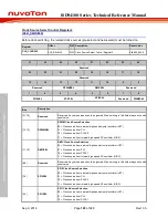
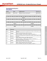
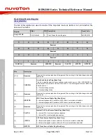
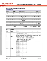
Clock Output Control Register
(CLK_CLKOCTL)
Register
Offset
R/W Description
Reset Value
CLK_CLKOCTL
0x60
R/W Clock Output Control Register
0x0000_0000
31
30
29
28
27
26
25
24
Reserved
23
22
21
20
19
18
17
16
Reserved
15
14
13
12
11
10
9
8
Reserved
7
6
5
4
3
2
1
0
Reserved
CLK1HZEN
DIV1EN
CLKOEN
FREQSEL
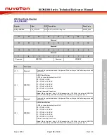
Bits
Description
[31:7]
Reserved
Reserved. Any values read should be ignored. When writing to this field always write with
reset value.
[6]
CLK1HZEN
Clock Output 1Hz Enable Bit
0 = 1 Hz clock output for RTC frequency compensation Disabled.
1 = 1 Hz clock output for RTC frequency compensation Enabled.
Note:
RTC IP need to be enabled.
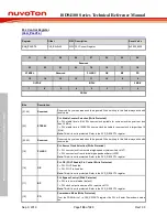
[5]
DIV1EN
Clock Output Divide One Enable Bit
0 = Clock Output will output clock with source frequency divided by FREQSEL.
1 = Clock Output will output clock with source frequency.
[4]
CLKOEN
Clock Output Enable Bit
0 = Clock Output function Disabled.
1 = Clock Output function Enabled.
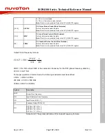
[3:0]
FREQSEL
Clock Output Frequency Selection
The formula of output frequency is
F
out
= F
in
/2
(N+1).
F
in
is the input clock frequency.
F
out
is the frequency of divider output clock.
N is the 4-bit value of FREQSEL[3:0].


