ISD94100 Series Technical Reference Manual
Sep 9, 2019
Page
220
of 928
Rev1.09
IS
D
9
410
0
S
ER
IE
S
T
E
C
HN
ICA
L
RE
F
E
RE
NCE
M
AN
U
AL
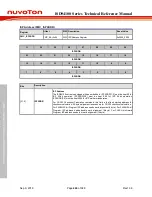
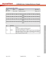
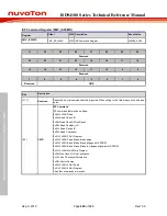
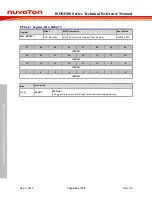
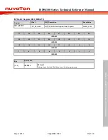
CONFIG1 (Address = 0x0030_0004)
31
30
29
28
27
26
25
24
Reserved
23
22
21
20
19
18
17
16
Reserved
DFBA
15
14
13
12
11
10
9
8
DFBA
7
6
5
4
3
2
1
0
DFBA
Bits
Descriptions
[31:20]
Reserved
Reserved bit should always be programmed with 0.
[19:0]
DFBA
Data Flash Base Address
This register works only when DFEN (CONFIG0[0])set to 0. If DFEN (CONFIG0[0]) is set to
0, the Data Flash base address is defined by user. Since on-chip flash erase unit is 4 Kbytes,
it is mandatory to keep bit 11-0 as 0.
Note:
The bits of configure should be 0 if reserved.

