ISD94100 Series Technical Reference Manual
Sep 9, 2019
Page
243
of 928
Rev1.09
IS
D
9
410
0
S
ER
IE
S
T
E
C
HN
ICA
L
RE
F
E
RE
NCE
M
AN
U
AL
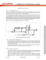
Figure 6.5-3 Open-Drain Output
6.5.5.4
Quasi-bidirectional Mode
Writing 0b11 to MODEn bits (Px_MODE[2n+1:2n]) configures the corresponding Px.n pin as Quasi-
bidirectional mode I/O pin. Under this mode, the I/O pin supports digital output and input function at the
same time however the max source current is only less than 100uA.
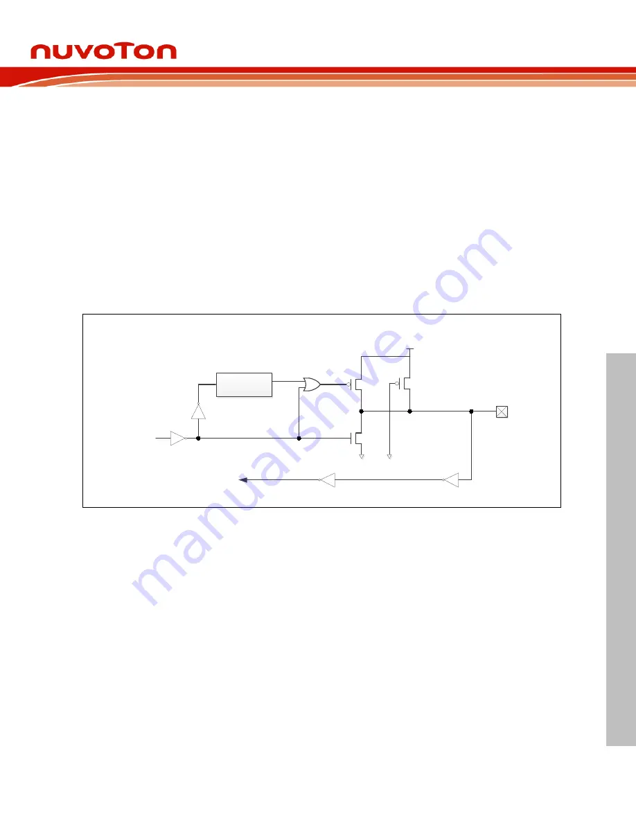
For input operation, before the read operation is performed the DOUT (Px_DOUT[n]) bit must be set to
1. For output operation, if DOUT (Px_DOUT[n]) bit is 0, the pin outputs low to the pin. If DOUT
(Px_DOUT[n]) bit is 1, the device will drives high and also check the pin value. If pin value is high, there
will be no action taken. If pin state is low, then the device will drive strong high for 2 clock cycles and
then disable the strong output drive. Meanwhile, the pin status is controlled by internal pull-up resistor.
Note that the source current capability in quasi-bidirectional mode is only 30~65
μA
.
Figure 6.5-4 shows the Quasi-bidirectional Mode I/O pin architecture.
Port Pin
Port Pin
N
N
P
P
VDD
VDD
Port Latch Data
Port Latch Data
Input Data
Input Data
2 CPU
Clock Delay
P
P
Strong
Strong
Very
Weak
Very
Weak
Figure 6.5-4 Quasi-Bidirectional I/O Mode
6.5.5.5
GPIO Interrupt and Wake-up Function
Each GPIO pin can be configured to generate interrupt by configuring its RHIEN (Px_INTEN[n+16])/
FLIEN (Px_INTEN[n]) bit and TYPE (Px_INTTYPE[n]). There are five types of interrupt condition
can be selected: low level trigger, high level trigger, falling edge trigger, rising edge trigger and both
rising and falling edge trigger.
The GPIO pins can also be the chip wake-up source from Idle/Power-down state. The configuration
of wake-up trigger condition is the same as GPIO interrupt configuration.
6.5.5.6
GPIO De-bounce Function
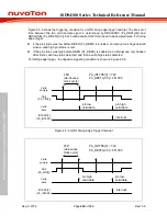
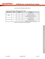
GPIO de-bounce function can be used to sample interrupt input and prevent unexpected interrupt
due to noise. GPIO de-bounce function only applies to edge trigger interrupts, including falling
edge trigger, rising edge trigger and both rising and falling edge trigger.
Writing 1 to Px_DBEN bit enables the de-bounce function for the corresponding pin. The de-
bounce clock source can be from HCLK or LIRC (10kHz) by configuring DBCLKSRC
(Px_DBCTL[4]) register. DBCLKSEL (Px_DBCTL[3:0]) register configures the interrupt sampling
rate.


