ISD94100 Series Technical Reference Manual
Sep 9, 2019
Page
253
of 928
Rev1.09
IS
D
9
410
0
S
ER
IE
S
T
E
C
HN
ICA
L
RE
F
E
RE
NCE
M
AN
U
AL
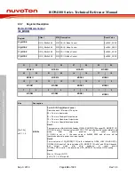
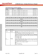
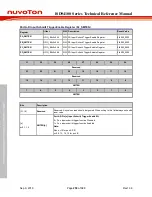
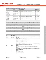
Port A-D De-bounce Enable Control Register (Px_DBEN)
Register
Offset
R/W Description
Reset Value
PA_DBEN
0x014
R/W PA De-Bounce Enable Control Register
0x0000_0000
PB_DBEN
0x054
R/W PB De-Bounce Enable Control Register
0x0000_0000
PC_DBEN
0x094
R/W PC De-Bounce Enable Control Register
0x0000_0000
PD_DBEN
0x0D4
R/W PD De-Bounce Enable Control Register
0x0000_0000
31
30
29
28
27
26
25
24
Reserved
23
22
21
20
19
18
17
16
Reserved
15
14
13
12
11
10
9
8
DBEN
7
6
5
4
3
2
1
0
DBEN
Bits
Description
[31:16]
Reserved
Reserved. Any values read should be ignored. When writing to this field always write with
reset value.
[n]
n=0,1..15
DBEN[n]
Port A-D Pin[n] Input Signal De-bounce Enable Bit
The DBEN[n] bit is used to enable the de-bounce function for each corresponding bit. If
the input signal pulse width cannot be sampled by continuous two de-bounce sample cycle,
the input signal transition is seen as the signal bounce and will not trigger the interrupt.
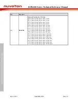
The de-bounce clock source is controlled by DBCLKSRC (GPIO_DBCTL [4]), one de-
bounce sample cycle period is controlled by DBCLKSEL (GPIO_DBCTL [3:0]).
0 = Px.n de-bounce function Disabled.
1 = Px.n de-bounce function Enabled.
The de-bounce function is valid only for edge triggered interrupt. If the interrupt mode is
level triggered, the de-bounce enable bit is ignored.
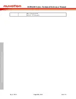
Note:
Max. n=15 for port A/C/D
n=0..9, 13, 14, 15 for port B


